Key Statistics
Key Takeaways
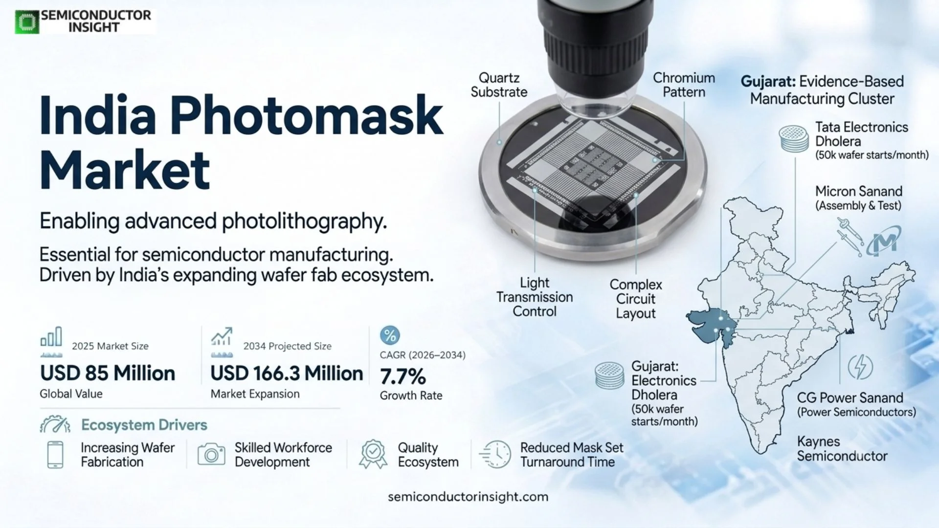
- Gujarat is the strongest manufacturing cluster, combining the Dholera wafer fab with Micron, CG Power and Kaynes semiconductor operations around Sanand.
- Quartz Mask is the strategically important type for semiconductor lithography because dimensional stability, optical quality and defect performance are essential to repeated wafer exposure.
- Semiconductor is the central growth application as India’s first commercial wafer fabs progress from approval and construction toward equipment installation and production.
- Dholera has a planned capacity of 50,000 wafer starts per month and an investment above ₹91,000 crore, creating the largest single direct photomask demand catalyst in the country.
- Uttar Pradesh adds another direct lithography node through the HCL-Foxconn display-driver project with planned capacity of 20,000 wafers per month.
- Local supply remains an opportunity because mask production and repair infrastructure is far less developed than India’s growing fab, packaging and design ecosystem.
India Photomask Market Overview
India Photomask Market was valued at USD 85 million in 2025 and is projected to reach USD 166.3 million by 2034, expanding at a 7.7% CAGR during 2026–2034. Gujarat is the strongest evidence-based manufacturing cluster because it combines the 50,000-wafer-starts-per-month Tata Electronics fab at Dholera with Micron, CG Power and Kaynes semiconductor projects in Sanand. Direct photomask consumption will rise as wafer fabrication comes online, while assembly-and-test investments strengthen the wider supplier, skills and quality ecosystem without consuming masks at the same intensity as wafer fabs.
A photomask is a high-precision quartz, glass or film plate that carries circuit or display patterns used during photolithography. Light projects the patterned image through optical systems onto a photosensitive resist, allowing repeated transfer of device features to semiconductor wafers, display substrates or circuit boards. Mask accuracy, defect control, overlay, critical-dimension uniformity and contamination control directly affect pattern fidelity and manufacturing yield.
India’s market is at an inflection point because domestic semiconductor policy is moving from design and packaging toward wafer fabrication. A conventional assembly-and-test plant creates limited direct photomask demand because lithography has already occurred on the incoming wafer. By contrast, the planned Dholera silicon fab, the Uttar Pradesh display-driver fab and Odisha’s compound-semiconductor project create direct local requirements for masks, mask qualification, inspection, logistics and engineering support as process lines ramp.
The near-term market will remain import-intensive. Leading photomask manufacturing requires e-beam pattern generation, advanced resist processing, defect inspection, cleaning, repair, metrology and tightly controlled blanks. India can still capture value before full domestic mask production develops through local application engineering, secure logistics, inspection support, mask data preparation and strategic inventory near fabs. Those services reduce cycle time and supply risk for customers whose mask sets are both expensive and production-critical.
Segment Analysis: By Type
By type, the market is segmented exactly into Quartz Mask, Soda Mask, Toppan, and Film. The published segmentation contains an unusual “Toppan” label and it is retained as defined rather than renamed. Quartz masks are the most strategically relevant to semiconductor lithography because dimensional stability, flatness and optical performance matter as pattern tolerances tighten.
| Type | Technical / functional role | Market position and purchasing logic |
|---|---|---|
| Quartz Mask | Quartz provides strong optical transmission and dimensional stability for high-precision lithography. Semiconductor mask sets use carefully controlled substrates, opaque absorber patterns and protective handling processes because defects or distortion can print repeatedly across many wafers. | The key value segment for semiconductor fabrication. Demand should expand as domestic wafer fabs ramp, but procurement will remain tied to global qualified mask shops until local pattern generation, inspection and repair infrastructure matures. |
| Soda Mask | Soda-lime glass is used where cost is more important than the thermal and dimensional stability required for advanced semiconductor work. It can support less demanding lithography, display, education and industrial patterning applications. | A cost-sensitive segment suited to larger features and applications that can tolerate less stringent dimensional control. Its role in advanced IC production is limited, but it remains relevant to broader photolithography and pattern-transfer markets. |
| Toppan | This source-defined type label is retained without reinterpretation. Commercially, Toppan Photomasks is also a major global photomask supplier with capabilities spanning semiconductor technology generations and supporting services. | The label should be treated as a source-defined segmentation category in this report. Purchasing decisions in the wider market center on mask technology, defect control, turnaround time and supplier qualification rather than on the label alone. |
| Film | Film photomasks use a patterned photographic layer on flexible substrate and are suitable for lower-resolution or lower-cost imaging where rigid high-precision quartz is unnecessary. | Film serves PCB, educational, prototyping and other coarse-feature applications. It is economical and easy to handle but is not a substitute for precision semiconductor masks where dimensional stability and microscopic defect control are critical. |
Technology and pricing logic
Photomask value rises steeply with feature complexity, defect requirements and inspection burden. A basic film or soda-lime mask competes on cost and turnaround, while semiconductor-grade quartz masks require precision blanks, e-beam writing, clean processing, inspection, metrology and repair. A mask set also represents intellectual property and production risk, so customers evaluate data security, chain of custody and supplier redundancy in addition to nominal price.
Segment Analysis: By Application
By application, the India market is segmented into Semiconductor, Flat Panel Display, Touch Industry, and Circuit Board. Semiconductor is the most important growth engine because approved wafer-fabrication projects create recurring mask demand for device layers, process changes, engineering lots and new product introductions.
| Application | Demand characteristics |
|---|---|
| Semiconductor | Wafer fabs use photomasks repeatedly across lithography steps to define transistors, interconnects and other device structures. Direct domestic demand is set to rise with Dholera, Jewar and compound-semiconductor projects. Each active process flow requires multiple masks, and design revisions or new devices create recurring mask-set orders rather than a one-time purchase. |
| Flat Panel Display | Display fabrication uses large-area masks to pattern thin-film transistor backplanes, electrodes and other structures. India’s current display-fab footprint is limited, so demand is smaller and more project dependent than semiconductor lithography. Future display-manufacturing investment could materially expand the addressable market because panel masks are physically large and technically specialized. |
| Touch Industry | Touch sensors and related patterned conductive structures use photolithography or imaging steps that can require masks depending on process choice. Demand tracks domestic display-module, appliance, automotive and consumer-electronics manufacturing and is generally less technically demanding than advanced semiconductor masks. |
| Circuit Board | PCB fabrication can use phototools or direct imaging to define circuit features. Film masks remain relevant for certain board, prototype and lower-volume processes, while laser direct imaging reduces mask use in advanced PCB plants. This creates a mixed outlook: electronics manufacturing raises PCB output, but imaging technology can reduce physical mask intensity per board. |
Additional segmentation dimensions
| Axis | Source-defined segments | Commercial interpretation |
|---|---|---|
| By Substrate / Format | Quartz; Soda-lime glass; Film-based phototools | Rigid quartz serves precision semiconductor work, glass supports less demanding lithography, and film remains suitable for larger-feature imaging and prototyping. |
| By Service Need | New mask writing; Inspection & metrology; Cleaning & repair; Secure logistics | As domestic fabs develop, service availability becomes as important as blank supply. Faster inspection, repair and secure mask logistics can reduce fab downtime and shorten engineering cycles even before a full local mask-writing ecosystem exists. |
Regional Analysis
Gujarat is the strongest evidence-based photomask demand cluster because the state combines India’s first commercial semiconductor fab project at Dholera with multiple assembly-and-test facilities in Sanand. Uttar Pradesh and Odisha add direct future lithography demand through wafer-fabrication projects, while Assam and Andhra Pradesh are weighted toward packaging and therefore contribute more indirectly through ecosystem development.
Which Indian manufacturing clusters matter most for future photomask demand?
Photomask demand should be assessed by fabrication intensity rather than by semiconductor investment alone. A wafer fab consumes masks directly because lithography is part of front-end manufacturing. ATMP and OSAT plants create strong semiconductor ecosystems but use incoming patterned wafers, so their direct mask demand is limited. The state-level analysis therefore separates direct wafer-fab catalysts from packaging-led clusters to avoid overstating demand.
| Region | Position | Growth outlook | Demand profile | Evidence-led market logic |
|---|---|---|---|---|
| Gujarat | Strongest cluster | Highest direct potential | Wafer fab + ATMP ecosystem | Dholera is planned at 50,000 wafer starts per month; Sanand includes Micron, CG Power and Kaynes projects, concentrating infrastructure, suppliers and skills. |
| Uttar Pradesh | Emerging direct fab cluster | High | Display-driver wafer fab | The HCL-Foxconn joint venture at Jewar is planned for 20,000 wafers per month and 36 million chips per month, creating direct lithography demand. |
| Odisha | Emerging compound-semiconductor cluster | High from small base | SiC fab + advanced packaging | SicSem is approved for 60,000 SiC wafers per year plus 96 million packaged units per year; compound semiconductor lithography creates direct mask requirements. |
| Assam | Packaging ecosystem | Indirect | ATMP-led | TSAT Morigaon is planned at 48 million chips per day. It strengthens semiconductor supply chains and skills but conventional assembly-and-test does not create the same mask intensity as wafer fabrication. |
| Andhra Pradesh | Packaging ecosystem | Indirect / emerging | Advanced package project | ASIP was approved with 96 million units per year capacity. The project expands India’s back-end ecosystem while direct photomask demand remains dependent on future front-end fabrication. |
Competitive Landscape
India remains dependent on global photomask specialists, so competition is shaped by technology capability, turnaround time, defect performance, secure handling and the ability to support new Indian fabs through qualification. The profiled list includes established Japanese, American and Asian suppliers. Local value creation is more likely to begin with logistics, mask data support, inspection partnerships and customer engineering before moving into capital-intensive mask writing and repair.
Toppan Photomasks, Hoya, Dai Nippon Printing and other established suppliers benefit from decades of mask-writing, inspection and semiconductor customer qualification. Their advantage is not simply access to quartz blanks; it is the process control needed to convert design data into defect-controlled masks and to maintain revision, repair and traceability systems across many customer technologies.
Photronics, Taiwan Mask, Compugraphics and specialist suppliers compete across technology nodes and regional customer bases. For India, response time and secure supply will become more important as domestic fabs start engineering lots. A mask written overseas can still be competitive, but transport time, customs, damage risk and repair turnaround create an opening for local service partnerships and buffer strategies.
New domestic entrants face high capital and know-how barriers. E-beam writers, inspection systems, cleanrooms and metrology are expensive, and utilization must be sufficient to justify them. A phased localization route-data preparation, inspection, cleaning, logistics, then selected writing or repair-can reduce risk while building a qualified customer base.
| Competitive tier | Representative companies | How they compete |
|---|---|---|
| Global full-service leaders | Toppan Photomasks, Inc.; Hoya Corporation; Dai Nippon Printing Co., Ltd.; Photronics, Inc. | Compete through advanced writing, inspection, global fab qualification, defect control and the ability to support multiple technology nodes. |
| Regional / specialist mask suppliers | Taiwan Mask Corporation; SK-Electronics Co., Ltd.; Compugraphics; Advance Reproductions | Compete through regional service, selected technology capabilities, turnaround and customer-specific engineering. |
| India localization opportunity | Local logistics, inspection, cleaning, repair and data-service partners | The near-term domestic opportunity is to reduce lead time and supply risk around imported masks while India builds the scale required for capital-intensive mask-writing infrastructure. |
Key Participants
Photomask Supply & Localization Analysis
Photomask production is a precision manufacturing activity rather than a high-volume commodity process. Capacity depends on qualified mask blanks, e-beam writing tools, resist processing, defect inspection, metrology, cleaning, repair and secure data handling. India’s announced wafer-fab pipeline creates a reason to localize parts of this chain, but front-end mask writing will require customer qualification and enough recurring mask volume to support expensive equipment and specialist workforce.
Near-term supply will rely heavily on imported masks from established global facilities. This can serve early fab ramps, but cycle time becomes important when engineering lots need rapid mask revisions. Secure air freight, customs procedures, local storage and incoming inspection are therefore commercially important parts of the supply chain rather than administrative details.
Localization can proceed in stages. India can first build mask data preparation, cleaning, inspection coordination, repair partnerships and logistics around Gujarat and other fab clusters. As mask volumes and technology mix become clearer, suppliers can evaluate domestic pattern generation or joint ventures without assuming that all advanced equipment must be installed from day one.
The strongest demand signal comes from front-end wafer projects. Dholera at 50,000 wafer starts per month, Jewar at 20,000 wafers per month and Odisha’s 60,000 SiC wafers per year create visible future lithography requirements. Packaging plants are important ecosystem investments but should not be counted as equivalent mask capacity drivers because their wafers arrive after front-end patterning.
Market Dynamics
India’s photomask market is being reshaped by the transition from a design- and assembly-heavy semiconductor ecosystem toward domestic front-end fabrication. The addressable market grows as fabs require mask sets for technology qualification, new products and revisions. At the same time, reliance on imported masks, stringent defect requirements, intellectual-property sensitivity and uncertain initial fab utilization limit the pace at which local mask manufacturing can scale.
Market Drivers
Growth drivers and directional market impact
| Driver | Directional impact* | Why it matters |
|---|---|---|
| Domestic wafer fabrication investment | High | The Dholera, Jewar and Odisha fab projects create direct lithography demand. Dholera alone is planned for 50,000 wafer starts per month, while Jewar adds 20,000 wafers per month. Mask demand rises with process layers, product introductions and engineering revisions as these fabs move into qualification and production. |
| Government semiconductor incentives | High | India’s semiconductor program provides fiscal support for fabrication and packaging projects, reducing the capital barrier for domestic manufacturing. The policy effect on photomasks is indirect but material: every front-end fab that reaches production creates recurring demand for qualified masks and related services. |
| Automotive, power and electronics demand | Medium-High | EVs, power electronics, telecom, consumer electronics and industrial systems create local chip demand. The Odisha SiC fab specifically targets EV, rail, chargers, data centers, appliances, defense and solar applications, linking end-market growth to domestic lithography requirements. |
| Need for shorter engineering cycles | Medium | Fab engineers need rapid mask revisions during process development and product ramp. Long international logistics can extend cycle time, creating a commercial case for local inspection, repair coordination, mask data services and eventually domestic writing capability. |
Domestic wafer fabrication investment
The Dholera, Jewar and Odisha fab projects create direct lithography demand. Dholera alone is planned for 50,000 wafer starts per month, while Jewar adds 20,000 wafers per month. Mask demand rises with process layers, product introductions and engineering revisions as these fabs move into qualification and production.
Government semiconductor incentives
India’s semiconductor program provides fiscal support for fabrication and packaging projects, reducing the capital barrier for domestic manufacturing. The policy effect on photomasks is indirect but material: every front-end fab that reaches production creates recurring demand for qualified masks and related services.
Automotive, power and electronics demand
EVs, power electronics, telecom, consumer electronics and industrial systems create local chip demand. The Odisha SiC fab specifically targets EV, rail, chargers, data centers, appliances, defense and solar applications, linking end-market growth to domestic lithography requirements.
Need for shorter engineering cycles
Fab engineers need rapid mask revisions during process development and product ramp. Long international logistics can extend cycle time, creating a commercial case for local inspection, repair coordination, mask data services and eventually domestic writing capability.
Market Restraints
Constraints and directional market impact
| Restraint | Directional impact* | Commercial effect |
|---|---|---|
| High capital intensity of mask manufacturing | High | Advanced photomask facilities require e-beam writers, inspection, metrology and ultra-clean process infrastructure. Early Indian demand may be insufficient to keep a full technology range efficiently utilized, favoring phased localization and partnerships with established global suppliers. |
| Dependence on imported precision equipment and blanks | Medium-High | Mask blanks, writing tools and inspection systems are specialized global products. Long lead times, export controls or supplier concentration can affect localization schedules and reinforce the importance of qualified dual-source strategies. |
| Intellectual-property and data-security requirements | Medium | A photomask contains the physical representation of proprietary circuit layouts. Customers require secure data transfer, access controls and chain-of-custody procedures, which raises the operational standard for new service providers and can limit casual outsourcing. |
| Fab ramp timing and utilization risk | Medium-High | Photomask demand follows actual wafer process qualification and production, not announced investment alone. Construction delays, slower equipment ramp or lower initial utilization can postpone mask orders, making capacity planning difficult for a new domestic supplier. |
High capital intensity of mask manufacturing
Advanced photomask facilities require e-beam writers, inspection, metrology and ultra-clean process infrastructure. Early Indian demand may be insufficient to keep a full technology range efficiently utilized, favoring phased localization and partnerships with established global suppliers.
Dependence on imported precision equipment and blanks
Mask blanks, writing tools and inspection systems are specialized global products. Long lead times, export controls or supplier concentration can affect localization schedules and reinforce the importance of qualified dual-source strategies.
Intellectual-property and data-security requirements
A photomask contains the physical representation of proprietary circuit layouts. Customers require secure data transfer, access controls and chain-of-custody procedures, which raises the operational standard for new service providers and can limit casual outsourcing.
Fab ramp timing and utilization risk
Photomask demand follows actual wafer process qualification and production, not announced investment alone. Construction delays, slower equipment ramp or lower initial utilization can postpone mask orders, making capacity planning difficult for a new domestic supplier.
Market Opportunities
Local mask inspection and repair services
Inspection, cleaning and repair can reduce turnaround time without requiring a complete advanced mask-writing operation. Gujarat is the strongest initial location because Dholera and Sanand concentrate semiconductor activity and logistics demand.
Partnerships with global photomask leaders
Joint ventures or service alliances can combine proven process technology with Indian customer access and incentives. A partner-led model can reduce qualification risk and provide local support while high-end pattern generation remains connected to an existing global mask network.
Mature-node and compound-semiconductor masks
India’s first fabs emphasize mature silicon, display-driver and SiC technologies rather than the most advanced logic nodes. This creates an opportunity to localize selected mask technologies with lower capital and inspection complexity before moving toward more demanding nodes.
Secure digital-to-mask workflow
Design-data preparation, encryption, version control and automated handoff from Indian design teams to mask shops can reduce errors and protect IP. Software and engineering services can therefore capture value even when physical mask production is offshore.
Supply Chain Analysis
1. Mask blanks & materials
2. Pattern generation
3. Inspection, metrology & repair
4. Fab logistics & lifecycle
Mask blanks & materials
High-quality blanks must meet flatness, defect and optical requirements before pattern generation. India will initially depend on global suppliers, so incoming quality, secure storage and lead-time planning matter.
Pattern generation
Design data is fractured and written onto the mask with precision pattern-generation tools. This is a high-capital step requiring process recipes, calibration and tight data-security controls.
Inspection, metrology & repair
Masks must be inspected for defects and dimensional accuracy before fab use. Local service capability can shorten revision and recovery cycles and is a realistic early localization opportunity.
Fab logistics & lifecycle
Masks move between supplier and fab under strict contamination, damage and IP controls. Lifecycle management includes new versions, repairs, retirement and emergency replacement, making logistics a recurring service requirement.
Recent Developments
Micron opened its Sanand assembly-and-test facility
Micron announced commercial production at its Sanand site and said it expects to assemble and test tens of millions of chips in 2026, scaling to hundreds of millions in 2027. The site is a back-end operation, so its photomask impact is indirect, but it materially strengthens Gujarat’s semiconductor workforce and supply ecosystem. Micron
India approved four additional semiconductor projects
Government approval included SicSem and 3D Glass Solutions in Odisha, CDIL in Punjab and ASIP in Andhra Pradesh. SicSem’s 60,000-wafer-per-year SiC fab is directly relevant to photomasks because front-end device fabrication requires lithography. Press Information Bureau
HCL-Foxconn display-driver fab added a new direct lithography node
Government project disclosures list the Uttar Pradesh joint venture at ₹3,706 crore with planned capacity of 20,000 wafers per month and 36 million chips per month. The project broadens India’s future front-end mask demand beyond Gujarat. Press Information Bureau
Fiscal support agreement signed for the Dholera fab
India Semiconductor Mission and Tata entities signed the fiscal support agreement for the Dholera fab. The project is planned for 50,000 wafer starts per month with investment above ₹91,000 crore, making it the largest visible future direct photomask demand catalyst in India. Press Information Bureau
Report Scope & Segmentation
| Attribute | Scope |
|---|---|
| Market | India Photomask |
| Base Year | 2025 |
| Estimated Year | 2026 |
| Forecast Period | 2026–2034 |
| 2025 Market Size | USD 85 million |
| 2034 Market Size | USD 166.3 million |
| CAGR | 7.7% (2026–2034) |
| Largest Market | Gujarat semiconductor cluster |
| By Type | Quartz Mask; Soda Mask; Toppan; Film |
| By Application | Semiconductor; Flat Panel Display; Touch Industry; Circuit Board |
| Key Indian Demand Clusters | Gujarat; Uttar Pradesh; Odisha; Assam; Andhra Pradesh |
| Regions | India – state-level manufacturing clusters |
| Key Companies | Toppan Photomasks, Inc., Hoya Corporation, Nippon Filcon Co., Ltd., Photronics, Inc., SK-Electronics Co., Ltd., Compugraphics, Taiwan Mask Corporation, Dai Nippon Printing Co., Ltd., Shin-Etsu MicroSi, Advance Reproductions |
Frequently Asked Questions
What is the India Photomask market size in 2025?
The India Photomask market is valued at USD 85.0 million in 2025. The consistent series uses the report’s published USD 78.9 million value for 2024 and USD 123.4 million endpoint for 2030. Demand currently spans semiconductor, display, touch and circuit-board applications, with the strongest future growth expected from domestic wafer fabrication as approved projects move into production.
What will the India Photomask market reach by 2034?
The market is projected to reach USD 166.3 million by 2034, with an estimated USD 91.6 million in 2026 and a 7.7% CAGR during 2026–2034. The growth outlook depends on actual fab commissioning and utilization, because front-end wafer fabrication generates far more direct mask demand than assembly-and-test projects.
Which Indian state is the strongest photomask demand cluster?
Gujarat is the strongest evidence-based cluster because the state combines the Tata Electronics Dholera fab at 50,000 wafer starts per month with Micron, CG Power and Kaynes semiconductor projects in Sanand. Dholera creates direct lithography demand, while the back-end projects strengthen supplier networks, cleanroom skills and semiconductor logistics around the same state.
Which photomask type is most important for semiconductors?
Quartz masks are the strategically important type for semiconductor lithography because quartz provides dimensional stability and optical performance suitable for repeated precision pattern transfer. Semiconductor masks also require stringent defect inspection, critical-dimension control, cleaning and repair. Film and soda-lime masks remain relevant to less demanding imaging applications where cost is more important than advanced lithography performance.
Which application will drive growth fastest?
Semiconductor fabrication is the central growth application because India is adding front-end wafer projects rather than relying only on chip design and packaging. Dholera, Jewar and Odisha create direct recurring mask requirements for process layers, technology qualification, engineering changes and new device programs. Flat-panel, touch and PCB uses remain part of the market but have different technology and volume profiles.
How much direct photomask demand comes from ATMP or OSAT plants?
Conventional ATMP and OSAT plants create much less direct photomask demand than wafer fabs because the transistors and interconnect patterns are already formed on incoming wafers. Packaging can use patterned substrates and advanced processes, but it should not be treated as equivalent to front-end lithography. Its main photomask benefit is indirect through ecosystem scale, skills, suppliers and future local chip programs.
Why is Dholera important to the market?
The Dholera fab is planned for 50,000 wafer starts per month and investment above ₹91,000 crore. That scale creates recurring requirements for multiple mask layers across qualified processes and products. As engineering lots, new devices and process revisions are introduced, mask demand can recur even without a proportional increase in wafer volume, making the fab a structural demand anchor.
What are the main market restraints?
The main restraints are high capital intensity for mask writing and inspection, dependence on imported precision equipment and blanks, IP and data-security requirements, and uncertainty around the timing and utilization of new fabs. These factors favor a phased localization model in which logistics, inspection, repair and data services develop before a full range of domestic mask-writing capability.
Who are the key companies in the India Photomask market?
The profiled companies are Toppan Photomasks, Hoya Corporation, Nippon Filcon, Photronics, SK-Electronics, Compugraphics, Taiwan Mask Corporation, Dai Nippon Printing, Shin-Etsu MicroSi and Advance Reproductions. Competition centers on patterning capability, defect control, turnaround, fab qualification, secure handling and global capacity rather than simply on substrate price.
Where are the strongest opportunities through 2034?
The strongest opportunities are local inspection and repair, secure mask logistics, design-data services, partnerships with global suppliers and selected localization for mature-node or compound-semiconductor masks. Gujarat offers the clearest early service hub, while Uttar Pradesh and Odisha create additional direct fab nodes. Suppliers should scale with actual fab qualification and utilization rather than announced investment alone.
Research Sources & Evidence Base
View research sources used for this overview
- Press Information Bureau, Government of India. Fiscal Support Agreement for Semiconductor Fab in Dholera, Dholera investment and 50,000-wafer-starts-per-month capacity, 5 March 2025.
- Press Information Bureau, Government of India. Mapping India’s Semiconductor Ecosystem, state-level project capacities for Gujarat, Uttar Pradesh, Odisha, Assam and Andhra Pradesh.
- Press Information Bureau, Government of India. Four additional semiconductor projects approved, SicSem SiC fab and other August 2025 semiconductor approvals.
- Micron Technology. Micron Celebrates Opening of India’s First Semiconductor Assembly and Test Facility, Sanand facility opening, production ramp and cleanroom evidence, 28 February 2026.
Get Sample Report PDF for Exclusive Insights
Report Sample Includes
- Table of Contents
- List of Tables & Figures
- Charts, Research Methodology, and more...
 Download Sample Report PDF