Key Statistics
Key Takeaways
- ArF immersion systems are the highest-performance DUV segment, supporting advanced logic and memory layers where high numerical aperture, overlay control and high throughput justify premium system cost.
- Artificial Intelligence is an important downstream demand application because AI compute increases semiconductor demand, while healthcare and consumer electronics create additional requirements for logic, analog, sensor and display-related chips.
- India is the complete geographic market. Within the country, Gujarat is the most important direct front-end opportunity because the Tata-PSMC Dholera fab is planned at 50,000 wafer starts per month.
- DUV remains essential even in an EUV era. ASML states that many layers in advanced chips continue to be printed with dry and immersion DUV systems, and the company sold 279 DUV lithography systems in 2025.
- India’s fab pipeline is the main demand trigger. Government reporting identified 10 approved semiconductor projects by early 2026, including two fabs and eight packaging units, creating a broader ecosystem for equipment, service, training and materials.
India DUV Lithography Systems Market Overview
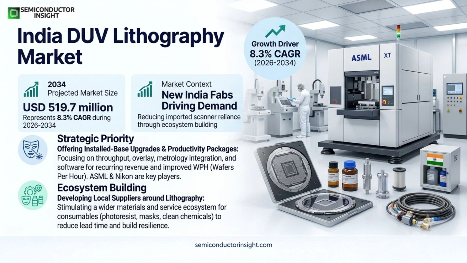
India DUV Lithography Systems market is valued at USD 253.9 million in 2025 and is projected to reach USD 519.7 million by 2034, representing an 8.3% CAGR during 2026–2034. The 2026 estimated market size is USD 275.0 million. India is the sole geographic market, with demand increasingly tied to front-end semiconductor fabs and the supporting ecosystem being built under national semiconductor manufacturing programs.
Deep-ultraviolet lithography uses excimer-laser light to project circuit patterns from a reticle onto photoresist-coated wafers. The market covers ArF dry, ArF immersion and KrF systems. ASML describes immersion DUV as a high-volume manufacturing workhorse, while dry DUV remains cost-effective for many non-critical layers. New Indian fabs therefore need a mix of lithography tools matched to node, wafer size, layer resolution and product architecture rather than one exposure technology for every layer.
India’s strongest direct demand signal is the Tata Electronics fab in Dholera, Gujarat. The Government of India states that the project will have 50,000 wafer starts per month and a technology partnership with PSMC. The announced product scope includes 28 nm high-performance compute and power-management chips. A fab at that scale requires repeated lithography capacity across process layers, together with track systems, metrology, masks, resist, service and trained process engineers.
The broader ecosystem is expanding beyond one project. Government updates in 2026 reported 10 approved semiconductor projects, including two fabs and eight packaging units. Packaging plants do not consume front-end DUV steppers in the same way as wafer fabs, so they should not be counted as equivalent lithography demand. They still matter because they build talent, logistics, materials and customer ecosystems that can support future front-end investment.
Segment Analysis: By Type
By type, the market is segmented into ArF Dry Excimer Systems, ArF Immersion Excimer Systems and KrF Excimer Systems. ArF immersion provides the highest DUV resolution and is critical for more advanced layers, while dry ArF and KrF remain economically important for less demanding layers and mature process nodes.
| Type | Technical role | Market position |
|---|---|---|
| ArF Dry Excimer Systems | ArF dry uses 193 nm light without the water immersion layer. It can print finer features than KrF and is used for selected logic, memory, sensor and other layers where its resolution and overlay performance are adequate. The technology can provide a lower-cost exposure option than immersion when the process layer does not need the additional numerical aperture. | A strategic middle tier. Nikon’s NSR-S333F announced in September 2025 targets logic, memory and image sensors with resolution at or below 65 nm and throughput above 300 wafers per hour, demonstrating continued investment in dry ArF productivity and overlay rather than treating the platform as a frozen legacy technology. |
| ArF Immersion Excimer Systems | ArF immersion uses water between the final lens and wafer to increase numerical aperture. ASML’s immersion platforms use NA 1.35 and serve demanding high-volume logic and memory layers. The technology requires advanced fluid handling, wafer-stage precision, overlay control and process matching with coating, development and metrology systems. | Highest-performance DUV segment. It carries the highest technical and service requirements and is most relevant where Indian fabs pursue finer process layers, multi-patterning or products that need tight overlay and imaging control. Its economics depend on using immersion only where the process layer needs the added resolution and productivity. |
| KrF Excimer Systems | KrF uses 248 nm light and is widely applied to mature-node and less critical process layers. The lower acquisition and operating cost can make KrF attractive for analog, power, display-related and established logic processes where its resolution is sufficient, allowing fabs to reserve more expensive ArF tools for tighter layers. | A durable mature-node segment. India plans substantial production in 28 nm and power-management technologies, so KrF and other mature DUV tools can remain economically important even as selected layers require ArF capability. Scanner matching, uptime and service support can matter as much as maximum resolution in these cost-sensitive layers. |
Lithography platform role inside a fab
A wafer fab uses several lithography classes across different layers rather than choosing one scanner technology for the whole device. ASML notes that even chips using EUV can still print many layers with older DUV technology because it is less expensive where resolution allows. India’s DUV opportunity is therefore linked to the total mask-layer mix, tool productivity, redundancy and process qualification of each fab rather than a simple DUV-versus-EUV substitution decision.
| Platform | Typical use | Commercial implication |
|---|---|---|
| ArF immersion | Used on more demanding front-end layers requiring high resolution, tight overlay and high-volume manufacturing stability. Immersion increases numerical aperture and therefore imaging capability compared with dry ArF, but adds greater tool and process complexity. | High system value, complex service and strong dependence on installed-base support, process control and uptime. Fabs justify immersion where its resolution or patterning economics improve the total cost of producing a qualified wafer. |
| ArF dry | Used on intermediate-resolution layers across logic, memory, sensors and related products. Dry ArF avoids immersion-fluid complexity while retaining 193 nm exposure, making it attractive where KrF is insufficient but immersion is not economically necessary. | Continued innovation in throughput and overlay can keep dry ArF attractive for many production layers. Nikon’s new platform demonstrates that manufacturers still see a large installed and future market for productivity improvements in this class. |
| KrF | Used on mature-node and less critical layers where 248 nm imaging provides adequate resolution. KrF scanners have a large global installed base and can offer lower cost per exposure for layers that do not need 193 nm imaging. | Large addressable role in mixed-node fabs because cost per wafer can be lower than using a more advanced scanner unnecessarily. Mature-node production and power or analog devices can sustain demand for new systems, upgrades and long-term service. |
Segment Analysis: By Application
By application, the market covers Artificial Intelligence, Healthcare, Consumer Electronics and Others. These are downstream chip-demand categories rather than lithography process categories. Their relevance is that higher semiconductor consumption and local manufacturing create the business case for Indian wafer fabs that, in turn, procure DUV exposure systems.
| Application | Demand characteristics |
|---|---|
| Artificial Intelligence | AI infrastructure increases demand for compute, networking, memory, power management and supporting analog devices. India may not initially manufacture the most advanced AI accelerators domestically, but AI-related systems still expand demand for mature-node companion chips and create a stronger economic case for local semiconductor capacity, fab utilization and process equipment investment. |
| Healthcare | Medical imaging, diagnostics, monitoring and connected devices use sensors, analog ICs, microcontrollers and power-management chips. These products often value long lifecycle and reliability over the smallest process node, which aligns with DUV-based mature-node manufacturing and can support domestic fabs serving healthcare electronics supply chains. |
| Consumer Electronics | Phones, PCs, appliances and display systems use a broad mix of logic, analog, power and display-driver chips. India’s large electronics manufacturing base creates demand for local semiconductor supply, and the HCL-Foxconn project in Uttar Pradesh is intended to manufacture display-driver chips for mobile phones, laptops, automobiles and PCs. |
| Others | Automotive, telecom, defense, industrial and power-electronics devices create diverse mature-node requirements. The Tata Dholera fab’s announced markets include automotive, communications, computing and artificial intelligence, while national semiconductor policy aims to build a more complete design-to-manufacturing ecosystem that can support additional wafer-fab investment. |
Regional Analysis
India is a single-country market, so regional analysis is best understood through manufacturing clusters rather than global regions. Gujarat has the largest direct front-end lithography opportunity through the Tata Dholera fab and associated Sanand semiconductor projects. Uttar Pradesh and Odisha add front-end or specialized wafer projects, while Assam and other states strengthen packaging and ecosystem capabilities that support future fab investment.
Which Indian manufacturing clusters matter most for DUV lithography demand?
Only wafer-fabrication projects create direct front-end DUV exposure demand. Packaging and ATMP facilities are therefore treated as ecosystem support rather than as equivalent lithography customers. Official project data show the strongest direct opportunities in Gujarat, Uttar Pradesh and selected specialized wafer projects, while Assam, Punjab and Andhra Pradesh contribute packaging, component and talent infrastructure that can improve the economics of future semiconductor manufacturing.
| Region | Market position | Growth outlook | Demand profile | What decides supplier selection |
|---|---|---|---|---|
| Gujarat | Largest direct opportunity | High | Front-end fab and packaging cluster | Fab schedule, tool qualification, utilities and service |
| Uttar Pradesh | Emerging front-end opportunity | High | Display-driver wafer manufacturing | Process technology, customer ramp and equipment sourcing |
| Odisha | Specialized wafer opportunity | Moderate to high | Compound semiconductor and integration | Tool set, wafer volume and process qualification |
| Assam | Packaging ecosystem | Moderate indirect | Advanced assembly and test | Talent, logistics and supply-chain depth |
| Other India | Supporting ecosystem | Moderate indirect | Packaging, design and components | Skills, infrastructure and future fab pipeline |
Competitive Landscape
The market includes ASML, Nikon, Canon, Carl Zeiss, SUSS MicroTec, EV Group, Veeco Instruments, Ushio, JEOL and Heidelberg Instruments Mikrotechnik, but these companies do not all compete directly in the same DUV scanner category. ASML and Nikon are direct front-end DUV scanner suppliers, Canon participates in semiconductor lithography and related exposure platforms, while several others provide optics, mask aligners, light sources, metrology or adjacent process equipment.
ASML is the dominant global supplier of advanced optical lithography and continues to invest in DUV. Its 2025 annual report records 279 DUV lithography-system sales versus 48 EUV systems, demonstrating that DUV remains a large commercial platform even as EUV expands. The company’s product portfolio spans ArF immersion, ArF dry, KrF and i-line systems, allowing customers to match exposure technology to process-layer economics.
Nikon remains an important competitive alternative in ArF and KrF. In September 2025 it announced the NSR-S333F dry ArF scanner with throughput above 300 wafers per hour and initial deliveries planned for the second half of 2026. Nikon’s lineup also includes ArF immersion scanners. For Indian customers, a second qualified supplier can matter for procurement leverage, installed-base strategy and long-term service competition.
The broader company list should be interpreted carefully. Carl Zeiss is a critical optical-technology supplier, while SUSS MicroTec and EV Group are stronger in mask aligners, bonding and specialty lithography, and Ushio supplies light-source technologies. Their presence is relevant to the wider lithography ecosystem, but it would be misleading to rank all of them as direct competitors for advanced front-end DUV scanner purchases.
Competitive tier structure
| Tier | Companies | Basis of competition |
|---|---|---|
| Direct front-end DUV leaders | ASML; Nikon; Canon | Scanner platforms, imaging, overlay, throughput, installed-base service and process support. These suppliers compete most directly for front-end exposure capital where fabs need high-volume wafer scanners and long-term application engineering. |
| Lithography / process specialists | SUSS MicroTec; EV Group; Heidelberg Instruments | Mask aligners, specialty exposure, advanced-packaging and research lithography rather than direct substitution for every front-end scanner. Their equipment can be important in compound semiconductors, MEMS, research and packaging flows. |
| Adjacent technology suppliers | Carl Zeiss; Veeco Instruments; Ushio; JEOL | Optics, light sources, process and metrology technologies that support the broader lithography and semiconductor-equipment ecosystem. These companies influence performance and process capability but should not be treated as identical scanner competitors. |
Key companies profiled in the report scope
- ASML
- Nikon
- Canon
- Carl Zeiss
- SUSS MicroTec
- EV Group
- Veeco Instruments
- Ushio
- JEOL
- Heidelberg Instruments Mikrotechnik
India DUV Lithography Deployment Capacity Analysis
India’s DUV capacity will be created project by project as front-end fabs move from construction to tool installation and qualification. The key metric is wafer-start capacity at fabs that actually require front-end patterning. Packaging plants should be treated separately because their exposure tools and process requirements differ from the DUV scanners used in silicon wafer fabrication.
The Tata Dholera project is the largest clearly documented front-end capacity driver at 50,000 wafer starts per month. A fab of that scale needs multiple exposure tools to meet cycle-time and uptime requirements, but the exact number and mix of ArF immersion, ArF dry and KrF scanners depend on the process flow, layer count, redundancy philosophy and production mix. No defensible public tool count should be inferred solely from wafer-start capacity.
Supplier support capacity is almost as important as the number of scanners. Lithography systems require installation, calibration, optics and stage maintenance, software upgrades, spare parts and application engineering. As India’s installed base grows, global vendors may need more local field-service engineers and parts inventory. The pace of that localization will depend on when fabs reach tool-install and production-ramp milestones.
Market Dynamics
The market is driven by India’s transition from semiconductor design and electronics assembly toward front-end wafer manufacturing. Government incentives, fab construction and demand from AI, consumer, automotive and communications applications support growth. The main restraints are extreme capital intensity, skills, infrastructure, global equipment dependence and the risk that project schedules move more slowly than policy announcements.
MARKET DRIVERS
Drivers Impact Analysis*
| Factor | Forecast impact* | Geographic relevance | Impact timeline |
|---|---|---|---|
| Execution of the Tata Dholera fab | High | Gujarat | Short to medium term |
| National semiconductor policy support | High | India | Medium to long term |
| Consumer, automotive and AI chip demand | Medium to high | India | Medium term |
| Growth of local semiconductor ecosystem | Medium | Multiple states | Long term |
*Directional analytical rating used to compare market forces; it is not a measured contribution to the headline CAGR.
Dholera creates the first large direct DUV demand pool
The Tata-PSMC fab is planned at 50,000 wafer starts per month and targets 28 nm high-performance compute and power-management products. That creates a clear requirement for production lithography across many process layers. The size and technology mix make the project the most important single demand driver for India’s DUV equipment market through the current build cycle.
Policy support reduces the cost of building semiconductor capacity
India’s semiconductor programs provide fiscal support for fabs and packaging facilities, and the second policy phase extends long-term backing. Equipment purchases are a major portion of fab capital cost, so government support improves project economics and increases the probability that approved projects reach tool-order and installation stages rather than remaining announcements.
Electronics manufacturing creates a domestic demand argument
India already produces large volumes of phones, computers, automotive electronics and other devices. The HCL-Foxconn project is intended to make display-driver chips for mobile phones, laptops, automobiles and PCs. A larger local electronics base gives fabs potential domestic customers and strengthens the business case for investing in front-end manufacturing equipment.
A broader ecosystem lowers future execution risk
Packaging, design incentives, components and semiconductor training do not directly create DUV scanner demand, but they help build engineers, suppliers, logistics and quality systems. As this ecosystem matures, new fab projects face lower support risk. Equipment vendors can justify local field-service and application teams once there is enough installed semiconductor capacity to keep those resources productive.
MARKET RESTRAINTS
Restraints Impact Analysis*
| Factor | Forecast impact* | Geographic relevance | Impact timeline |
|---|---|---|---|
| Very high capital cost | High | All front-end fab projects | Persistent |
| Limited local lithography service skills | High | India | Short to medium term |
| Dependence on global equipment suppliers | High | India | Persistent |
| Project schedule and ramp risk | High | New fab clusters | Medium term |
*Directional analytical rating used to compare market forces; it is not a measured contribution to the headline CAGR.
Lithography is one of the most capital-intensive fab tool categories
Advanced DUV systems combine precision optics, high-power lasers, wafer stages, vibration control and complex software. The purchase price is only part of lifecycle cost; fabs also need installation, cleanroom infrastructure, service contracts, spare parts and process engineering. New Indian fabs must absorb these costs before production yield and utilization are established.
Local operating experience is still developing
DUV scanners require specialized process, maintenance and application engineers. India has strong semiconductor design talent but a smaller base of high-volume front-end fab experience. Vendors and fab operators need training programs, international knowledge transfer and field-service localization. A shortage of experienced personnel can slow installation, qualification and yield ramp even when equipment arrives on schedule.
Equipment sourcing is globally concentrated
Front-end DUV scanners are supplied by a very small number of global vendors, so Indian projects cannot easily substitute local equipment if delivery, service or supply-chain issues arise. This makes procurement timing and long-term vendor relationships important project risks. The same concentration raises the value of securing service capability, spare parts and application support early.
Approved projects can still face execution delays
Fab construction, utilities, cleanroom qualification, process licensing and customer qualification all have to align before lithography systems generate productive wafer starts. Market demand should therefore follow actual construction and tool-install milestones rather than policy approvals alone. A schedule slip at one large fab can materially change annual equipment demand in a relatively small national market.
MARKET OPPORTUNITIES
Build local lithography service and training capability
Global equipment suppliers can create a durable Indian position by developing local field-service engineers, application support and spare-parts logistics before the installed base becomes large. Customers gain faster response and lower downtime risk, while vendors create service revenue and closer relationships that can influence future tool purchases, upgrades and process expansions.
Target mature-node and mixed-technology fabs
India’s announced front-end projects include 28 nm and power-management products that do not rely solely on the most advanced lithography. ArF dry, ArF immersion and KrF systems can all have roles across different layers. Suppliers that optimize cost per wafer rather than pushing only the most advanced scanner can align better with India’s initial fab economics.
Offer installed-base upgrades and productivity packages
ASML emphasizes upgradeability across DUV platforms, and Nikon continues to improve throughput and overlay. Once scanners are installed, productivity improvements, overlay control, metrology integration and software upgrades can become a recurring revenue stream. For a new fab, improving wafers per hour can defer additional capital spending while raising output from the same cleanroom footprint.
Develop local suppliers around lithography operations
Lithography requires photoresist, masks, pellicles, clean chemicals, filtration, precision temperature control and metrology. India’s equipment market can therefore stimulate a wider materials and service ecosystem. Localizing selected consumables and non-core support functions can reduce lead time and build resilience even though the scanner itself remains imported.
India DUV Lithography Supply Chain Analysis
Critical subsystems remain globally specialized
DUV scanners depend on excimer lasers, ultra-high-quality optics, precision mechatronics, vibration control and advanced software. These are not commodity inputs. The technical concentration creates high entry barriers and means India’s early market will rely heavily on imported systems and service knowledge rather than a rapidly localized scanner supply chain.
System OEMs integrate performance and lifecycle support
The scanner manufacturer is responsible not only for exposure resolution but also overlay, throughput, matching, diagnostics and upgrades. ASML’s 2025 sales of 279 DUV systems show the global installed-base scale behind its service model. Nikon’s new NSR-S333F shows that dry ArF continues to receive new platform investment rather than being a frozen legacy technology.
Fab installation converts capital equipment into productive capacity
A delivered scanner does not create revenue until utilities, tracks, masks, process recipes and metrology are qualified together. Indian fabs need vendor application engineers and process teams to stabilize yield and overlay. Early ramp performance will influence whether later tool purchases favor the same supplier, making first installations commercially important.
End-market demand sets utilization and future tool orders
A fab can justify additional scanners when customer demand raises utilization and process bottlenecks appear. India’s electronics, automotive and AI-related markets therefore matter indirectly through wafer demand. If local fabs win stable product programs, equipment orders can progress from initial line build to capacity expansion and installed-base upgrades.
Recent Developments in the India DUV Lithography Systems Market
India approves the second phase of its semiconductor program
The Government of India approved a long-term second phase of semiconductor policy support with a ₹1,27,500 crore outlay. The program is intended to deepen design and manufacturing capability and can improve confidence for equipment and service suppliers evaluating long-term investment in India.
Nikon launches the NSR-S333F dry ArF scanner
Nikon announced a new ArF scanner with resolution at or below 65 nm, overlay of 4 nm or better and throughput above 300 wafers per hour. Initial deliveries are planned for the second half of 2026, showing continued innovation in DUV platforms relevant to mature and mixed-node fabs.
India approves four additional semiconductor projects
The Cabinet approved four projects in Odisha, Punjab and Andhra Pradesh with combined investment near ₹4,600 crore. The projects broaden India’s semiconductor manufacturing ecosystem, though only wafer-fabrication projects create direct front-end DUV scanner demand.
Fiscal support agreement signed for Tata’s Dholera fab
India Semiconductor Mission and Tata signed the fiscal-support agreement for the Dholera project, reiterating investment above ₹91,000 crore and planned capacity of 50,000 wafer starts per month. This remains the largest direct front-end lithography opportunity in the country.
REPORT SCOPE & SEGMENTATION
| Attribute | Details |
|---|---|
| Study Period | 2019–2034 |
| Base Year | 2025 |
| Estimated Year | 2026 |
| Forecast Period | 2026–2034 |
| Historical Period | 2019–2025 |
| Market Size 2025 | USD 253.9 million |
| Market Size 2034 | USD 519.7 million |
| Growth Rate | CAGR of 8.3% from 2026–2034 |
| Unit | Value (USD Million) and installed systems where applicable |
| Segmentation | By Type, By Application, India Market |
| By Type | ArF Dry Excimer Systems · ArF Immersion Excimer Systems · KrF Excimer Systems |
| By Application | Artificial Intelligence · Healthcare · Consumer Electronics · Others |
| By Region | India-only market analysed through major semiconductor manufacturing clustersIndiaGujarat, Uttar Pradesh, Odisha, Assam and other semiconductor ecosystem locations |
| Key Companies Profiled | ASML · Nikon · Canon · Carl Zeiss · SUSS MicroTec · EV Group · Veeco Instruments · Ushio · JEOL · Heidelberg Instruments Mikrotechnik |
| Customization Scope | Free report customization equivalent to up to four analyst working days with purchase. Addition or alteration to country, regional and segment scope. |
Frequently Asked Questions
What is the 2025 size of the India DUV Lithography Systems market?
The market is valued at USD 253.9 million in 2025 and is projected to reach USD 519.7 million by 2034, representing an 8.3% CAGR during 2026–2034. The 2026 estimated market size is USD 275.0 million. The same normalized forecast series is used throughout the Key Statistics, Market Overview, Report Scope and FAQ sections.
Which DUV system types are covered?
The report covers ArF dry excimer systems, ArF immersion excimer systems and KrF excimer systems. ArF immersion offers the highest DUV resolution, dry ArF serves intermediate-resolution layers, and KrF remains important for mature-node and less demanding layers where lower cost can improve fab economics without sacrificing required process capability.
Which application is most important?
The report includes artificial intelligence, healthcare, consumer electronics and other applications. These are downstream demand categories rather than lithography process segments. Consumer electronics and AI-related systems strengthen the business case for local chip manufacturing, while automotive, telecom, industrial and power devices also support mature-node fab utilization and equipment investment.
What is the largest market in 2025?
India is the complete geographic market covered by this report. Within India, Gujarat represents the largest direct front-end opportunity because the Tata-PSMC Dholera fab is planned at 50,000 wafer starts per month and is the country’s largest documented silicon wafer-fabrication project currently driving direct DUV demand.
What is the 2026 estimated market size?
The estimated 2026 market size is USD 275.0 million. The value follows the same compound-growth path used between the 2025 base and 2034 forecast and is repeated consistently across the article so that market-size and CAGR references do not conflict between the Key Statistics, Overview, Scope and FAQ sections.
Why does DUV remain important when EUV exists?
A modern semiconductor process uses different exposure technologies across different layers. ASML states that many chip layers can be printed with dry or immersion DUV even when a small number of critical layers use EUV. DUV can therefore remain economically essential because it is cheaper and sufficiently capable for many process steps.
What is the main direct demand driver in India?
The Tata-PSMC Dholera fab is the clearest direct driver. The Government of India cites planned capacity of 50,000 wafer starts per month and a product scope including 28 nm high-performance compute and power-management chips. Such a front-end fab requires repeated lithography across many process layers and creates long-term service demand.
What are the main market restraints?
The main restraints are extreme capital cost, shortage of local high-volume lithography operating experience, dependence on a small group of global scanner suppliers and the risk that fab construction or qualification schedules slip. Packaging projects strengthen the ecosystem but should not be counted as equivalent direct demand for front-end DUV scanners.
Who are the direct DUV scanner competitors?
ASML and Nikon are clear direct suppliers of front-end DUV scanner platforms, while Canon also participates in semiconductor lithography. Several other companies in the profiled list provide adjacent optics, specialty exposure, light-source, metrology or process technologies and should not be treated as identical competitors for every front-end scanner purchase.
What does the report cover?
The report covers ArF dry, ArF immersion and KrF systems; applications in artificial intelligence, healthcare, consumer electronics and other sectors; the India market; manufacturing-cluster analysis; and the full profiled company list including ASML, Nikon, Canon, Carl Zeiss, SUSS MicroTec, EV Group, Veeco, Ushio, JEOL and Heidelberg Instruments.
Research Sources & Evidence Base
View primary and authoritative evidence used in this overview
- Press Information Bureau, Government of India. Fiscal Support Agreement for Tata’s Dholera semiconductor fab – Official evidence on investment above ₹91,000 crore and planned capacity of 50,000 wafer starts per month.
- Press Information Bureau, Government of India. Semiconductor projects and ecosystem progress – Official 2026 summary of India’s approved fab and packaging projects.
- Press Information Bureau, Government of India. HCL-Foxconn semiconductor unit in Uttar Pradesh – Official announcement of the display-driver semiconductor manufacturing project.
- ASML. DUV lithography systems – Manufacturer documentation covering ArF immersion, ArF dry, KrF and i-line platforms and their production roles.
- ASML. 2025 Annual Report – Official annual-report evidence showing 279 DUV lithography-system sales in 2025.
- Nikon. NSR-S333F ArF Scanner launch – Manufacturer evidence on new dry ArF scanner performance and delivery timing.
Get Sample Report PDF for Exclusive Insights
Report Sample Includes
- Table of Contents
- List of Tables & Figures
- Charts, Research Methodology, and more...
 Download Sample Report PDF