
Hyperspectral Imaging Semiconductor Market Insights
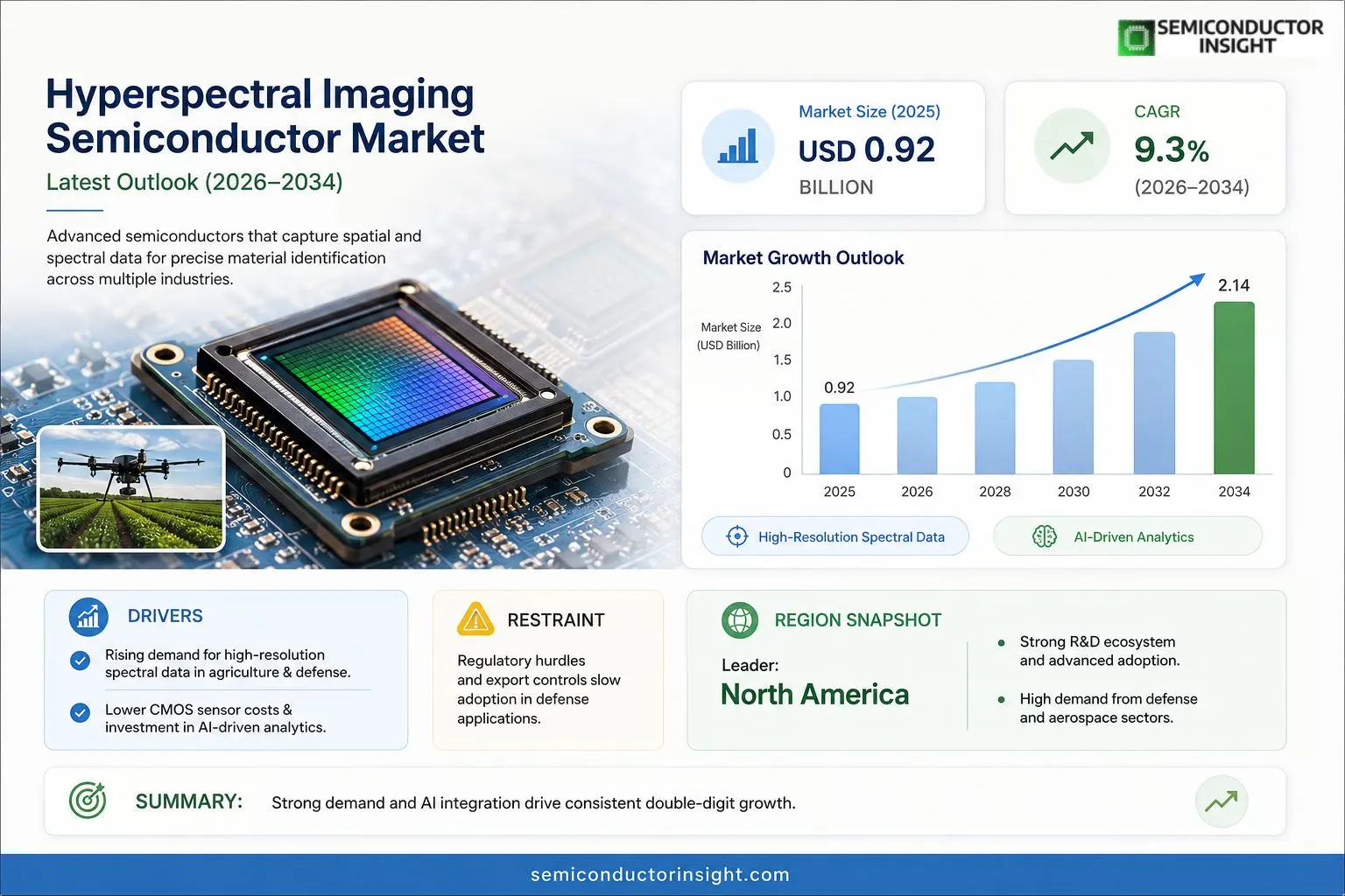
Global Hyperspectral Imaging Semiconductor Market size was valued at USD 0.92 billion in 2025. The market is projected to grow from USD 0.98 billion in 2026 to USD 2.14 billion by 2034, exhibiting a CAGR of 9.3% during the forecast period.
Hyperspectral imaging semiconductors are advanced photonic chips that enable simultaneous capture of spatial and spectral information across dozens to hundreds of contiguous wavelength bands. These devices integrate focal‑plane arrays with on‑chip dispersion elements or filter‑stack architectures, allowing precise material identification, chemical mapping, and quantitative analysis in applications ranging from remote sensing to medical diagnostics.The market is experiencing rapid growth because of expanding demand for high‑resolution spectral data in agriculture, defense, and industrial quality control. Furthermore, decreasing fabrication costs of CMOS‑based sensor platforms and increased investment in AI‑driven analytics are accelerating adoption. Key players such as Sony Corporation, Hamamatsu Photonics, Teledyne e2v, and ON Semiconductor are launching next‑generation hyperspectral sensor lines and forming strategic partnerships with aerospace firms to broaden deployment.
MARKET DRIVERS
Rising Demand in Precision Agriculture
Hyperspectral Imaging Semiconductor Market is being propelled by the need for high‑resolution crop monitoring, which enables farmers to detect disease, nutrient deficiencies, and water stress earlier than conventional methods. This early detection drives higher yield efficiency and reduces input costs, encouraging adoption of hyperspectral sensors across large‑scale farming operations.
Expansion in Remote Sensing and Surveillance
Governments and commercial entities are investing heavily in satellite‑based and UAV‑mounted hyperspectral platforms for environmental monitoring, border security, and disaster management. The ability to differentiate materials at a molecular level offers a strategic advantage that fuels demand for advanced semiconductor components.
➤ Industry analysts project a sustained double‑digit annual growth rate for the hyperspectral segment, driven primarily by agricultural and defense applications.
Overall, the convergence of digital agriculture, smart cities, and security imperatives creates a robust growth engine for Hyperspectral Imaging Semiconductor Market, ensuring continued investment in research and manufacturing capabilities.
MARKET CHALLENGES
High Development and Integration Costs
Designing hyperspectral sensors requires sophisticated semiconductor processes, precision optics, and extensive calibration, which together result in capital‑intensive projects. Small and medium‑sized enterprises often face budget constraints that limit their ability to adopt the latest technology.
Other Challenges
Supply Chain Constraints
The reliance on rare‑earth materials and specialized fabrication facilities creates vulnerability to geopolitical tensions and raw‑material shortages, potentially delaying product rollouts.
MARKET RESTRAINTS
Regulatory Hurdles in Defense Applications
Stringent export controls and defense‑related certification processes can slow market entry for hyperspectral semiconductor solutions, especially when cross‑border collaborations are required. Compliance costs and lengthy approval cycles act as a restraint on rapid market expansion.
MARKET OPPORTUNITIES
Integration with AI‑Enabled Analysis Tools
The fusion of hyperspectral data with artificial intelligence and machine‑learning algorithms opens new avenues for real‑time decision making in sectors such as food safety, mineral exploration, and medical diagnostics. This synergy presents a high‑growth opportunity for semiconductor manufacturers that can deliver optimized, AI‑ready sensor platforms.
Hyperspectral Imaging Semiconductor Market Trends
Growth Driven by High‑Resolution Spectral Demand
Hyperspectral Imaging Semiconductor Market is experiencing accelerated expansion as industries require more detailed spectral information. The market was valued at USD 0.92 billion in 2025, rose to USD 0.98 billion in 2026, and is projected to reach USD 2.14 billion by 2034. This growth is fueled by agricultural monitoring, defense surveillance, and industrial quality control, all of which benefit from advanced photonic chips that capture dozens to hundreds of contiguous wavelength bands in a single exposure. The decreasing fabrication costs of CMOS‑based sensor platforms, combined with heightened investment in AI‑driven analytics, have lowered barriers to entry and broadened adoption across midsize enterprises. Leading vendors such as Sony Corporation, Hamamatsu Photonics, Teledyne e2v, and ON Semiconductor are continuously launching next‑generation hyperspectral sensor lines, integrating on‑chip dispersion elements and filter‑stack architectures to improve material identification accuracy and quantitative analysis capabilities.
Other Trends
Integration of AI for Real‑Time Analysis
Manufacturers are embedding AI inference engines directly on sensor platforms, enabling on‑device classification of crops, detection of hazardous chemicals, and rapid defect inspection in manufacturing lines. This on‑chip AI reduces data transfer latency, minimizes the need for separate processing hardware, and supports autonomous decision‑making in UAVs and portable diagnostic devices. As a result, customers can achieve near‑instant insights, driving higher operational efficiency and reinforcing the value proposition of hyperspectral imaging semiconductors in time‑critical applications.
Strategic Partnerships Expanding Market Reach
Key players are forging strategic alliances with aerospace manufacturers, automotive OEMs, and medical device firms to embed hyperspectral sensors into satellite payloads, advanced driver‑assistance systems, and point‑of‑care imaging equipment. These collaborations accelerate deployment cycles, provide access to diversified end‑user ecosystems, and create new revenue streams that extend beyond traditional remote‑sensing markets. Joint development programs also focus on miniaturizing sensor arrays and enhancing ruggedness, which opens opportunities in field‑deployed military platforms and on‑site agricultural drones. The cumulative effect of these partnerships is a broader market footprint and a more resilient demand base for Hyperspectral Imaging Semiconductor Market through the end of the forecast horizon.
COMPETITIVE LANDSCAPEKey Industry Players
Competitive Overview of the Global Hyperspectral Imaging Semiconductor Market
The hyperspectral imaging semiconductor segment is dominated by a handful of vertically integrated manufacturers that combine advanced CMOS process capabilities with proprietary dispersion architectures. Sony Corporation leverages its extensive image sensor portfolio to deliver high‑resolution focal‑plane arrays that support dozens of spectral bands, while Hamamatsu Photonics distinguishes itself through ultra‑low noise photonic chips tailored for medical diagnostics. Teledyne e2v (part of Teledyne) and ON Semiconductor (onsemi) focus on rugged, aerospace‑qualified modules that integrate on‑chip filter stacks, enabling precise material discrimination for defense and remote‑sensing applications. These incumbents collectively control a majority of the high‑volume supply chain, dictating pricing trends and setting performance benchmarks for the market projected to reach $2.14 billion by 2034.Beyond the core tier, a vibrant ecosystem of niche innovators expands the technology’s reach into specialized domains. Xenics and Himax Technologies develop compact CMOS‑based hyperspectral sensors targeting industrial quality control and agricultural monitoring. Sensors Unlimited (Collins Aerospace) and FLIR Systems (Teledyne FLIR) offer custom solutions for unmanned aerial systems, while Quintessential Imaging and Norsonic concentrate on spectroscopy for environmental and chemical analysis. Emerging entrants such as LumaSense Technologies, STMicroelectronics, and Samsung Electronics are investing in next‑generation on‑chip dispersion techniques, positioning themselves to capture market share as AI‑driven analytics increase demand for high‑fidelity spectral data.
List of Key Hyperspectral Imaging Semiconductor Companies Profiled
- Sony Corporation
- Hamamatsu Photonics
- Teledyne e2v
- ON Semiconductor (onsemi)
- Himax Technologies
- Xenics
- Sensors Unlimited (Collins Aerospace)
- FLIR Systems (Teledyne FLIR)
- Quintessential Imaging
- Norsonic
- LumaSense Technologies
- STMicroelectronics
- Samsung Electronics
- Toshiba Corporation
Segment Analysis:
| Segment Category | Sub-Segments | Key Insights |
| By Type |
|
Focal‑Plane Array Sensors are emerging as the dominant type because they enable high‑resolution spatial‑spectral capture on a single chip, supporting compact system designs and fast data acquisition.
|
| By Application |
|
Agriculture drives adoption as hyperspectral data enables precise crop health monitoring, nutrient mapping, and early pest detection.
|
| By End User |
|
OEMs are pivotal because they embed hyperspectral chips directly into end‑products, creating differentiated value propositions.
|
| By Technology |
|
CMOS‑based Sensors dominate due to their lower power consumption, integration flexibility, and compatibility with standard semiconductor fabs.
|
| By Integration Mode |
|
Embedded Systems are gaining attention as manufacturers embed hyperspectral chips directly into machinery, enabling on‑board analysis.
|
Regional Analysis: North America
North America
The defense sector in North America is actively seeking hyperspectral imaging solutions for enhanced surveillance and target identification. Advanced aerospace applications are also benefiting from the improved spectral analysis capabilities offered by these semiconductor technologies.
North America’s focus on environmental sustainability is driving demand for hyperspectral imaging in areas like precision agriculture, water quality monitoring, and forest management. These technologies facilitate detailed analysis of environmental conditions.
The manufacturing sector in North America utilizes hyperspectral imaging for non-destructive testing, quality control, and defect detection in various industrial processes, enhancing efficiency and product reliability.
Emerging applications in healthcare, including disease detection and diagnostics, are leveraging the advanced spectral information provided by hyperspectral imaging semiconductors. Research initiatives are further expanding these possibilities.
North America
The North American market for **Hyperspectral Imaging Semiconductor Market** is characterized by significant private and public funding directed towards R&D initiatives. This commitment fosters continuous technological advancements, expanding the capabilities and applications of hyperspectral imaging. The strong presence of universities and research institutions contributes to a steady stream of innovative solutions. Businesses are increasingly adopting these technologies to gain deeper insights into materials and processes, leading to enhanced decision-making.
Europe
Europe represents a substantial and growing market for **Hyperspectral Imaging Semiconductor Market**. Strong emphasis on environmental protection and industrial efficiency is propelling adoption across various sectors. Several European countries are actively investing in hyperspectral imaging for applications in agriculture, pharmaceuticals, and materials science. The region’s collaborative research environment further accelerates technological development.
Asia-Pacific
Asia-Pacific is emerging as a key region for the **Hyperspectral Imaging Semiconductor Market**, driven by rapid industrialization and increasing investments in technological innovation. Countries like China and Japan are leading the adoption of hyperspectral imaging in sectors such as manufacturing, defense, and environmental monitoring. The expanding electronics industry in the region also presents significant opportunities.
South America
South America presents a developing market for **Hyperspectral Imaging Semiconductor Market**, primarily driven by agricultural advancements and resource exploration. The region’s extensive agricultural lands are benefiting from precision agriculture techniques enabled by hyperspectral imaging. However, market adoption is relatively nascent compared to other regions, with significant growth potential.
Middle East & Africa
The Middle East & Africa region showcases a promising, albeit emerging, market for the **Hyperspectral Imaging Semiconductor Market**. Growing investments in infrastructure development, oil and gas exploration, and defense applications are fueling demand. The focus on resource management and environmental monitoring further contributes to market growth in this region.
Report Scope
This market research report provides a comprehensive analysis of the Hyperspectral Imaging Semiconductor Market , covering the forecast period 2026–2034. It offers detailed insights into market dynamics, technological advancements, competitive landscape, and key trends shaping the industry.
Key focus areas of the report include:
- Market Overview: The report begins with an overview outlining its current market scenario, key growth indicators, and industry transformation drivers. It discusses macroeconomic factors, demand–supply balance, regulatory landscape, and the strategic role of semiconductors in powering advancements across industries such as automotive, telecommunications, consumer electronics, and industrial automation.
- Market Size & Forecast: Historical data and future projections for revenue, unit shipments, and market value across major regions and segments.
- Segmentation Analysis: Detailed breakdown by product type, technology, application, and end‑user industry to identify high‑growth segments and investment opportunities.
- Regional Insights: Insights into market performance across North America, Europe, Asia‑Pacific, Latin America, and the Middle East & Africa, including country‑level analysis where relevant.
- Competitive Landscape: Profiles of leading market participants, including their product offerings, R&D focus, manufacturing capacity, pricing strategies, and recent developments such as mergers, acquisitions, and partnerships.
- Technology Trends & Innovation: Assessment of emerging technologies, integration of AI/IoT, semiconductor design trends, fabrication techniques, and evolving industry standards.
- Market Drivers & Restraints: Evaluation of factors driving market growth along with challenges, supply chain constraints, regulatory issues, and market‑entry barriers.
- Stakeholder Insights: Insights for component suppliers, OEMs, system integrators, investors, and policymakers regarding the evolving ecosystem and strategic opportunities.
Primary and secondary research methods are employed, including interviews with industry experts, data from verified sources, and real‑time market intelligence to ensure the accuracy and reliability of the insights presented.
FREQUENTLY ASKED QUESTIONS:
What is the current market size of Hyperspectral Imaging Semiconductor Market?
-> Hyperspectral Imaging Semiconductor Market was valued at USD 0.92 billion in 2025 and is expected to reach USD 2.14 billion by 2034, reflecting a CAGR of 9.3 % over the forecast period.
Which key companies operate in Hyperspectral Imaging Semiconductor Market?
-> Key players include Sony Corporation, Hamamatsu Photonics, Teledyne e2v, and ON Semiconductor, among others.
What are the key growth drivers?
-> Key growth drivers include rising demand for high‑resolution spectral data in agriculture, defense, and industrial quality control, decreasing CMOS sensor fabrication costs, and increased investment in AI‑driven analytics.
Which region dominates the market?
-> The reference does not specify a dominant region.
What are the emerging trends?
-> Emerging trends include integration of hyperspectral sensors with AI/IoT platforms, development of compact CMOS‑based focal‑plane arrays, and expanding applications in medical diagnostics and remote sensing.
Get Sample Report PDF for Exclusive Insights
Report Sample Includes
- Table of Contents
- List of Tables & Figures
- Charts, Research Methodology, and more...
 Download Sample Report PDF


