Hybrid bonding 3D NAND with CMOS under array chip Market Insights
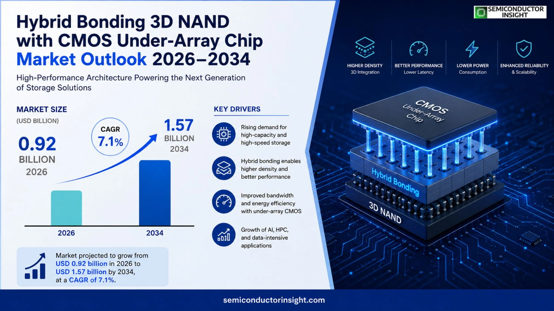
Global Hybrid bonding 3D NAND with CMOS under‑array chip market size was valued at USD 0.84 billion in 2025. The market is projected to grow from USD 0.92 billion in 2026 to USD 1.57 billion by 2034, exhibiting a CAGR of 7.1% during the forecast period.
This technology integrates three‑dimensional NAND flash memory stacks directly onto a CMOS logic substrate using wafer‑level hybrid bonding, eliminating traditional interconnects and enabling sub‑10 µm pitch interconnects with superior electrical performance and thermal stability.
The market is accelerating because leading semiconductor manufacturers are seeking higher storage density and lower power consumption for AI‑enabled edge devices, while advances in low‑temperature plasma activation improve bond yield. Furthermore, major players such as Samsung, SK Hynix and Intel have announced roadmaps that prioritize hybrid‑bonded architectures, reinforcing confidence in sustained growth.
MARKET DRIVERS
Rising Demand for High‑Performance Storage
Hybrid bonding 3D NAND with CMOS under array chip Market is being propelled by exponential growth in data‑intensive workloads such as cloud computing, edge AI and autonomous systems. Enterprises are seeking memory solutions that deliver higher bandwidth per pin and lower power consumption, which traditional planar NAND cannot satisfy.
Advancements in Hybrid Bonding Technology
Recent breakthroughs in wafer‑level bonding have reduced interconnect resistance to below 1 mΩ·cm², enabling tighter integration of NAND stacks with CMOS logic. This technical progression shortens signal latency and supports multi‑gigabyte per second data rates, reinforcing the commercial case for adopting hybrid‑bonded architectures.
➤ Analysts estimate that hybrid‑bonded solutions could capture up to 30% of the premium NAND segment by 2028, driven by their superior performance‑per‑watt metrics.
As device manufacturers prioritize miniaturization, the compact form factor offered by hybrid bonding aligns with the industry’s roadmap to sub‑20 nm node integration, further accelerating market adoption.
MARKET CHALLENGES
Manufacturing Yield Constraints
Yield optimization remains a critical hurdle because the hybrid bonding process demands sub‑nanometer surface planarity and precise alignment. Any deviation can lead to defect propagation across the stacked layers, inflating production costs and delaying time‑to‑market.
Other Challenges
Cost Sensitivity
Despite performance gains, the higher capital expenditure for specialized equipment makes manufacturers wary, especially when price‑sensitive consumer segments dominate the broader NAND market.
MARKET RESTRAINTS
Supply Chain Vulnerabilities
The reliance on a limited number of semiconductor foundries equipped for hybrid bonding intensifies supply‑chain risk. Geopolitical tensions and material shortages can therefore constrain scaling efforts and impact overall market growth.
MARKET OPPORTUNITIES
Emerging AI‑Driven Applications
AI inference engines and next‑generation graphics processors require ultra‑fast, high‑density memory. Hybrid bonding 3D NAND paired with CMOS under‑array chips delivers the requisite bandwidth and energy efficiency, presenting a sizable growth avenue as AI workloads continue to expand across industries.
Hybrid bonding 3D NAND with CMOS under array chip Market Trends
Advances in Hybrid Bonding Technology
The industry is witnessing a rapid shift toward wafer‑level hybrid bonding that directly attaches three‑dimensional NAND memory stacks onto CMOS logic substrates. This approach eliminates traditional interconnect layers, delivering sub‑10 µm pitch connections with markedly lower parasitic resistance and improved thermal performance. As AI‑enabled edge devices demand higher storage density and lower power draw, the technology’s ability to retain signal integrity at tighter pitches is becoming a decisive competitive factor.
Other Trends
Manufacturing Yield Improvements
Low‑temperature plasma activation has emerged as a critical enabler, raising bond yield by reducing particle contamination and surface roughness. Leading fabs report consistent yield gains that translate into shorter cycle times and lower defect-related costs. The convergence of advanced surface preparation and real‑time metrology is also driving tighter process windows, reinforcing confidence among equipment suppliers and design houses.
Strategic Roadmaps of Major Players
Key semiconductor manufacturers such as Samsung, SK Hynix and Intel have incorporated hybrid‑bonded architectures into their multi‑year product roadmaps. Their public statements emphasize a focus on integrating high‑capacity NAND flash with high‑performance logic to meet the projected demand from data‑center accelerators and autonomous‑vehicle platforms. By aligning R&D investments with this technology, these firms are positioning themselves to capture a larger share of Hybrid bonding 3D NAND with CMOS under array chip Market as adoption expands.
Overall, the market trajectory reflects a blend of technical maturation and strategic commitment. The reduction in interconnect overhead, combined with measurable gains in thermal stability, is enabling device designers to push storage capacities beyond traditional scaling limits. As ecosystem partnerships deepen and supply‑chain confidence grows, the sector is poised for sustained growth while maintaining a disciplined focus on yield, reliability, and cost efficiency.
COMPETITIVE LANDSCAPE
Key Industry Players
Hybrid bonding 3D NAND with CMOS under‑array chip market competitive overview
Hybrid‑bonded 3D NAND‑CMOS under‑array segment is currently dominated by three global leaders,Samsung Electronics, SK Hynix, and Intel Corporation,whose road‑maps explicitly commit multi‑year investments in wafer‑level hybrid bonding. Samsung’s use of its advanced “X‑Band” process and SK Hynix’s recent 176‑layer NAND demonstration illustrate a clear consolidation around high‑density, sub‑10 µm pitch interconnects. Intel leverages its “Foveros” 3D integration platform to pair logic and storage in a single stack, delivering superior thermal performance for AI‑edge workloads. This triad shapes a market structure where scale, proprietary bonding chemistries, and deep vertical integration differentiate the leaders from the rest of the ecosystem, driving a projected CAGR of 7.1 % through 2034.
Beyond the three marquee firms, a broader cohort of niche but strategically important players contributes critical process equipment, packaging services, and specialty memory IP. Companies such as Micron Technology and Kioxia (formerly Toshiba Memory) are accelerating hybrid‑bonded product pilots, while foundries like TSMC and GlobalFoundries enable third‑party access to mature bonding lines. Packaging specialists,including ASE Technology Holding, Amkor Technology, and JCET,provide advanced redistribution layers that complement hybrid bonding die‑to‑die connections. Supportive ecosystem players such as Texas Instruments, Infineon Technologies, and Applied Materials supply the analog front‑end, power‑management ICs, and plasma‑activation tools essential for high‑yield production. These diverse contributors collectively reinforce supply‑chain resilience and foster incremental innovation across the value chain.
List of Key Hybrid Bonding 3D NAND with CMOS Under‑Array Chip Companies Profiled
- Samsung Electronics
- SK Hynix
- Intel Corporation
- Micron Technology
- Kioxia (Toshiba Memory)
- TSMC
- GlobalFoundries
- ASE Technology Holding
- Amkor Technology
- JCET Group
- Texas Instruments
- Infineon Technologies
- Applied Materials
- Lam Research
- NXP Semiconductors
Segment Analysis:
| Segment Category | Sub-Segments | Key Insights |
| By Type |
|
Hybrid‑Bonded 3D NAND with CMOS Logic
|
| By Application |
|
AI Edge Accelerators
|
| By End User |
|
Data Center Servers
|
| By Integration Approach |
|
Wafer‑Level Hybrid Bonding
|
| By Technology Maturity |
|
Growth Phase
|
Regional Analysis: North America
The data center sector in North America is a primary driver for Hybrid bonding 3D NAND adoption. The high bandwidth and capacity requirements of modern data centers necessitate advanced memory solutions, making this technology a key enabler for improved performance and efficiency.
The consumer electronics market in North America, encompassing smartphones, laptops, and gaming consoles, is witnessing a steady shift towards higher storage capacities, thereby boosting the demand for Hybrid bonding 3D NAND with CMOS under array chip.
The automotive industry’s increasing reliance on in-vehicle infotainment systems, advanced driver-assistance systems (ADAS), and autonomous driving technologies is creating new opportunities for Hybrid bonding 3D NAND adoption.
North America’s strong HPC sector is actively exploring and implementing Hybrid bonding 3D NAND to meet the demanding memory requirements of complex computational tasks and scientific simulations.
Europe
The European market for Hybrid bonding 3D NAND with CMOS under array chip is characterized by a strong emphasis on energy efficiency and data security. Stringent data privacy regulations and a growing focus on sustainable technologies are shaping the market dynamics in the region. Key applications include the automotive industry, industrial IoT, and enterprise data storage. The adoption rate is steadily increasing as European manufacturers seek to enhance the performance and capacity of their products while adhering to environmental standards. The rise of edge computing initiatives also contributes to the demand for high-performance memory solutions in Europe.
Asia-Pacific
Asia-Pacific is the largest and fastest-growing market for Hybrid bonding 3D NAND with CMOS under array chip. The region’s burgeoning electronics manufacturing hubs, particularly in China, South Korea, and Taiwan, are major contributors to this growth. The increasing demand for smartphones, cloud computing infrastructure, and electric vehicles fuels the adoption of this advanced memory technology. Government initiatives promoting semiconductor industry development and significant investments in R&D further accelerate market expansion. Competitive pressures are intense, with numerous regional and global players vying for market share.
South America
The South American market for Hybrid bonding 3D NAND with CMOS under array chip is relatively nascent but exhibits promising growth potential. The expanding telecommunications infrastructure, increasing adoption of cloud services, and a growing consumer electronics market are driving demand. The region is witnessing a gradual shift towards higher storage capacities and improved performance in various applications. However, economic uncertainties and infrastructure limitations pose some challenges to market growth.
Middle East & Africa
The Middle East and Africa represent a smaller but emerging market for Hybrid bonding 3D NAND with CMOS under array chip. The growth is primarily driven by increasing investments in digital transformation initiatives, expanding data center capacity, and rising demand for consumer electronics. The region’s focus on smart city development and the adoption of IoT technologies are also contributing factors. While the market is still in its early stages, it holds considerable potential for future growth as infrastructure development progresses.
Report Scope
This market research report provides a comprehensive analysis of the Hybrid bonding 3D NAND with CMOS under array chip Market , covering the forecast period 2026–2034. It offers detailed insights into market dynamics, technological advancements, competitive landscape, and key trends shaping the industry.
Key focus areas of the report include:
- Market Overview: The report begins with an overview outlining its current market scenario, key growth indicators, and industry transformation drivers. It discusses macroeconomic factors, demand–supply balance, regulatory landscape, and the strategic role of semiconductors in powering advancements across industries such as automotive, telecommunications, consumer electronics, and industrial automation.
- Market Size & Forecast: Historical data and future projections for revenue, unit shipments, and market value across major regions and segments.
- Segmentation Analysis: Detailed breakdown by product type, technology, application, and end-user industry to identify high-growth segments and investment opportunities.
- Regional Insights: Insights into market performance across North America, Europe, Asia-Pacific, Latin America, and the Middle East & Africa, including country-level analysis where relevant.
- Competitive Landscape: Profiles of leading market participants, including their product offerings, R&D focus, manufacturing capacity, pricing strategies, and recent developments such as mergers, acquisitions, and partnerships.
- Technology Trends & Innovation: Assessment of emerging technologies, integration of AI/IoT, semiconductor design trends, fabrication techniques, and evolving industry standards.
- Market Drivers & Restraints: Evaluation of factors driving market growth along with challenges, supply chain constraints, regulatory issues, and market-entry barriers.
- Stakeholder Insights: Insights for component suppliers, OEMs, system integrators, investors, and policymakers regarding the evolving ecosystem and strategic opportunities.
Primary and secondary research methods are employed, including interviews with industry experts, data from verified sources, and real-time market intelligence to ensure the accuracy and reliability of the insights presented.
FREQUENTLY ASKED QUESTIONS:
What is the current market size of Hybrid bonding 3D NAND with CMOS under array chip Market?
-> Hybrid bonding 3D NAND with CMOS under array chip Market was valued at USD 0.84 billion in 2025 and is expected to reach USD 1.57 billion by 2034.
Which key companies operate Hybrid bonding 3D NAND with CMOS under array chip Market?
-> Key players include Samsung, SK Hynix, Intel, among others.
What are the key growth drivers?
-> Key growth drivers include higher storage density demands, lower power consumption for AI‑enabled edge devices, and advances in low‑temperature plasma activation improving bond yield.
Which region dominates the market?
-> Asia-Pacific is the fastest‑growing region, while North America remains a dominant market.
What are the emerging trends?
-> Emerging trends include integration of hybrid‑bonded architectures in AI edge computing, development of sub‑10 µm pitch interconnects, and roadmap commitments from major semiconductor manufacturers.

Get Sample Report PDF for Exclusive Insights
Report Sample Includes
- Table of Contents
- List of Tables & Figures
- Charts, Research Methodology, and more...


