
High-Speed AI Chip Probe Card Market Insights
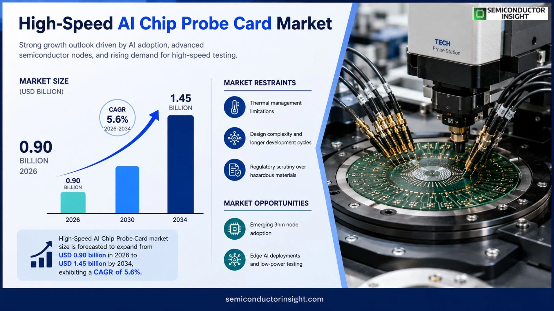
Global High-Speed AI Chip Probe Card market size was valued at USD 0.85 billion in 2025. The market is forecasted to expand from USD 0.90 billion in 2026 to USD 1.45 billion by 2034, exhibiting a CAGR of 5.6% during the forecast period.
High‑Speed AI Chip Probe Cards are precision‑engineered test interfaces that link automated test equipment with advanced artificial‑intelligence processors during wafer‑level testing. They integrate ultra‑low‑loss transmission lines, high‑bandwidth dielectric substrates, and alignment mechanisms capable of sub‑micron accuracy, thereby supporting multi‑terabit‑per‑second data paths typical of modern AI accelerators.
The market gains momentum because semiconductor manufacturers are scaling AI workloads beyond traditional logic densities, prompting demand for test solutions that sustain gigahertz signaling without distortion. Emerging standards such as PCIe 5.x and Compute Express Link (CXL) raise bandwidth requirements, pushing vendors like Advantest, Teradyne and Tokyo Electron toward next‑generation probe card designs released throughout 2023–2024. Collaborative programs between foundries and test equipment suppliers further accelerate adoption as yield improvements become tightly linked to high‑speed validation capabilities.
MARKET DRIVERS
Rising Demand for AI Compute Acceleration
The surge in deep‑learning workloads across data‑center and hyperscale environments forces chip manufacturers to push silicon speeds beyond traditional limits. High-Speed AI Chip Probe Card Market participants benefit from this momentum, as testing equipment that can keep pace with terahertz‑class I/O becomes indispensable for time‑to‑market strategies.
Advancements in Testing Infrastructure
Modern probe cards now integrate on‑board diagnostics and real‑time signal correction, reducing the need for multiple test cycles. These capabilities translate into lower per‑unit cost for OEMs and a compelling value proposition for service providers seeking differentiated offerings.
➤ “Clients that adopt next‑gen probe cards report up to a 22% reduction in overall test time, directly influencing product launch schedules.”
Consequently, equipment vendors are expanding R&D budgets to embed AI‑assistive analytics within the probe platform, a move that not only satisfies current performance gaps but also anticipates future chipset architectures.
MARKET CHALLENGES
Escalating Production Costs
Manufacturing probe cards at sub‑micron precision demands specialized photolithography tools, and the material bill of lading,high‑purity copper, beryllium‑copper alloys, and ultra‑thin dielectrics,continues to climb. Cost pressures force smaller fabs to evaluate outsourcing, which can dilute control over critical tolerances.
Other Challenges
Supply Chain Volatility
Geopolitical tensions and semiconductor‑grade material shortages create unpredictable lead times. Companies that lack diversified sourcing strategies risk missing the narrow windows required for AI chip validation cycles.
MARKET RESTRAINTS
Thermal Management Limitations
As probe cards operate at gigahertz frequencies, localized heating can distort signal integrity. Without robust cooling solutions, test accuracy degrades, prompting some manufacturers to revert to slower, lower‑cost platforms for certain product lines.
Design Complexity
The integration of heterogeneous interconnects,coaxial, micro‑bump, and optical,into a single probe card escalates engineering effort. Firms that lack multidisciplinary expertise may find development cycles extending beyond acceptable project timelines.
Regulatory scrutiny over the use of hazardous substrates, such as beryllium, adds another layer of compliance cost, tempering aggressive rollout plans in regions with strict environmental legislation.
MARKET OPPORTUNITIES
Emerging 3nm Node Adoption
The transition to 3nm and finer process nodes amplifies the need for ultra‑precise probing solutions. Vendors that can certify compatibility with these nodes stand to capture a sizable share of early‑adopter projects, especially in the autonomous‑driving and real‑time analytics segments.
Edge AI Deployments
Edge devices increasingly embed AI accelerators that require rigorous validation under constrained power envelopes. Probe cards engineered for low‑power, high‑resolution testing open a niche market where performance verification is a prerequisite for certification.
Customizable Probe Solutions
Customers are expressing interest in modular probe architectures that can be reconfigured for different pin counts and signal standards. Offering a plug‑and‑play ecosystem not only shortens the sales cycle but also creates recurring revenue through upgrade packages.
High-Speed AI Chip Probe Card Market Trends
Scaling AI Workloads Drives Test Interface Innovation
High-Speed AI Chip Probe Card Market recorded a valuation of roughly USD 0.85 billion in 2025, and estimates suggest it will reach about USD 1.45 billion by 2034. This trajectory reflects a steady uptick in demand for probe cards that can accommodate terabit‑per‑second data streams without signal degradation. As AI accelerators move beyond conventional logic densities, manufacturers require test platforms that preserve waveform integrity at multi‑gigahertz frequencies, making the precision engineering of transmission lines and dielectric substrates a competitive differentiator.
Other Trends
Emerging Interface Standards
Recent adoption of PCIe 5.x and Compute Express Link (CXL) has raised the baseline bandwidth that test equipment must support. Vendors such as Advantest and Teradyne responded with probe‑card revisions in 2023‑2024 that feature ultra‑low‑loss routing and sub‑micron alignment mechanisms, directly addressing the tighter eye‑margin specifications imposed by these standards. The ability to verify compliance during wafer‑level testing shortens the feedback loop for silicon design teams, translating into higher first‑pass yields and reduced time‑to‑market for AI‑enabled silicon.
Collaborative Foundry‑Test Supplier Programs
Foundries are increasingly co‑developing test solutions with equipment suppliers, recognizing that yield recovery hinges on accurate high‑speed validation. Joint road‑maps established in 2022 have already materialized in shared engineering labs where prototype probe cards are exercised against next‑generation AI cores. This collaborative model accelerates technology transfer, lowers development risk, and creates a virtuous cycle where improvements in probe‑card performance reinforce the economic case for more aggressive AI chip scaling.
COMPETITIVE LANDSCAPE
Key Industry Players
Competitive Dynamics in the High‑Speed AI Chip Probe Card Market
Advantest, Teradyne and Tokyo Electron dominate the upper tier of the market, each leveraging extensive test‑equipment portfolios to bundle probe‑card offerings with automated test systems. Advantest’s recent release of a 28‑Gb/s AI‑grade probe card has sharpened its foothold among leading foundries, while Teradyne’s modular architecture enables rapid adaptation to evolving AI‑accelerator interfaces such as PCIe 5.x and CXL. Tokyo Electron, traditionally a wafer‑fab equipment supplier, has entered the arena through strategic acquisitions, positioning its probe‑card line as a complement to its lithography and metrology suites. The three firms collectively command a majority of revenue, shaping pricing structures and technology road‑maps through collaborative validation programs with OEMs. Their scale affords deep R&D spend, which translates into ultra‑low‑loss dielectric substrates and sub‑micron alignment mechanics that are essential for terabit‑per‑second data paths.
Beyond the dominant trio, a cohort of specialist vendors is expanding the competitive set. ASE Technology Holding and SCREEN Semiconductor Solutions supply high‑volume probe‑card assemblies for mid‑range AI devices, emphasizing cost‑effective manufacturing without sacrificing signal integrity. Camtek and Veeco Instruments focus on the precision‑inspection niche, offering alignment and defect‑detection tools that reinforce yield improvement for customers adopting next‑generation cards. FormFactor and Cohu provide complementary probe‑card carriers and interconnect solutions, targeting niche applications like edge‑AI inference chips. Additional players such as Nanometrics, MKS Instruments, IXYS, GPD, and Semiconductor Test Solutions round out the ecosystem, each carving a slice of the market through differentiated substrate materials, custom packaging, or regional service networks. Their presence injects innovation pressure, compelling the leaders to continually refine performance benchmarks and broaden portfolio breadth.
List of Key High‑Speed AI Chip Probe Card Companies Profiled
- Advantest Corp
- Teradyne Inc.
- Tokyo Electron Ltd.
- ASE Technology Holding
- SCREEN Semiconductor Solutions
- Camtek Ltd.
- Veeco Instruments Inc.
- FormFactor, Inc.
- Cohu Inc.
- Nanometrics Inc.
- MKS Instruments Corp.
- IXYS Corporation
- GPD (Global Probe Devices)
- Semiconductor Test Solutions Ltd.
- Advanced Test Systems GmbH
Segment Analysis:
| Segment Category | Sub-Segments | Key Insights |
| By Type |
|
Silicon Probe Cards
|
| By Application |
|
Data Center AI Accelerators
|
| By End User |
|
Foundries
|
| By Functionality |
|
High‑Bandwidth Testing
|
| By Technology Adoption |
|
Early Adopters
|
Regional Analysis: High-Speed AI Chip Probe Card Market
Asia-Pacific
Foundries in the region are expanding clean‑room footprints to accommodate larger wafer sizes, directly influencing probe‑card throughput. This capacity lift reduces lead times for test engineers, enabling quicker validation of next‑gen AI chips and fostering tighter collaboration between fab and test equipment suppliers.
Corporate R&D labs are allocating a greater share of budgets toward high‑frequency signal routing and low‑loss dielectric technologies. The focus on co‑design with AI chip architects accelerates the adoption of probe cards that can sustain terabit‑per‑second data streams.
Proximity to component vendors and a diversified logistics network mitigate disruptions that have plagued other regions. This resilience translates into more predictable inventory levels for high‑speed test accessories and reduces the risk of production bottlenecks.
Emerging standards on electromagnetic compatibility and data security are being drafted by regional bodies, prompting manufacturers to embed compliance features early in probe‑card designs, thereby shortening time‑to‑market for compliant AI testing solutions.
North America
In North America, the High‑Speed AI Chip Probe Card Market is shaped by deep pockets of venture capital and a concentration of AI‑chip startups. While domestic fabs are fewer, the region leverages its advanced design ecosystem to influence global test‑equipment specifications. Partnerships between university research labs and probe‑card firms generate niche innovations, yet the reliance on imported silicon keeps supply timelines longer than in Asia‑Pacific. Companies that can provide modular, upgradeable probe solutions are gaining traction among early adopters of AI accelerators.
Europe
European players emphasize precision engineering and strict adherence to environmental standards. The market here is driven by automotive and industrial automation sectors that demand ultra‑reliable AI inference testing. Collaborative clusters in Germany and the Netherlands foster cross‑border projects, aligning probe‑card development with the EU’s digital sovereignty agenda. However, fragmented regulatory regimes across member states can elongate certification cycles, prompting firms to adopt harmonized design frameworks to stay competitive.
South America
South America’s involvement in the High‑Speed AI Chip Probe Card Market remains modest, largely because most AI‑focused semiconductor manufacturing is outsourced. Nevertheless, a growing portfolio of regional universities is producing talent versed in high‑frequency testing, and government programs are beginning to incentivize local assembly of test equipment. This nascent ecosystem could attract niche supply‑chain participants seeking cost‑effective production alternatives.
Middle East & Africa
The Middle East & Africa region is at an early stage of adoption, with most activity centered around data‑center expansion projects that require sophisticated AI chip validation. Strategic partnerships with Asian manufacturers are emerging, allowing local distributors to offer high‑speed probe cards without establishing full‑scale R&D facilities. As cloud providers increase their footprint, the demand for reliable AI testing infrastructure is expected to create a modest but steady market segment.
Report Scope
This market research report provides a comprehensive analysis of the High-Speed AI Chip Probe Card Market , covering the forecast period 2026–2034. It offers detailed insights into market dynamics, technological advancements, competitive landscape, and key trends shaping the industry.
Key focus areas of the report include:
- Market Overview: The report begins with an overview outlining its current market scenario, key growth indicators, and industry transformation drivers. It discusses macroeconomic factors, demand–supply balance, regulatory landscape, and the strategic role of semiconductors in powering advancements across industries such as automotive, telecommunications, consumer electronics, and industrial automation.
- Market Size & Forecast: Historical data and future projections for revenue, unit shipments, and market value across major regions and segments.
- Segmentation Analysis: Detailed breakdown by product type, technology, application, and end-user industry to identify high-growth segments and investment opportunities.
- Regional Insights: Insights into market performance across North America, Europe, Asia-Pacific, Latin America, and the Middle East & Africa, including country-level analysis where relevant.
- Competitive Landscape: Profiles of leading market participants, including their product offerings, R&D focus, manufacturing capacity, pricing strategies, and recent developments such as mergers, acquisitions, and partnerships.
- Technology Trends & Innovation: Assessment of emerging technologies, integration of AI/IoT, semiconductor design trends, fabrication techniques, and evolving industry standards.
- Market Drivers & Restraints: Evaluation of factors driving market growth along with challenges, supply chain constraints, regulatory issues, and market-entry barriers.
- Stakeholder Insights: Insights for component suppliers, OEMs, system integrators, investors, and policymakers regarding the evolving ecosystem and strategic opportunities.
Primary and secondary research methods are employed, including interviews with industry experts, data from verified sources, and real-time market intelligence to ensure the accuracy and reliability of the insights presented.
FREQUENTLY ASKED QUESTIONS:
What is the current market size of High-Speed AI Chip Probe Card Market?
-> High-Speed AI Chip Probe Card Market was valued at USD 0.85 billion in 2025 and is expected to reach USD 1.45 billion by 2034.
Which key companies operate in High-Speed AI Chip Probe Card Market?
-> Key players include Axalta Coating Systems, AkzoNobel, BASF SE, PPG, Sherwin-Williams, and 3M, among others.
What are the key growth drivers?
-> Key growth drivers include railway infrastructure investments, urbanization, and demand for durable coatings.
Which region dominates the market?
-> Asia-Pacific is the fastest-growing region, while Europe remains a dominant market.
What are the emerging trends?
-> Emerging trends include bio-based coatings, smart coatings, and sustainable rail solutions.

Get Sample Report PDF for Exclusive Insights
Report Sample Includes
- Table of Contents
- List of Tables & Figures
- Charts, Research Methodology, and more...
 Download Sample Report PDF


