High-k Dielectrics Market Insights
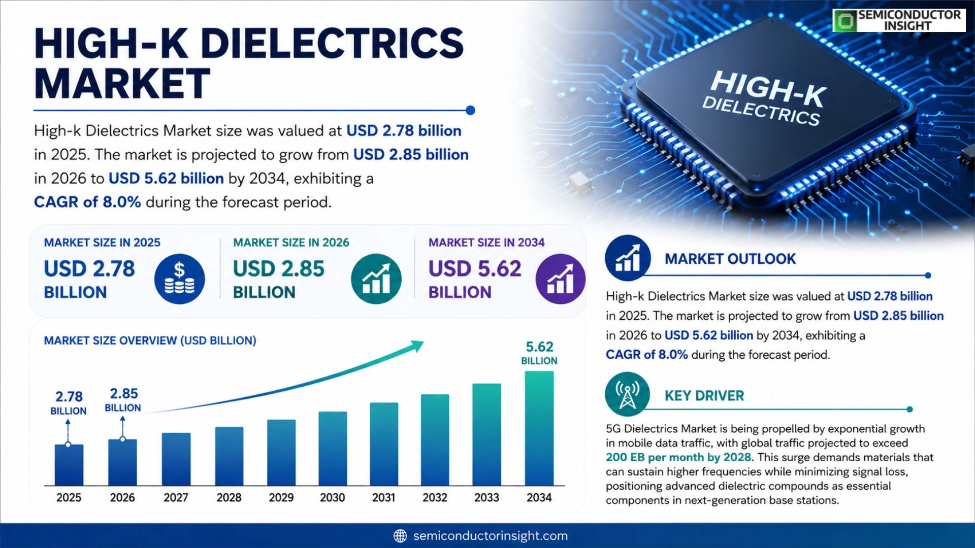
Global High‑k Dielectrics Market size was valued at USD 2.78 billion in 2025. The market is projected to grow from USD 2.85 billion in 2026 to USD 5.62 billion by 2034, exhibiting a CAGR of 8.0% during the forecast period.
High‑k dielectrics are materials with a dielectric constant (k) significantly higher than that of silicon dioxide, typically exceeding a k‑value of 10. They are employed as gate insulators in advanced CMOS transistors, as interlayer dielectrics in three‑dimensional integrated circuits, and in capacitors for power‑management applications because they enable reduced leakage current while maintaining capacitance scaling.
The market is accelerating because semiconductor manufacturers are pursuing sub‑3 nm nodes where traditional SiO₂ cannot meet leakage requirements; meanwhile, the proliferation of AI‑enabled edge devices and electric vehicles drives demand for energy‑efficient chips that rely on high‑k materials. Furthermore, recent collaborations,such as Intel’s integration of hafnium‑based high‑k dielectric into its latest process node announced in March 2024,demonstrate industry commitment to scaling performance while curbing power consumption.
MARKET DRIVERS
Technology Adoption in Advanced Nodes
High-k Dielectrics Market is being propelled by the rapid transition to sub‑10 nm semiconductor nodes, where traditional silicon dioxide can no longer meet leakage specifications. Manufacturers are adopting high‑k materials such as hafnium‑based compounds to sustain performance scaling, creating a clear demand surge.
Growth of Mobile and IoT Devices
Expanding smartphone penetration and the proliferation of IoT edge devices require power‑efficient chips. High‑k dielectrics enable lower operating voltages while preserving capacitance, making them a preferred choice for power‑management ICs in these segments.
➤ “The shift to high‑k materials is now a standard design rule for most leading‑edge fabs.”
In addition, government incentives for semiconductor reshoring are encouraging domestic fabs to invest in newer material stacks, further reinforcing the upward trajectory of High-k Dielectrics Market.
MARKET CHALLENGES
Manufacturing Complexity and Yield Concerns
Introducing high‑k layers adds additional process steps, such as atomic‑layer deposition and annealing cycles, which increase cycle time and require stringent control. Yield losses during early adoption phases can deter smaller fab operators.
Other Challenges
Cost Competitiveness
High‑k precursors are priced higher than conventional silicon dioxide, and the overall cost of the dielectric stack can impact the total cost of ownership for volume production.
MARKET RESTRAINTS
Material Compatibility Issues
Some high‑k compounds exhibit undesirable reactions with copper interconnects, leading to reliability concerns such as time‑dependent dielectric breakdown. Mitigating these interactions often requires additional barrier layers, adding design complexity.
Thermal stability remains a restraint; certain high‑k materials degrade at temperatures common in advanced back‑end processes, limiting their applicability in high‑performance logic devices.
Regulatory scrutiny over the use of rare‑earth elements in some high‑k formulations also introduces supply‑chain uncertainty, affecting long‑term planning for manufacturers.
MARKET OPPORTUNITIES
Emerging 3D Integration Technologies
Three‑dimensional stacking of memory and logic components demands ultra‑thin, high‑k dielectrics to manage inter‑layer coupling. This creates a niche where High-k Dielectrics Market can capture significant value through specialized material solutions.
Advanced packaging, such as fan‑out wafer‑level packaging, also relies on high‑k dielectrics to achieve fine pitch interconnects while controlling parasitic capacitance, opening new revenue streams for material suppliers.
Finally, the rise of quantum‑computing research is exploring high‑k oxides as gate dielectrics for novel transistor architectures, presenting a frontier growth area that may shape the next decade of the market.
High-k Dielectrics Market Trends
Scaling to Sub‑3 nm Nodes
The semiconductor industry is rapidly moving toward sub‑3 nm technology nodes, where traditional silicon dioxide gate insulators cannot meet the stringent leakage specifications required for high‑performance logic. High‑k dielectrics, defined by a dielectric constant (k) greater than 10, provide the necessary capacitance scaling while suppressing leakage currents. This shift is reshaping High-k Dielectrics Market as chip manufacturers prioritize materials that sustain power‑efficiency without sacrificing transistor density. The transition to advanced nodes is also driving increased adoption of hafnium‑based compounds, which have demonstrated superior thermal stability and dielectric strength in recent pilot productions.
Other Trends
AI‑Enabled Edge Devices
AI‑driven edge computing and electric‑vehicle power‑management systems demand chips that operate with minimal energy loss. High‑k dielectric layers are integral to the power‑management capacitors and interlayer dielectrics that enable these devices to meet both performance and power‑budget constraints. As the volume of edge devices expands, High‑k Dielectrics Market experiences a parallel rise in demand for materials that support high‑frequency operation and low‑temperature processing, ensuring seamless integration into diverse form factors.
Strategic Collaborations and Material Innovation
Recent industry collaborations underscore the strategic importance of material innovation with High‑k Dielectrics Market. Intel’s announcement in March 2024 of a hafnium‑based high‑k dielectric integration into its latest process node illustrates a concrete commitment to scaling performance while curbing power consumption. Similar partnerships between foundries and specialty material suppliers are accelerating the development of novel dielectric stacks that combine high k‑values with improved reliability. These alliances not only shorten the time‑to‑market for next‑generation chips but also create a feedback loop that fuels ongoing research, further solidifying the market’s growth trajectory.
COMPETITIVE LANDSCAPE
Key Industry Players
High‑k Dielectrics Market Competitive Landscape – 2024
High‑k Dielectrics Market is dominated by a small number of vertically integrated semiconductor giants that control both the design of advanced nodes and the sourcing of hafnium‑based materials. Intel leads the landscape, having announced the integration of a hafnium‑based high‑k gate stack into its 3‑nm process in early 2024, a move that signals a strategic commitment to material innovation to meet sub‑3 nm leakage targets. Samsung Electronics follows closely, leveraging its massive fab capacity to qualify high‑k films across its 4‑nm and 3‑nm product lines, while Taiwan Semiconductor Manufacturing Co. (TSMC) solidifies its position by partnering with leading material suppliers to secure a reliable supply chain for high‑k dielectric precursors. These three firms shape the market structure by dictating volume demand, setting price benchmarks, and driving collaborative research that raises the technological bar for the entire ecosystem.
Beyond the tier‑one players, a cohort of niche but highly specialized companies contributes critical capabilities in material synthesis, deposition equipment, and process integration. SK Hynix, GlobalFoundries, and Micron Technology invest in in‑house R&D to adapt high‑k solutions for memory and storage products, expanding the application scope beyond logic. Applied Materials and ASM International supply atomic‑layer‑deposition (ALD) tools essential for conformal high‑k film formation, while material innovators such as STMicroelectronics, Infineon Technologies, and NXP Semiconductors focus on automotive and IoT segments where power‑efficient high‑k dielectrics are increasingly required. Regional players including Texas Instruments, ROHM Semiconductor, and UMC add diversity to the supply base, ensuring that emerging edge‑computing and electric‑vehicle chip designs have access to verified high‑k solutions.
List of Key High‑k Dielectrics Market Companies Profiled
- Intel
- Samsung Electronics
- Taiwan Semiconductor Manufacturing Co.
- SK Hynix
- GlobalFoundries
- Applied Materials
- ASM International
- STMicroelectronics
- Infineon Technologies
- NXP Semiconductors
- Texas Instruments
- Micron Technology
- ROHM Semiconductor
- UMC
- Qorvo
Segment Analysis:
| Segment Category | Sub-Segments | Key Insights |
| By Type |
|
Hafnium‑based Dielectrics are the dominant choice because they combine high dielectric constant with thermal stability, enabling aggressive node scaling.
|
| By Application |
|
Advanced CMOS Gate Insulators drive market momentum as device architects seek materials that sustain capacitance density while curbing leakage.
|
| By End User |
|
Semiconductor Foundries lead adoption because they define process stacks for leading‑edge logic and memory nodes.
|
| By Process Technology |
|
Sub‑3 nm Node Integration emerges as the primary catalyst for high‑k demand.
|
| By Material Chemistry |
|
Rare‑Earth Based Dielectrics gain traction as research explores alternatives to hafnium for next‑generation performance.
|
Regional Analysis: North America
United States
The adoption of advanced packaging techniques, such as 2.5D and 3D integration, is a key driver for High-k dielectrics demand in the US. These technologies require materials with exceptional electrical properties and thermal stability.
The US semiconductor industry’s constant pursuit of higher performance and lower power consumption directly propels the need for advanced dielectric materials. This includes advancements in gate dielectrics and interlayer dielectrics.
Significant investments in materials science research and development within the US contribute to the continuous improvement and discovery of novel High-k dielectric materials.
Government initiatives and funding programs in the United States play a crucial role in fostering innovation and growth within High-k Dielectrics Market.
Europe
Europe represents a significant market for High-k dielectrics, with a strong foundation in established semiconductor manufacturing hubs. The region is characterized by a focus on energy efficiency and sustainable technologies, influencing material choices in semiconductor devices. The European High-k Dielectrics Market is driven by the automotive, industrial, and consumer electronics sectors, alongside the core semiconductor industry. Companies in Europe are actively collaborating on research projects and developing advanced materials for next-generation chips. Strategies emphasize material optimization for power efficiency and reliability.
Asia-Pacific
Asia-Pacific is the fastest-growing region in High-k Dielectrics Market, largely fueled by the rapid expansion of its semiconductor industry, particularly in China and Taiwan. The region’s investments in advanced manufacturing facilities and its strong domestic demand for electronics are key drivers. The Asia-Pacific High-k Dielectrics Market is highly competitive, with a mix of local and international players. Business strategies focus on cost competitiveness and rapid scaling of production. The growth in this region is heavily reliant on the increasing sophistication of mobile devices, data centers, and artificial intelligence applications.
South America
South America presents a relatively smaller, but steadily growing market for High-k dielectrics. The growth is primarily attributed to the expanding electronics industry and increasing adoption of advanced technologies in Brazil, Argentina, and Chile. While the region’s semiconductor manufacturing base is less developed compared to other regions, the demand for High-k dielectrics is rising due to the increasing penetration of smart devices and the expansion of data centers.
Middle East & Africa
The Middle East & Africa region represents a nascent market for High-k dielectrics, with potential for future growth. The increasing digitalization trend, coupled with government initiatives to promote technological advancement, is expected to drive demand. The region’s electronics sector is still in its early stages of development, but the growing investments in infrastructure and technology are creating opportunities for High-k dielectric suppliers.
Report Scope
This market research report provides a comprehensive analysis of the High-k Dielectrics Market , covering the forecast period 2026–2034. It offers detailed insights into market dynamics, technological advancements, competitive landscape, and key trends shaping the industry.
Key focus areas of the report include:
- Market Overview: The report begins with an overview outlining its current market scenario, key growth indicators, and industry transformation drivers. It discusses macroeconomic factors, demand–supply balance, regulatory landscape, and the strategic role of semiconductors in powering advancements across industries such as automotive, telecommunications, consumer electronics, and industrial automation.
- Market Size & Forecast: Historical data and future projections for revenue, unit shipments, and market value across major regions and segments.
- Segmentation Analysis: Detailed breakdown by product type, technology, application, and end-user industry to identify high-growth segments and investment opportunities.
- Regional Insights: Insights into market performance across North America, Europe, Asia-Pacific, Latin America, and the Middle East & Africa, including country-level analysis where relevant.
- Competitive Landscape: Profiles of leading market participants, including their product offerings, R&D focus, manufacturing capacity, pricing strategies, and recent developments such as mergers, acquisitions, and partnerships.
- Technology Trends & Innovation: Assessment of emerging technologies, integration of AI/IoT, semiconductor design trends, fabrication techniques, and evolving industry standards.
- Market Drivers & Restraints: Evaluation of factors driving market growth along with challenges, supply chain constraints, regulatory issues, and market-entry barriers.
- Stakeholder Insights: Insights for component suppliers, OEMs, system integrators, investors, and policymakers regarding the evolving ecosystem and strategic opportunities.
Primary and secondary research methods are employed, including interviews with industry experts, data from verified sources, and real-time market intelligence to ensure the accuracy and reliability of the insights presented.
FREQUENTLY ASKED QUESTIONS:
What is the current market size of High-k Dielectrics Market?
-> High-k Dielectrics Market was valued at USD 2.78 billion in 2025 and is expected to reach USD 5.62 billion by 2034.
Which key companies operate in High-k Dielectrics Market?
-> Key players include Intel, Samsung Electronics, TSMC, SK Hynix, GlobalFoundries, and Applied Materials, among others.
What are the key growth drivers?
-> Key growth drivers include advancement to sub‑3 nm semiconductor nodes, increasing demand for AI‑enabled edge devices, and the rise of electric vehicles requiring energy‑efficient chips.
Which region dominates the market?
-> Asia‑Pacific is the fastest‑growing region, while Europe remains a significant market contributor.
What are the emerging trends?
-> Emerging trends include integration of high‑k dielectrics in advanced CMOS processes, AI‑driven design optimization, and the adoption of hafnium‑based materials for improved performance.
Get Sample Report PDF for Exclusive Insights
Report Sample Includes
- Table of Contents
- List of Tables & Figures
- Charts, Research Methodology, and more...