Temporary Wafer Bonding Materials Market Overview
Temporary Wafer Bonding Materials provide rigid support for ultra-thin wafers during the backside process, enabling them to complete the complex back-end processing of ultra-thin wafers
This report provides a deep insight into the global Temporary Wafer Bonding Materials market covering all its essential aspects. This ranges from a macro overview of the market to micro details of the market size, competitive landscape, development trend, niche market, key market drivers and challenges, SWOT analysis, value chain analysis, etc.
The analysis helps the reader to shape the competition within the industries and strategies for the competitive environment to enhance the potential profit. Furthermore, it provides a simple framework for evaluating and accessing the position of the business organization. The report structure also focuses on the competitive landscape of the Global Temporary Wafer Bonding Materials Market, this report introduces in detail the market share, market performance, product situation, operation situation, etc. of the main players, which helps the readers in the industry to identify the main competitors and deeply understand the competition pattern of the market.
In a word, this report is a must-read for industry players, investors, researchers, consultants, business strategists, and all those who have any kind of stake or are planning to foray into the Temporary Wafer Bonding Materials market in any manner.
Temporary Wafer Bonding Materials Market Analysis:
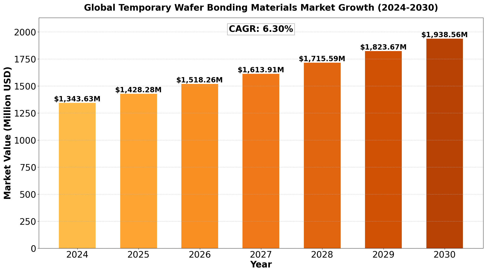
The Global Temporary Wafer Bonding Materials Market size was estimated at USD 1264 million in 2023 and is projected to reach USD 1938.56 million by 2030, exhibiting a CAGR of 6.30% during the forecast period.
North America Temporary Wafer Bonding Materials market size was USD 329.36 million in 2023, at a CAGR of 5.40% during the forecast period of 2024 through 2030.
Temporary Wafer Bonding Materials Key Market Trends :
- Increasing Demand for Advanced Packaging
- The rising need for compact, high-performance electronic devices is driving the adoption of wafer-level packaging techniques, boosting the Temporary Wafer Bonding Materials market.
- Growing Semiconductor Industry
- The continuous expansion of the semiconductor sector, fueled by AI, IoT, and 5G technologies, is significantly impacting the demand for wafer bonding materials.
- Shift Towards 3D IC Integration
- The adoption of 3D integrated circuits (ICs) to improve performance and reduce power consumption is increasing the necessity for high-quality bonding materials.
- Sustainability and Eco-friendly Materials
- Manufacturers are focusing on developing biodegradable and low-impact materials to meet global sustainability initiatives and regulatory requirements.
- Expansion of MEMS and Compound Semiconductors
- The rising demand for MEMS devices and compound semiconductors in automotive, consumer electronics, and healthcare is driving market growth.
Temporary Wafer Bonding Materials Market Regional Analysis :

-
North America:
Strong demand driven by EVs, 5G infrastructure, and renewable energy, with the U.S. leading the market.
-
Europe:
Growth fueled by automotive electrification, renewable energy, and strong regulatory support, with Germany as a key player.
-
Asia-Pacific:
Dominates the market due to large-scale manufacturing in China and Japan, with growing demand from EVs, 5G, and semiconductors.
-
South America:
Emerging market, driven by renewable energy and EV adoption, with Brazil leading growth.
-
Middle East & Africa:
Gradual growth, mainly due to investments in renewable energy and EV infrastructure, with Saudi Arabia and UAE as key contributors.
Temporary Wafer Bonding Materials Market Segmentation :
The research report includes specific segments by region (country), manufacturers, Type, and Application. Market segmentation creates subsets of a market based on product type, end-user or application, Geographic, and other factors. By understanding the market segments, the decision-maker can leverage this targeting in the product, sales, and marketing strategies. Market segments can power your product development cycles by informing how you create product offerings for different segments.
Key Company
- Brewer Science
- Samcien Semiconductor Materials
- Sekisui Chemical
- 3M
- HD MicroSystems (DuPont)
- Dow
- Henkel
- Nissan Chemical
- TOKYO OHKA KOGYO
- AI Technology
Market Segmentation (by Type)
- Thermoplastic Materials
- UV Curing Materials
- Composite Films
- Metallic Materials
- Others
Market Segmentation (by Application)
- Wafer-level Packaging
- MEMS
- Compound Semiconductor
- Others
Drivers
- Surging Demand for Consumer Electronics
- Increased adoption of smartphones, smart wearables, and IoT devices is fueling the demand for advanced semiconductor packaging solutions.
- Growth of the Automotive Semiconductor Market
- The rise of electric vehicles (EVs) and autonomous driving technology is boosting the need for high-performance semiconductor components.
- Advancements in 5G and AI Technologies
- Rapid development in AI-driven applications and 5G networks is driving the expansion of wafer bonding material usage.
Restraints
- High Cost of Temporary Wafer Bonding Materials
- The expensive nature of advanced bonding materials poses a challenge for small-scale manufacturers.
- Complex Manufacturing Processes
- The intricate bonding and debonding processes increase production complexity, requiring specialized expertise and equipment.
- Stringent Environmental Regulations
- Compliance with strict global environmental and safety regulations may hinder market expansion.
Opportunities
- Emerging Markets and Expanding Semiconductor Industry
- Growing semiconductor production in Asia-Pacific, particularly in China and India, presents lucrative opportunities.
- Development of Next-Generation Bonding Materials
- Innovations in bonding materials, such as hybrid and nanomaterial-based solutions, open new market prospects.
- Adoption of Advanced Packaging Technologies
- The rising demand for fan-out wafer-level packaging (FOWLP) and system-in-package (SiP) solutions is creating significant growth opportunities.
Challenges
- Supply Chain Disruptions
- Geopolitical issues, trade restrictions, and raw material shortages can impact supply chain stability.
- Limited Adoption in Small and Medium Enterprises
- High capital investment requirements prevent smaller manufacturers from entering the market.
- Technical Limitations in Bonding and Debonding
- Ensuring defect-free bonding and efficient debonding remains a significant challenge for manufacturers.
Key Benefits of This Market Research:
- Industry drivers, restraints, and opportunities covered in the study
- Neutral perspective on the market performance
- Recent industry trends and developments
- Competitive landscape & strategies of key players
- Potential & niche segments and regions exhibiting promising growth covered
- Historical, current, and projected market size, in terms of value
- In-depth analysis of the Temporary Wafer Bonding Materials Market
- Overview of the regional outlook of the Temporary Wafer Bonding Materials Market:
Key Reasons to Buy this Report:
- Access to date statistics compiled by our researchers. These provide you with historical and forecast data, which is analyzed to tell you why your market is set to change
- This enables you to anticipate market changes to remain ahead of your competitors
- You will be able to copy data from the Excel spreadsheet straight into your marketing plans, business presentations, or other strategic documents
- The concise analysis, clear graph, and table format will enable you to pinpoint the information you require quickly
- Provision of market value (USD Billion) data for each segment and sub-segment
- Indicates the region and segment that is expected to witness the fastest growth as well as to dominate the market
- Includes in-depth analysis of the market from various perspectives through Porters five forces analysis
- Provides insight into the market through Value Chain
- Market dynamics scenario, along with growth opportunities of the market in the years to come
- 6-month post-sales analyst support
Customization of the Report
In case of any queries or customization requirements, please connect with our sales team, who will ensure that your requirements are met.
FAQs
Q: What are the key driving factors and opportunities in the Temporary Wafer Bonding Materials market?
A: The market is driven by the rising demand for consumer electronics, advancements in semiconductor packaging, and the adoption of 5G and AI technologies. Opportunities include the expansion of the semiconductor industry and innovations in bonding materials.
Q: Which region is projected to have the largest market share?
A: Asia-Pacific is expected to dominate the market due to rapid semiconductor manufacturing growth, government investments, and high demand for electronic devices.
Q: Who are the top players in the global Temporary Wafer Bonding Materials market?
A: Leading companies include Brewer Science, 3M, Dow, Henkel, Sekisui Chemical, and TOKYO OHKA KOGYO.
Q: What are the latest technological advancements in the industry?
A: Recent advancements include the development of hybrid bonding materials, improvements in UV-curable adhesives, and innovations in eco-friendly wafer bonding solutions.
Q: What is the current size of the global Temporary Wafer Bonding Materials market?
A: The market was valued at USD 1264 million in 2023 and is projected to reach USD 1938.56 million by 2030, with a CAGR of 6.30%.

Get Sample Report PDF for Exclusive Insights
Report Sample Includes
- Table of Contents
- List of Tables & Figures
- Charts, Research Methodology, and more...


