Single Crystal Silicon Wafers (300Mm) Market Overview
Semiconductor silicon wafers are key component of integrated circuits such as those used to power computers, cell phones, and a wide variety of other devices. A silicon wafer consists of a thin slice of silicon which can be treated in various ways, depending on the type of electronics that is being used. Silicon has a very high quality semiconductor, making it ideal for the production of such circuits.
This report provides a deep insight into the global Single Crystal Silicon Wafers (300Mm) market covering all its essential aspects. This ranges from a macro overview of the market to micro details of the market size, competitive landscape, development trend, niche market, key market drivers and challenges, SWOT analysis, value chain analysis, etc.
The analysis helps the reader to shape the competition within the industries and strategies for the competitive environment to enhance the potential profit. Furthermore, it provides a simple framework for evaluating and accessing the position of the business organization. The report structure also focuses on the competitive landscape of the Global Single Crystal Silicon Wafers (300Mm) Market, this report introduces in detail the market share, market performance, product situation, operation situation, etc. of the main players, which helps the readers in the industry to identify the main competitors and deeply understand the competition pattern of the market.
In a word, this report is a must-read for industry players, investors, researchers, consultants, business strategists, and all those who have any kind of stake or are planning to foray into the Single Crystal Silicon Wafers (300Mm) market in any manner.
Single Crystal Silicon Wafers (300Mm) Market Analysis:
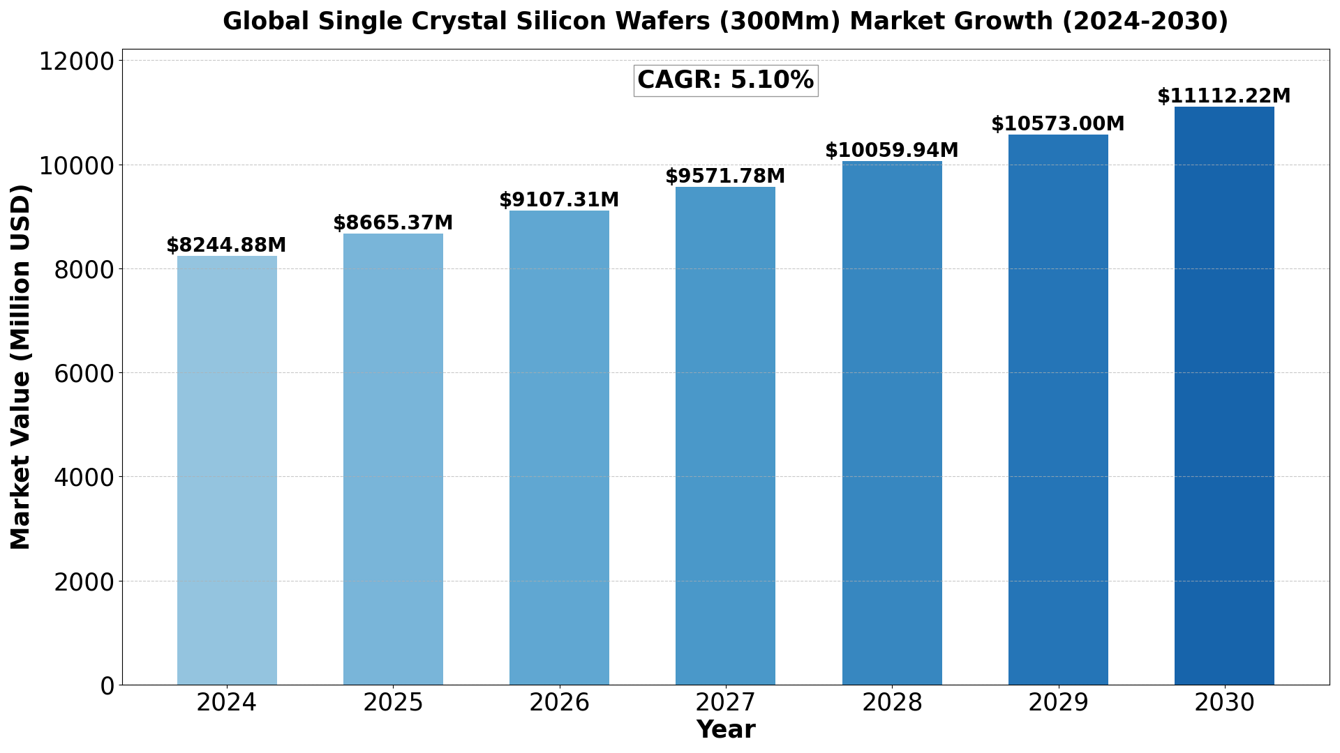
The global Single Crystal Silicon Wafers (300Mm) market size was estimated at USD 7844.80 million in 2023 and is projected to reach USD 11112.22 million by 2030, exhibiting a CAGR of 5.10% during the forecast period.
North America Single Crystal Silicon Wafers (300Mm) market size was USD 2044.13 million in 2023, at a CAGR of 4.37% during the forecast period of 2024 through 2030.
Access Your Free Sample Report Now
Single Crystal Silicon Wafers (300Mm) Key Market Trends :
1. Growth of Advanced Semiconductor Nodes
- 300mm wafers are primarily used in advanced semiconductor nodes (e.g., 5nm, 3nm, and below), where the miniaturization of transistors is key to improving chip performance and efficiency.
- As smaller process nodes become more critical for the development of high-performance computing (HPC), AI processors, and 5G chips, the demand for 300mm wafers continues to increase, particularly for cutting-edge applications.
2. Expansion of Semiconductor Manufacturing in AI, 5G, and Automotive
- The adoption of AI, 5G, and autonomous driving technologies is driving the need for more powerful and efficient semiconductors, often manufactured on 300mm silicon wafers.
- AI chips, 5G RF components, automotive sensors, and power semiconductors are among the key applications that benefit from the performance capabilities of 12-inch wafers, driving market growth.
3. Technological Advancements in Wafer Production and Yield Improvement
- Manufacturing technologies for 300mm wafers continue to advance, leading to improved yield rates and production efficiency.
- Enhanced chemical vapor deposition (CVD) and epitaxial growth techniques, as well as process optimization in wafer production, are helping semiconductor manufacturers produce higher-quality wafers at scale, ensuring reliable performance for next-generation devices.
4. Increasing Demand for Power Devices and IoT
- The IoT (Internet of Things) and automotive sectors are increasingly relying on power semiconductors and sensors that require high-performing chips, which are often made using 300mm silicon wafers.
- The shift towards electric vehicles (EVs) and smart grids is driving the demand for power management ICs and power semiconductors, which are frequently fabricated on 300mm wafers due to the need for high performance, energy efficiency, and low cost.
5. Investments in New Fab Facilities and Capacity Expansion
- Semiconductor foundries are continuing to invest heavily in new fabs and capacity expansion to meet the increasing demand for 300mm wafer production.
- The major players in the semiconductor foundry space, such as TSMC, Samsung, and Intel, are ramping up production capabilities for 12-inch wafers to ensure they can handle the increasing demand for cutting-edge chips used in high-growth areas like AI, 5G, and automotive electronics.
Single Crystal Silicon Wafers (300Mm) Market Regional Analysis :
1. North America (USA, Canada, Mexico)
- USA: The largest market in the region due to advanced infrastructure, high disposable income, and technological advancements. Key industries include technology, healthcare, and manufacturing.
- Canada: Strong market potential driven by resource exports, a stable economy, and government initiatives supporting innovation.
- Mexico: A growing economy with strengths in automotive manufacturing, agriculture, and tourism, benefitting from trade agreements like the USMCA.
2. Europe (Germany, UK, France, Russia, Italy, Rest of Europe)
- Germany: The region’s industrial powerhouse with a focus on engineering, automotive, and machinery.
- UK: A hub for financial services, fintech, and pharmaceuticals, though Brexit has altered trade patterns.
- France: Strong in luxury goods, agriculture, and aerospace with significant innovation in renewable energy.
- Russia: Resource-driven economy with strengths in oil, gas, and minerals but geopolitical tensions affect growth.
- Italy: Known for fashion, design, and manufacturing, especially in luxury segments.
- Rest of Europe: Includes smaller yet significant economies like Spain, Netherlands, and Switzerland with strengths in finance, agriculture, and manufacturing.
3. Asia-Pacific (China, Japan, South Korea, India, Southeast Asia, Rest of Asia-Pacific)
- China: The largest market in the region with a focus on technology, manufacturing, and e-commerce. Rapid urbanization and middle-class growth fuel consumption.
- Japan: Technological innovation, particularly in robotics and electronics, drives the economy.
- South Korea: Known for technology, especially in semiconductors and consumer electronics.
- India: Rapidly growing economy with strengths in IT services, agriculture, and pharmaceuticals.
- Southeast Asia: Key markets like Indonesia, Thailand, and Vietnam show growth in manufacturing and tourism.
- Rest of Asia-Pacific: Emerging markets with growing investment in infrastructure and services.
4. South America (Brazil, Argentina, Colombia, Rest of South America)
- Brazil: Largest economy in the region, driven by agriculture, mining, and energy.
- Argentina: Known for agriculture exports and natural resources but faces economic instability.
- Colombia: Growing economy with strengths in oil, coffee, and flowers.
- Rest of South America: Includes Chile and Peru, which have strong mining sectors.
5. The Middle East and Africa (Saudi Arabia, UAE, Egypt, Nigeria, South Africa, Rest of MEA)
- Saudi Arabia: Oil-driven economy undergoing diversification with Vision 2030 initiatives.
- UAE: Financial hub with strengths in tourism, real estate, and trade.
- Egypt: Growing infrastructure development and tourism.
- Nigeria: Largest economy in Africa with strengths in oil and agriculture.
- South Africa: Industrialized economy with strengths in mining and finance.
- Rest of MEA: Includes smaller yet resource-rich markets like Qatar and Kenya with growing infrastructure investments.
Single Crystal Silicon Wafers (300Mm) Market Segmentation :
The research report includes specific segments by region (country), manufacturers, Type, and Application. Market segmentation creates subsets of a market based on product type, end-user or application, Geographic, and other factors. By understanding the market segments, the decision-maker can leverage this targeting in the product, sales, and marketing strategies. Market segments can power your product development cycles by informing how you create product offerings for different segments.
Market Segmentation (by Type)
- 300mm Epitaxial Wafer
- 300mm Polished Wafer
- 300mm Annealed Wafer
Market Segmentation (by Application)
- Memory
- Logic/MPU
Single Crystal Silicon Wafers (300Mm) Market Competitive landscape :
- S.E.H
- Sumco
- Global Wafers
- Siltronic
- SK Siltron
- NSIG
- Zhonghuan
Drivers
- Advancements in Semiconductor Technology
The demand for high-performance and miniaturized semiconductors is increasing across multiple industries, including consumer electronics, automotive, telecommunications, and more. 300mm single crystal silicon wafers are a core component in the production of advanced semiconductor chips due to their ability to produce high-density, smaller, and more efficient transistors. This trend is significantly driving the growth of the 300mm silicon wafer market. - Growing Demand for Consumer Electronics
The global demand for smartphones, laptops, wearables, and other consumer electronics is a major driver for the 300mm silicon wafer market. As these devices require high-performance chips, the need for larger wafers, such as 300mm, has increased. These wafers enable the production of advanced integrated circuits (ICs) that power modern electronics, leading to more widespread adoption of 300mm wafers in mass production. - Increased Adoption of Electric Vehicles (EVs)
The growth of the electric vehicle market has created new opportunities for semiconductor manufacturers. EVs rely heavily on advanced semiconductor devices for various applications such as power management, infotainment, battery management systems (BMS), and autonomous driving technologies. These applications require high-performance semiconductors, often manufactured on 300mm single crystal silicon wafers, driving demand for these wafers in the automotive sector. - Transition to 5G and IoT Networks
The global rollout of 5G networks and the expansion of the Internet of Things (IoT) are increasing the need for advanced chips that require 300mm single crystal silicon wafers. 5G technologies, in particular, require high-performance and energy-efficient semiconductors, which are often manufactured using 300mm wafers. This is significantly contributing to the growth of the market as demand for next-generation networking and communication devices surges. - Economies of Scale in Semiconductor Production
The adoption of 300mm wafers allows semiconductor manufacturers to produce more chips per wafer compared to smaller wafers like 200mm, improving yields and reducing the cost per chip. This cost-efficiency is one of the primary drivers of the increased use of 300mm wafers, particularly in high-volume manufacturing environments such as those in the consumer electronics and automotive industries.
Restraints
- High Initial Capital Investment
Manufacturing 300mm wafers requires advanced semiconductor fabrication equipment, which can be extremely costly. The initial capital investment for setting up 300mm wafer production lines is significant, which can be a barrier for smaller manufacturers or new entrants in the market. Additionally, the infrastructure and cleanroom facilities required for 300mm wafer production are costly to maintain, which could limit the market’s growth. - Supply Chain and Material Constraints
The production of 300mm single crystal silicon wafers relies on a steady supply of high-quality raw materials. Shortages in materials such as high-purity silicon can lead to supply chain disruptions, which can negatively affect the availability and pricing of 300mm wafers. Additionally, fluctuations in material costs may put pressure on wafer manufacturers, affecting their ability to meet demand efficiently. - Technological Complexity and Process Challenges
The process of growing and preparing single crystal silicon wafers, especially 300mm wafers, is technologically complex. Ensuring consistent wafer quality with minimal defects requires highly specialized processes and expertise. The increasing complexity of semiconductor devices, with smaller nodes and higher transistor density, presents challenges in terms of maintaining wafer quality and production yield. - Competition from Alternative Wafer Technologies
While 300mm silicon wafers are widely used, there is growing interest in alternative wafer technologies, such as gallium nitride (GaN) and silicon carbide (SiC), particularly for high-power applications. These alternative materials offer advantages in terms of efficiency and performance, which could limit the demand for traditional silicon wafers in certain markets, particularly in power electronics and automotive sectors.
Opportunities
- Growth in Semiconductor Demand for AI and Machine Learning
Artificial intelligence (AI) and machine learning (ML) applications are driving the need for more powerful and efficient semiconductor chips. These applications require processors with advanced capabilities, which are often manufactured using 300mm single crystal silicon wafers. The rising demand for AI and ML systems, especially in data centers, edge computing, and autonomous systems, presents a significant opportunity for the 300mm wafer market. - Expansion in Emerging Markets
The demand for consumer electronics, automotive devices, and industrial equipment is growing rapidly in emerging markets such as China, India, and Southeast Asia. As these regions continue to industrialize and adopt advanced technologies, the need for semiconductors produced on 300mm wafers is expected to rise. Manufacturers expanding their capacity in these regions can tap into this growing market and increase their share of the global wafer production. - Development of Advanced Wafer Processing Technologies
Innovations in wafer processing technologies, such as improved etching, deposition, and cleaning techniques, can improve the quality and yield of 300mm wafers. Additionally, advancements in wafer thinning and packaging technologies could enable 300mm wafers to be used in more diverse applications, such as MEMS (Micro-Electro-Mechanical Systems) and power semiconductors, thus broadening their market potential. - Demand for High-Efficiency Power Devices
With the increasing focus on renewable energy, energy-efficient systems, and power electronics, 300mm wafers are increasingly being used to manufacture power semiconductor devices such as power transistors and diodes. The shift towards energy-efficient technologies presents a key opportunity for 300mm wafer manufacturers, particularly in the context of electric vehicles, energy storage systems, and industrial automation. - Technological Advancements in Wafer Scaling
The continued trend towards smaller semiconductor nodes and more advanced technologies, including the adoption of extreme ultraviolet (EUV) lithography, is driving demand for high-quality wafers. Manufacturers who can successfully scale the production of 300mm wafers for smaller nodes and advanced processes will find substantial growth opportunities in the development of next-generation semiconductor devices.
Challenges
- Intense Competition from Larger Wafer Sizes (450mm)
While 300mm wafers are the standard in many semiconductor applications, there is ongoing research into larger wafer sizes, particularly the potential shift toward 450mm wafers. Larger wafers offer increased productivity and cost-effectiveness, which could reduce the long-term demand for 300mm wafers. This shift could present a challenge for the market as manufacturers move toward larger wafer technologies. - Environmental and Regulatory Compliance
The semiconductor industry is increasingly facing pressure to reduce its environmental footprint, including energy consumption, waste generation, and the use of hazardous materials. Meeting environmental regulations and sustainability standards while maintaining cost-effectiveness in 300mm wafer production could pose challenges to wafer manufacturers. Adapting to these regulations may increase costs and complexity in the production process. - Yield and Quality Control Issues
As the semiconductor industry pushes for smaller and more advanced nodes, ensuring consistent quality and high yields for 300mm wafers becomes increasingly challenging. Defects in the wafer or variations in the crystalline structure can lead to a lower yield of usable chips, which directly impacts the profitability of wafer manufacturers. Maintaining high-quality standards amidst these challenges is a key concern for the industry.
Key Benefits of This Market Research:
- Industry drivers, restraints, and opportunities covered in the study
- Neutral perspective on the market performance
- Recent industry trends and developments
- Competitive landscape & strategies of key players
- Potential & niche segments and regions exhibiting promising growth covered
- Historical, current, and projected market size, in terms of value
- In-depth analysis of the Semiconductor Lens Market
- Overview of the regional outlook of the Semiconductor Lens Market:
Key Reasons to Buy this Report:
- Access to date statistics compiled by our researchers. These provide you with historical and forecast data, which is analyzed to tell you why your market is set to change
- This enables you to anticipate market changes to remain ahead of your competitors
- You will be able to copy data from the Excel spreadsheet straight into your marketing plans, business presentations, or other strategic documents
- The concise analysis, clear graph, and table format will enable you to pinpoint the information you require quickly
- Provision of market value (USD Billion) data for each segment and sub-segment
- Indicates the region and segment that is expected to witness the fastest growth as well as to dominate the market
- Analysis by geography highlighting the consumption of the product/service in the region as well as indicating the factors that are affecting the market within each region
- Competitive landscape which incorporates the market ranking of the major players, along with new service/product launches, partnerships, business expansions, and acquisitions in the past five years of companies profiled
- Extensive company profiles comprising of company overview, company insights, product benchmarking, and SWOT analysis for the major market players
- The current as well as the future market outlook of the industry concerning recent developments which involve growth opportunities and drivers as well as challenges and restraints of both emerging as well as developed regions
- Includes in-depth analysis of the market from various perspectives through Porters five forces analysis
- Provides insight into the market through Value Chain
- Market dynamics scenario, along with growth opportunities of the market in the years to come
- 6-month post-sales analyst support
In case of any queries or customization requirements, please connect with our sales team, who will ensure that your requirements are met.
FAQs
Q1. What is the Single Crystal Silicon Wafers (300mm) Market?
A1. The Single Crystal Silicon Wafers (300mm) Market involves the production and supply of high-quality silicon wafers used in the fabrication of semiconductors, where 300mm wafers are preferred for advanced semiconductor manufacturing, offering higher yields and cost efficiency.
Q2. What is the current market size and forecast for the Global Single Crystal Silicon Wafers (300mm) Market?
A2. The market size was estimated at USD 7844.80 million in 2023 and is projected to reach USD 11112.22 million by 2030, growing at a CAGR of 5.10% during the forecast period.
Q3. What are the key growth drivers in the Global Single Crystal Silicon Wafers (300mm) Market?
A3. Key growth drivers include the increasing demand for high-performance semiconductors, advancements in semiconductor manufacturing technologies, and the growing need for larger wafers in the production of integrated circuits for applications in consumer electronics, automotive, and telecommunications.
Q4. Which regions dominate the Global Single Crystal Silicon Wafers (300mm) Market?
A4. Asia-Pacific dominates the market due to its extensive semiconductor manufacturing industry, with major producers located in countries like Taiwan, South Korea, and China. North America and Europe also play significant roles in the market.
Q5. What are the emerging trends in the Global Single Crystal Silicon Wafers (300mm) Market?
A5. Emerging trends include innovations in wafer manufacturing for enhanced efficiency, the increasing shift towards 300mm wafers in advanced semiconductor processes, and the rise of AI, 5G, and electric vehicle technologies driving the demand for high-performance semiconductors.

Get Sample Report PDF for Exclusive Insights
Report Sample Includes
- Table of Contents
- List of Tables & Figures
- Charts, Research Methodology, and more...