Semiconductor Packaging Material Market Overview
Semiconductor packaging materials play an important role in protecting IC chips from the surrounding environment, ensuring electrical connection for chip mount on printed wiring boards. Demand for high-speed, high-integration and low power consumption of ICs accompanying the rapid progress of electronics technology such as AI, Cloud computing, Intelligentization of automobiles, and due to the miniaturization and thinning of electronic devices typified by smart phone and wearable devices, semiconductor packages are required further high density, multilayer, low-profile.
This report provides a deep insight into the global Semiconductor Packaging Material market covering all its essential aspects. This ranges from a macro overview of the market to micro details of the market size, competitive landscape, development trend, niche market, key market drivers and challenges, SWOT analysis, value chain analysis, etc.
The analysis helps the reader to shape the competition within the industries and strategies for the competitive environment to enhance the potential profit. Furthermore, it provides a simple framework for evaluating and accessing the position of the business organization. The report structure also focuses on the competitive landscape of the Global Semiconductor Packaging Material Market, this report introduces in detail the market share, market performance, product situation, operation situation, etc. of the main players, which helps the readers in the industry to identify the main competitors and deeply understand the competition pattern of the market.
In a word, this report is a must-read for industry players, investors, researchers, consultants, business strategists, and all those who have any kind of stake or are planning to foray into the Semiconductor Packaging Material market in any manner.
Semiconductor Packaging Material Market Analysis:
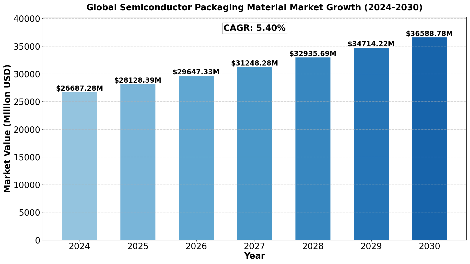
The Global Semiconductor Packaging Material Market size was estimated at USD 25320 million in 2023 and is projected to reach USD 36588.78 million by 2030, exhibiting a CAGR of 5.40% during the forecast period.
North America Semiconductor Packaging Material market size was USD 6597.67 million in 2023, at a CAGR of 4.63% during the forecast period of 2024 through 2030.
Access Your Free Sample Report Now
Semiconductor Packaging Material Key Market Trends :
1. Growth of Advanced Packaging Technologies
- The rise of chiplet-based designs, 3D stacking, and fan-out wafer-level packaging (FOWLP) is driving demand for specialized packaging materials that enhance performance and durability.
- Materials like underfill encapsulants, mold compounds, and organic substrates are critical to achieving high integration and miniaturization in modern semiconductor devices.
2. Increased Demand from Automotive and 5G Applications
- The adoption of semiconductors in electric vehicles (EVs), autonomous driving systems, and 5G infrastructure is propelling the need for packaging materials capable of withstanding harsh environments and high frequencies.
- Thermal interface materials (TIMs) and high-reliability mold compounds are seeing increased adoption in these sectors.
3. Focus on Lightweight and High-Performance Materials
- The push for smaller, lighter, and more powerful electronic devices is leading to the development of low-density packaging materials that offer superior thermal and electrical properties.
- Materials like polyimide films, liquid crystal polymers (LCPs), and epoxy molding compounds are being widely adopted for their performance benefits.
4. Sustainability and Eco-Friendly Packaging Materials
- Manufacturers are prioritizing environmentally friendly materials, driven by global regulations and the industry’s focus on sustainability.
- This includes innovations in biodegradable mold compounds, recyclable substrates, and low-VOC (volatile organic compound) adhesives.
5. Regional Investments in Semiconductor Manufacturing
- Increasing investments in semiconductor manufacturing facilities, particularly in regions like Asia-Pacific, North America, and Europe, are fueling demand for packaging materials.
- Countries like China, Taiwan, and South Korea dominate the market, with heavy investments in packaging material innovation to support domestic semiconductor production.
Semiconductor Packaging Material Market Regional Analysis :
1. North America (USA, Canada, Mexico)
- USA: The largest market in the region due to advanced infrastructure, high disposable income, and technological advancements. Key industries include technology, healthcare, and manufacturing.
- Canada: Strong market potential driven by resource exports, a stable economy, and government initiatives supporting innovation.
- Mexico: A growing economy with strengths in automotive manufacturing, agriculture, and tourism, benefitting from trade agreements like the USMCA.
2. Europe (Germany, UK, France, Russia, Italy, Rest of Europe)
- Germany: The region’s industrial powerhouse with a focus on engineering, automotive, and machinery.
- UK: A hub for financial services, fintech, and pharmaceuticals, though Brexit has altered trade patterns.
- France: Strong in luxury goods, agriculture, and aerospace with significant innovation in renewable energy.
- Russia: Resource-driven economy with strengths in oil, gas, and minerals but geopolitical tensions affect growth.
- Italy: Known for fashion, design, and manufacturing, especially in luxury segments.
- Rest of Europe: Includes smaller yet significant economies like Spain, Netherlands, and Switzerland with strengths in finance, agriculture, and manufacturing.
3. Asia-Pacific (China, Japan, South Korea, India, Southeast Asia, Rest of Asia-Pacific)
- China: The largest market in the region with a focus on technology, manufacturing, and e-commerce. Rapid urbanization and middle-class growth fuel consumption.
- Japan: Technological innovation, particularly in robotics and electronics, drives the economy.
- South Korea: Known for technology, especially in semiconductors and consumer electronics.
- India: Rapidly growing economy with strengths in IT services, agriculture, and pharmaceuticals.
- Southeast Asia: Key markets like Indonesia, Thailand, and Vietnam show growth in manufacturing and tourism.
- Rest of Asia-Pacific: Emerging markets with growing investment in infrastructure and services.
4. South America (Brazil, Argentina, Colombia, Rest of South America)
- Brazil: Largest economy in the region, driven by agriculture, mining, and energy.
- Argentina: Known for agriculture exports and natural resources but faces economic instability.
- Colombia: Growing economy with strengths in oil, coffee, and flowers.
- Rest of South America: Includes Chile and Peru, which have strong mining sectors.
5. The Middle East and Africa (Saudi Arabia, UAE, Egypt, Nigeria, South Africa, Rest of MEA)
- Saudi Arabia: Oil-driven economy undergoing diversification with Vision 2030 initiatives.
- UAE: Financial hub with strengths in tourism, real estate, and trade.
- Egypt: Growing infrastructure development and tourism.
- Nigeria: Largest economy in Africa with strengths in oil and agriculture.
- South Africa: Industrialized economy with strengths in mining and finance.
- Rest of MEA: Includes smaller yet resource-rich markets like Qatar and Kenya with growing infrastructure investments.
Semiconductor Packaging Material Market Segmentation :
The research report includes specific segments by region (country), manufacturers, Type, and Application. Market segmentation creates subsets of a market based on product type, end-user or application, Geographic, and other factors. By understanding the market segments, the decision-maker can leverage this targeting in the product, sales, and marketing strategies. Market segments can power your product development cycles by informing how you create product offerings for different segments.
Market Segmentation (by Type)
- IC Substrates
- Leadframe
- Encapsulant
- Ceramic Packages
- Underfill
- Tape
- Others
Market Segmentation (by Application)
- Traditional Packaging
- Advanced Materials
Semiconductor Packaging Material Market Competitive landscape :
- Unimicron
- Ibiden
- Nan Ya PCB
- Shinko Electric Industries
- Kinsus Interconnect Technology
- AT&S
- Samsung Electro-Mechanics
- Kyocera
- Toppan
- Zhen Ding Technology
- Daeduck Electronics
- Zhuhai Access Semiconductor
- LG InnoTek
- Shennan Circuit
- Shenzhen Fastprint Circuit Tech
- Mitsui High-tec
- Henkel
- Chang Wah Technology
- Advanced Assembly Materials International
- HAESUNG DS
- Fusheng Electronics
- Enomoto
- Kangqiang
- POSSEHL
- JIH LIN TECHNOLOGY
- Hualong
- Dynacraft Industries
- QPL Limited
- WUXI HUAJING LEADFRAME
- HUAYANG ELECTRONIC
- DNP
- Xiamen Jsun Precision Technology
- Sumitomo Bakelite
- Showa Denko
- Chang Chun Group
- Hysol Huawei Electronics
- Panasonic
- KCC
- Eternal Materials
- Jiangsu Zhongpeng New Material
- Shin-Etsu Chemical
- HHCK
- Scienchem
- Beijing Sino-tech Electronic Material
- Hysolem
Download Your Complimentary Sample Report
Drivers
- Growing Demand for Miniaturized and High-Performance Devices
With the increasing demand for compact and high-performance electronic devices like smartphones, wearables, and laptops, the need for advanced semiconductor packaging materials has surged. These materials ensure functionality, reliability, and thermal management in compact designs. - Advancements in Semiconductor Packaging Technologies
Innovations in packaging technologies, such as 3D packaging, fan-out wafer-level packaging (FOWLP), and system-in-package (SiP), are driving demand for advanced materials like substrate-based laminates, molding compounds, and encapsulation resins. - Proliferation of IoT and 5G Technologies
The rapid deployment of IoT devices and 5G networks has increased the demand for semiconductors requiring high-quality packaging materials to ensure performance, durability, and signal integrity in connected devices. - Growth in Automotive Electronics and EVs
The rise of electric vehicles (EVs) and advanced driver-assistance systems (ADAS) has amplified the need for semiconductor packaging materials. Automotive applications require robust packaging materials that can withstand extreme temperatures and vibrations. - Increased Focus on Chip Reliability and Thermal Management
As semiconductor chips become more powerful and compact, managing heat and ensuring structural integrity have become critical. High-performance packaging materials like thermal interface materials (TIMs) and solder balls are essential to maintain performance.
Restraints
- High Costs of Advanced Packaging Materials
Advanced packaging materials such as substrates for FOWLP, high-performance laminates, and advanced adhesives are costly. The high prices may hinder adoption, particularly for manufacturers with tight budgets. - Complex Manufacturing Processes
The production of advanced semiconductor packaging materials involves precise engineering and stringent quality control, leading to increased production costs and extended development times. - Environmental and Regulatory Challenges
The use of certain chemicals and materials in semiconductor packaging, such as lead-based solder, is facing increasing scrutiny due to environmental concerns. Stricter regulations on hazardous materials pose challenges for manufacturers. - Supply Chain Disruptions
Global semiconductor supply chain disruptions, exacerbated by geopolitical tensions and natural disasters, have impacted the availability and cost of raw materials, affecting the production of packaging materials.
Opportunities
- Emergence of Sustainable and Eco-Friendly Materials
The shift toward environmentally friendly practices has created opportunities for the development of sustainable packaging materials, such as biodegradable resins and lead-free solder. - Expansion in Emerging Markets
Countries like China, India, and Vietnam are witnessing significant investments in semiconductor manufacturing. These regions offer immense growth potential for packaging material suppliers aiming to expand their footprint. - Growth of Advanced Computing Applications
The rise of AI, machine learning, and data centers has created demand for high-performance semiconductors. Advanced packaging materials that can support higher power densities and thermal management are in high demand. - Innovations in Flexible and Wearable Electronics
The increasing adoption of flexible and wearable electronics has opened opportunities for materials such as flexible substrates and encapsulants, which are crucial for non-traditional packaging solutions. - Focus on Heterogeneous Integration
The industry trend toward integrating multiple functionalities on a single chip through technologies like SiP and 2.5D/3D integration presents an opportunity for specialized packaging materials designed for complex structures.
Challenges
- Rapid Technological Evolution
The semiconductor packaging market evolves rapidly, with constant innovation in technologies and materials. Staying ahead of trends requires continuous R&D investment, which can be resource-intensive. - Limited Availability of Raw Materials
Some raw materials, such as copper foils and high-purity silicon, are experiencing supply shortages due to growing global demand, leading to delays and cost increases. - High Energy and Resource Consumption in Manufacturing
The production of semiconductor packaging materials often involves high energy consumption and resource-intensive processes, making it challenging for manufacturers to meet sustainability goals. - Intense Market Competition
The semiconductor packaging material market is highly competitive, with several global and regional players offering similar products. This competition exerts pressure on pricing and profit margins.
Key Benefits of This Market Research:
- Industry drivers, restraints, and opportunities covered in the study
- Neutral perspective on the market performance
- Recent industry trends and developments
- Competitive landscape & strategies of key players
- Potential & niche segments and regions exhibiting promising growth covered
- Historical, current, and projected market size, in terms of value
- In-depth analysis of the Semiconductor Lens Market
- Overview of the regional outlook of the Semiconductor Lens Market:
Key Reasons to Buy this Report:
- Access to date statistics compiled by our researchers. These provide you with historical and forecast data, which is analyzed to tell you why your market is set to change
- This enables you to anticipate market changes to remain ahead of your competitors
- You will be able to copy data from the Excel spreadsheet straight into your marketing plans, business presentations, or other strategic documents
- The concise analysis, clear graph, and table format will enable you to pinpoint the information you require quickly
- Provision of market value (USD Billion) data for each segment and sub-segment
- Indicates the region and segment that is expected to witness the fastest growth as well as to dominate the market
- Analysis by geography highlighting the consumption of the product/service in the region as well as indicating the factors that are affecting the market within each region
- Competitive landscape which incorporates the market ranking of the major players, along with new service/product launches, partnerships, business expansions, and acquisitions in the past five years of companies profiled
- Extensive company profiles comprising of company overview, company insights, product benchmarking, and SWOT analysis for the major market players
- The current as well as the future market outlook of the industry concerning recent developments which involve growth opportunities and drivers as well as challenges and restraints of both emerging as well as developed regions
- Includes in-depth analysis of the market from various perspectives through Porters five forces analysis
- Provides insight into the market through Value Chain
- Market dynamics scenario, along with growth opportunities of the market in the years to come
- 6-month post-sales analyst support
In case of any queries or customization requirements, please connect with our sales team, who will ensure that your requirements are met.
FAQs
Q1. What is the Semiconductor Packaging Material Market?
A1. The Semiconductor Packaging Material Market encompasses materials used in the packaging process of semiconductor devices, ensuring protection, performance, and reliability of electronic components.
Q2. What is the current market size and forecast for the Global Semiconductor Packaging Material Market?
A2. The market size was estimated at USD 25320 million in 2023 and is projected to reach USD 36588.78 million by 2030, growing at a CAGR of 5.40% during the forecast period.
Q3. What are the key growth drivers in the Global Semiconductor Packaging Material Market?
A3. Key drivers include the growing demand for advanced semiconductor devices, increasing adoption of 5G and IoT technologies, and innovations in packaging to support miniaturized and high-performance devices.
Q4. Which regions dominate the Global Semiconductor Packaging Material Market?
A4. Asia-Pacific dominates the market due to its strong semiconductor manufacturing base, followed by North America and Europe, which benefit from advancements in packaging technologies and increasing investments in semiconductor R&D.
Q5. What are the emerging trends in the Global Semiconductor Packaging Material Market?
A5. Emerging trends include the rise of eco-friendly packaging materials, the development of advanced materials for 3D and system-in-package (SiP) technologies, and increasing integration of automation in the packaging process.
Get Sample Report PDF for Exclusive Insights
Report Sample Includes
- Table of Contents
- List of Tables & Figures
- Charts, Research Methodology, and more...