Semiconductor Metrology and Inspection Market Overview
Semiconductor Metrology and Inspection are important for the management of the semiconductor manufacturing process. There are 400 to 600 steps in the overall manufacturing process of semiconductor wafers, which are undertaken in the course of one to two months. If any defects occur early on in the process, all the work undertaken in the subsequent time-consuming steps will be wasted. The main segment in the report includes mask inspection, film inspection, optical inspection, wafer defect inspection, macro defect inspection and image wafer inspection, etc.
The analysis helps the reader to shape the competition within the industries and strategies for the competitive environment to enhance the potential profit. Furthermore, it provides a simple framework for evaluating and accessing the position of the business organization. The report structure also focuses on the competitive landscape of the Global Semiconductor Metrology and Inspection Market, this report introduces in detail the market share, market performance, product situation, operation situation, etc. of the main players, which helps the readers in the industry to identify the main competitors and deeply understand the competition pattern of the market.
In a word, this report is a must-read for industry players, investors, researchers, consultants, business strategists, and all those who have any kind of stake or are planning to foray into the Semiconductor Metrology and Inspection market in any manner.
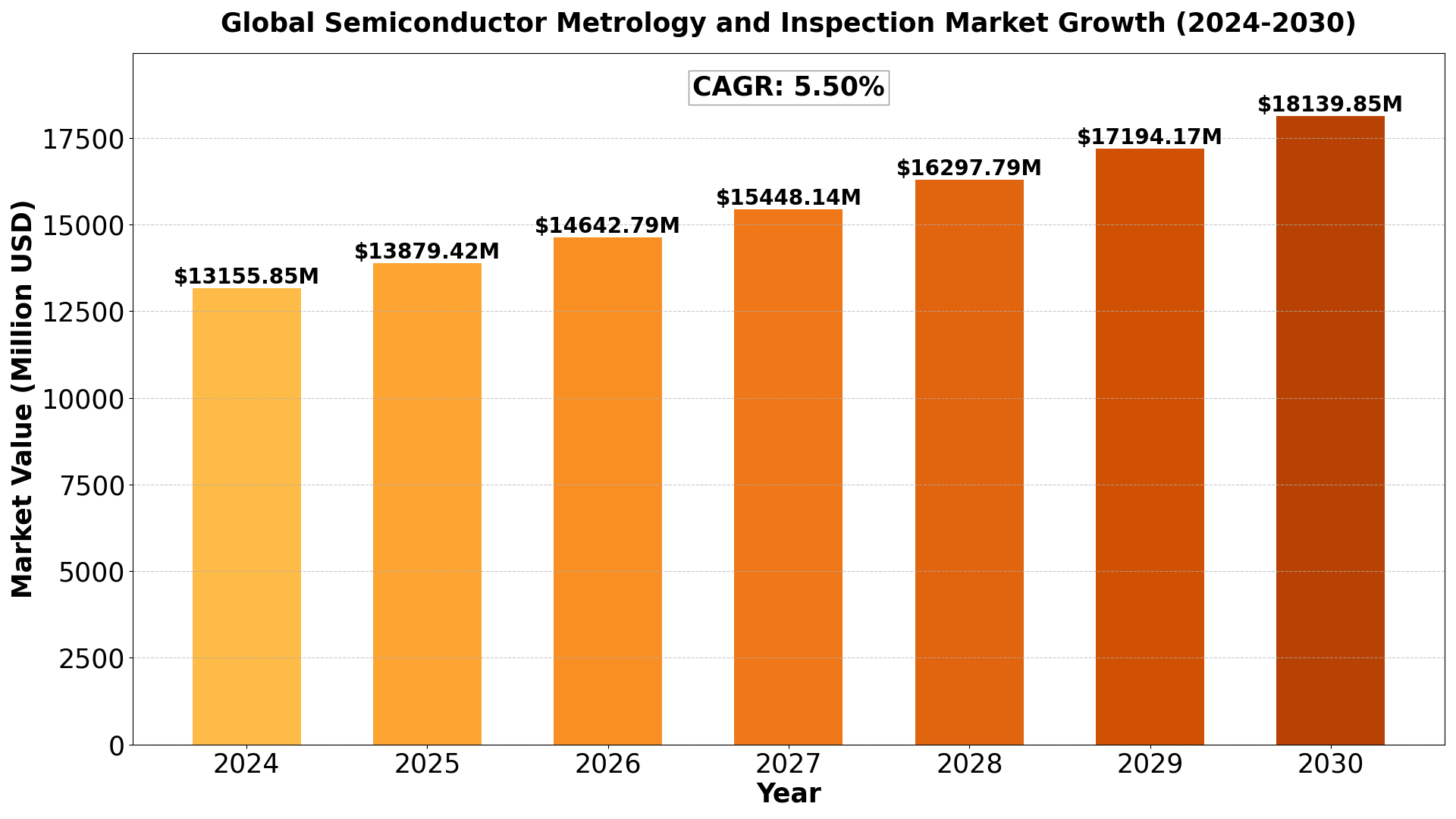
The Global Semiconductor Metrology and Inspection Market size was estimated at USD 12470 million in 2023 and is projected to reach USD 18139.85 million by 2030, exhibiting a CAGR of 5.50% during the forecast period.
North America Semiconductor Metrology and Inspection market size was USD 3249.33 million in 2023, at a CAGR of 4.71% during the forecast period of 2024 through 2030.
Access Your Free Sample Report Now
Semiconductor Metrology and Inspection Key Market Trends :
1. Demand for Advanced Node Metrology Solutions
- The shift toward smaller nodes (e.g., 5nm, 3nm, and beyond) in semiconductor manufacturing is driving demand for metrology and inspection tools capable of ultra-high precision.
- Atomic-level metrology techniques, such as CD-SEM (Critical Dimension Scanning Electron Microscopy) and optical overlay metrology, are becoming essential to ensure accuracy in patterning and etching processes.
2. Integration of Artificial Intelligence and Machine Learning
- AI and ML technologies are being integrated into metrology and inspection equipment to enhance defect detection, classification, and predictive analytics.
- These capabilities help manufacturers identify trends, optimize processes, and improve yield rates by automating decision-making and reducing human error.
3. Increased Adoption of In-Line Metrology
- Manufacturers are shifting from traditional offline to in-line metrology solutions to enable real-time monitoring and control during semiconductor production.
- In-line metrology allows for quicker identification of process deviations, improving overall efficiency and reducing the time required to bring products to market.
4. Focus on EUV Lithography Inspection
- The adoption of extreme ultraviolet (EUV) lithography for advanced semiconductor nodes is creating demand for specialized inspection tools.
- EUV-specific metrology systems, such as actinic inspection and EUV mask defect detection, are critical for ensuring the accuracy and reliability of next-generation chips.
5. Growth in Advanced Packaging Inspection
- The rise of heterogeneous integration and advanced packaging techniques, such as chiplets, 2.5D/3D ICs, and fan-out wafer-level packaging (FOWLP), is driving demand for inspection solutions tailored for these processes.
- Metrology tools for bump inspection, warpage measurement, and void detection are becoming more sophisticated to address the complexities of advanced packaging.
Semiconductor Metrology and Inspection Market Regional Analysis :
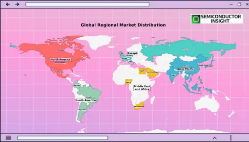
1. North America (USA, Canada, Mexico)
- USA: The largest market in the region due to advanced infrastructure, high disposable income, and technological advancements. Key industries include technology, healthcare, and manufacturing.
- Canada: Strong market potential driven by resource exports, a stable economy, and government initiatives supporting innovation.
- Mexico: A growing economy with strengths in automotive manufacturing, agriculture, and tourism, benefitting from trade agreements like the USMCA.
2. Europe (Germany, UK, France, Russia, Italy, Rest of Europe)
- Germany: The region’s industrial powerhouse with a focus on engineering, automotive, and machinery.
- UK: A hub for financial services, fintech, and pharmaceuticals, though Brexit has altered trade patterns.
- France: Strong in luxury goods, agriculture, and aerospace with significant innovation in renewable energy.
- Russia: Resource-driven economy with strengths in oil, gas, and minerals but geopolitical tensions affect growth.
- Italy: Known for fashion, design, and manufacturing, especially in luxury segments.
- Rest of Europe: Includes smaller yet significant economies like Spain, Netherlands, and Switzerland with strengths in finance, agriculture, and manufacturing.
3. Asia-Pacific (China, Japan, South Korea, India, Southeast Asia, Rest of Asia-Pacific)
- China: The largest market in the region with a focus on technology, manufacturing, and e-commerce. Rapid urbanization and middle-class growth fuel consumption.
- Japan: Technological innovation, particularly in robotics and electronics, drives the economy.
- South Korea: Known for technology, especially in semiconductors and consumer electronics.
- India: Rapidly growing economy with strengths in IT services, agriculture, and pharmaceuticals.
- Southeast Asia: Key markets like Indonesia, Thailand, and Vietnam show growth in manufacturing and tourism.
- Rest of Asia-Pacific: Emerging markets with growing investment in infrastructure and services.
4. South America (Brazil, Argentina, Colombia, Rest of South America)
- Brazil: Largest economy in the region, driven by agriculture, mining, and energy.
- Argentina: Known for agriculture exports and natural resources but faces economic instability.
- Colombia: Growing economy with strengths in oil, coffee, and flowers.
- Rest of South America: Includes Chile and Peru, which have strong mining sectors.
5. The Middle East and Africa (Saudi Arabia, UAE, Egypt, Nigeria, South Africa, Rest of MEA)
- Saudi Arabia: Oil-driven economy undergoing diversification with Vision 2030 initiatives.
- UAE: Financial hub with strengths in tourism, real estate, and trade.
- Egypt: Growing infrastructure development and tourism.
- Nigeria: Largest economy in Africa with strengths in oil and agriculture.
- South Africa: Industrialized economy with strengths in mining and finance.
- Rest of MEA: Includes smaller yet resource-rich markets like Qatar and Kenya with growing infrastructure investments.
Semiconductor Metrology and Inspection Market Segmentation :
The research report includes specific segments by region (country), manufacturers, Type, and Application. Market segmentation creates subsets of a market based on product type, end-user or application, Geographic, and other factors. By understanding the market segments, the decision-maker can leverage this targeting in the product, sales, and marketing strategies. Market segments can power your product development cycles by informing how you create product offerings for different segments.
Market Segmentation (by Type)
- Defect Inspection Equipment
- Metrology Equipment
Market Segmentation (by Application)
- Wafer
- Mask/Film
- Others
Semiconductor Metrology and Inspection Market Competitive landscape :
- KLA Corporation
- Applied Materials
- Hitachi High-Technologies
- ASML
- Onto Innovation
- Lasertec
- SCREEN Semiconductor Solutions
- ZEISS
- Camtek
- Toray Engineering
- Muetec
- Unity Semiconductor SAS
- Microtronic
- RSIC
- Nova
Download Your Complimentary Sample Report
Drivers
- Growing Demand for Semiconductor Devices
The rapid adoption of advanced technologies like AI, IoT, 5G, and autonomous vehicles is fueling the demand for semiconductors. This drives the need for precise metrology and inspection solutions to ensure high-quality production. - Technological Advancements in Semiconductor Manufacturing
Shrinking node sizes and the complexity of integrated circuits (ICs) require innovative metrology tools for accurate measurement and defect detection, driving market growth. - Rising Investment in Semiconductor Fabrication Facilities
Governments and private players are increasing investments in fabs to enhance semiconductor production capacity, thereby boosting demand for metrology and inspection equipment.
Restraints
- High Cost of Advanced Equipment
The cost of acquiring and maintaining cutting-edge metrology and inspection tools is significant, making it a barrier for smaller semiconductor manufacturers. - Complexity in Inspecting Smaller Nodes
As semiconductor nodes continue to shrink (e.g., below 5nm), inspection and measurement become increasingly challenging, slowing the pace of adoption in some cases.
Opportunities
- Emergence of EUV Lithography
Extreme Ultraviolet (EUV) lithography is gaining traction for advanced chip manufacturing. This creates opportunities for specialized metrology and inspection solutions tailored for EUV processes. - Demand from Emerging Markets
The growth of semiconductor manufacturing in countries like China, South Korea, and Taiwan presents untapped opportunities for metrology and inspection solution providers. - Adoption of AI and Machine Learning
Integrating AI and ML in metrology and inspection systems is enabling real-time analysis and defect prediction, enhancing production efficiency.
Challenges
- Keeping Pace with Rapid Technological Changes
The continuous evolution of semiconductor manufacturing technologies poses a challenge for metrology and inspection tool developers to stay ahead. - Global Semiconductor Supply Chain Disruptions
Issues such as geopolitical tensions and pandemic-related disruptions can impact the supply chain, affecting the adoption of metrology and inspection tools.
Key Benefits of This Market Research:
- Industry drivers, restraints, and opportunities covered in the study
- Neutral perspective on the market performance
- Recent industry trends and developments
- Competitive landscape & strategies of key players
- Potential & niche segments and regions exhibiting promising growth covered
- Historical, current, and projected market size, in terms of value
- In-depth analysis of the Semiconductor Metrology and Inspection Market
- Overview of the regional outlook of the Semiconductor Metrology and Inspection Market:
Key Reasons to Buy this Report:
- Access to date statistics compiled by our researchers. These provide you with historical and forecast data, which is analyzed to tell you why your market is set to change
- This enables you to anticipate market changes to remain ahead of your competitors
- You will be able to copy data from the Excel spreadsheet straight into your marketing plans, business presentations, or other strategic documents
- The concise analysis, clear graph, and table format will enable you to pinpoint the information you require quickly
- Provision of market value (USD Billion) data for each segment and sub-segment
- Indicates the region and segment that is expected to witness the fastest growth as well as to dominate the market
- Analysis by geography highlighting the consumption of the product/service in the region as well as indicating the factors that are affecting the market within each region
- Competitive landscape which incorporates the market ranking of the major players, along with new service/product launches, partnerships, business expansions, and acquisitions in the past five years of companies profiled
- Extensive company profiles comprising of company overview, company insights, product benchmarking, and SWOT analysis for the major market players
- The current as well as the future market outlook of the industry concerning recent developments which involve growth opportunities and drivers as well as challenges and restraints of both emerging as well as developed regions
- Includes in-depth analysis of the market from various perspectives through Porters five forces analysis
- Provides insight into the market through Value Chain
- Market dynamics scenario, along with growth opportunities of the market in the years to come
- 6-month post-sales analyst support
Customization of the Report
In case of any queries or customization requirements, please connect with our sales team, who will ensure that your requirements are met.
FAQs

Get Sample Report PDF for Exclusive Insights
Report Sample Includes
- Table of Contents
- List of Tables & Figures
- Charts, Research Methodology, and more...