
Key Statistics
Key Takeaways
- CTE above 5 ppm/°C is the leading source-defined type because the segment is aligned with packaging designs that need dimensional stability while still accommodating board- and die-level thermomechanical behavior; lower-CTE formulations remain strategically important where tighter silicon matching is required.
- Wafer-level packaging is the leading application, while panel-level packaging is the main scale-up opportunity because larger-format processing can improve package area utilization and manufacturing economics if glass handling, via yield and metallization uniformity are controlled.
- Asia Pacific is the largest market, supported by the concentration of substrate, OSAT, foundry and electronics manufacturing across Japan, Taiwan, South Korea and China. North America has an outsized technology role because U.S. advanced-packaging programs are pushing large package bodies for AI.
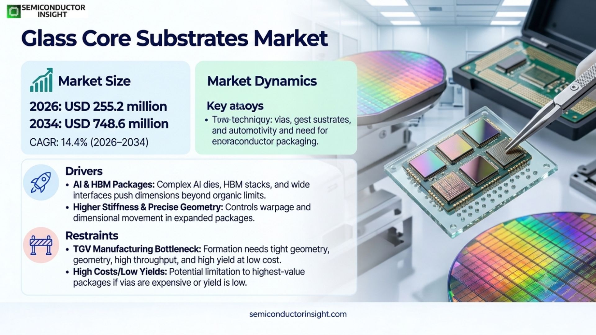
- The strongest demand driver is advanced packaging for AI and HPC. Glass offers stiffness, flatness, tunable CTE and low electrical loss that become more valuable as chiplet counts, package dimensions, HBM interfaces and high-speed signaling increase.
- The principal restraint is manufacturing maturity. Through-glass-via formation, metallization adhesion, brittle-material handling, panel flatness and package-level reliability must reach high-volume yield targets before glass can displace mature organic substrates beyond premium applications.
- The strategic opportunity is ecosystem integration. Material suppliers that combine glass composition, precision via formation, metallization compatibility, carrier formats and co-development with package houses can capture more value than vendors selling undifferentiated sheet glass.
Glass Core Substrates Market Overview
Glass Core Substrates Market was valued at USD 223.1 million in 2025, is estimated at USD 255.2 million in 2026, and is projected to reach USD 748.6 million by 2034, representing an anchor-derived CAGR of 14.4% during 2026–2034. Asia Pacific is the largest regional market in 2025 on the controlling report scope, while the commercial growth mechanism is increasingly shaped by AI/HPC packaging, finer interconnect density, large-body substrates, and the industrialization of through-glass-via processing.
Glass core substrates replace the conventional resin core inside an IC package substrate with engineered glass. The material is attractive because it can deliver high rigidity, excellent flatness, controllable coefficient of thermal expansion, low dielectric loss and precise micro-hole formation. Those characteristics directly address package warpage, routing density and signal-integrity constraints that become more severe as AI accelerators combine multiple compute chiplets, HBM stacks and high-speed I/O in a single package.
The commercial boundary includes glass core materials, processed glass panels or wafers, through-glass-via enabled substrates and related packaging structures used in wafer-level and panel-level assembly. It does not include ordinary display glass, cover glass or generic laboratory slides. The source segmentation also distinguishes end users such as semiconductor manufacturers, electronics component producers and research institutions, while the technology axis separates advanced packaging from traditional packaging.
External industry evidence shows that glass has moved from laboratory discussion toward industrial development. Intel has publicly demonstrated glass substrates for next-generation advanced packaging and in July 2026 announced a collaboration with Lens Technology focused on precision glass processing for future AI and data-center packages. SCHOTT and AGC are also explicitly developing glass core substrate platforms, indicating that material formulation, precision processing and manufacturability are now competitive development areas rather than purely academic concepts.
The market therefore depends on a sequence of technical proofs rather than a single adoption trigger. Package designers must first demonstrate electrical and thermomechanical advantage; substrate suppliers must then achieve via and metallization yield; assembly houses must adapt handling and inspection; and customers must qualify package reliability. Revenue growth accelerates when those steps are completed for repeatable product families, especially large AI packages where organic-substrate warpage and routing constraints are most costly.
Segment Analysis: By Type
By type, the source divides the market into coefficient of thermal expansion (CTE) above 5 ppm/°C and CTE below 5 ppm/°C. Above-5 ppm/°C material is the larger commercial segment in the source scope because many package designs value a balanced match to build-up films, board materials and assembled package behavior, while lower-CTE glass serves designs that prioritize closer dimensional matching to silicon and reduced die-level stress.
| Type | Technical role | Market position |
|---|---|---|
| CTE above 5 ppm/°C | This class uses engineered glass compositions with thermal expansion intentionally above the very low CTE of silicon. The value is not simply a higher number: it gives package designers another thermomechanical tuning variable when balancing large substrate size, copper redistribution layers, organic build-up materials, solder-joint reliability and board attachment across repeated temperature cycles. | Leading source-defined type. It is commercially attractive where package-level warpage control and compatibility with surrounding materials matter more than exact silicon matching. Suppliers compete on CTE consistency, flatness, thickness tolerance, via quality and metallization behavior because the customer buys a processable packaging platform rather than a bulk glass specification. |
| CTE below 5 ppm/°C | Lower-CTE formulations move the glass core closer to silicon’s dimensional response and can reduce relative expansion between die and substrate during assembly or operation. The trade-off is that the complete package still contains copper, dielectrics, solder and board materials with different expansion behavior, so design teams must model the entire stack rather than optimize one interface in isolation. | This segment is strategically important for very large or thermally sensitive packages, especially where fine-pitch interconnects and die-to-substrate alignment dominate reliability. Adoption depends on whether lower-CTE glass can be processed with sufficient via yield and mechanical robustness at competitive cost; the best formulation is application-specific rather than universally lowest-CTE. |
CTE becomes a package-design variable rather than a commodity specification
The commercial value of glass core is its ability to let substrate designers tune material behavior around a large heterogeneous package. Two customers can therefore select different CTE windows for equally advanced products because die size, copper density, build-up film, board stiffness, thermal profile and package dimensions differ. Suppliers with multiple glass compositions and strong application engineering can address a wider design space than a vendor offering one nominal material grade.
Segment Analysis: By Application
By application, the controlling report segments demand into Wafer Level Packaging and Panel Level Packaging. Wafer-level use is the larger established application because semiconductor process control, metrology and handling are mature at wafer formats, while panel-level processing is the key scale-up path when the economics of processing more package area per cycle outweigh the added challenges of large-panel flatness, handling and uniformity.
| Application | Demand characteristics |
|---|---|
| Wafer Level Packaging | Largest application in the source scope. Wafer-level processes benefit from semiconductor-grade handling, lithography, metrology and alignment infrastructure already optimized for circular substrates. Glass can act as a core, carrier or interposer material while supporting fine vias and low-loss routing. The purchasing trigger is a package architecture that needs better dimensional stability or electrical performance without forcing an immediate shift to large-panel equipment. |
| Panel Level Packaging | Panel-level packaging aims to process substantially more usable package area in each manufacturing cycle. Glass is attractive because rigidity and flatness can support large formats, but the commercial hurdle is tougher than at wafer scale: panel warpage, edge handling, through-glass-via uniformity, copper plating distribution and defect inspection must remain controlled over a much larger area. Success could materially lower cost per package for high-volume chiplet systems. |
End-user and technology mix
Semiconductor manufacturers are the leading end-user group because advanced package architecture is increasingly co-designed with the compute die, memory interface and system power envelope. Electronics component producers and R&D institutions remain important because many glass-core programs are still in qualification. On the technology axis, advanced packaging is the natural growth engine: chiplets, 2.5D/3D integration, HBM and high-speed I/O create stronger value for glass than conventional low-density packages.
Regional Analysis
Asia Pacific leads the glass core substrates market because the region combines specialty glass production, substrate processing, OSAT capacity, semiconductor fabrication and electronics assembly. Japan is particularly important on material science and precision glass, Taiwan and South Korea on advanced packaging demand, and China on manufacturing scale. North America is smaller in production today but strategically important because AI-package architecture and domestic advanced-packaging investment are accelerating.
Why does regional position depend on packaging ecosystems rather than end-device consumption alone?
Glass core substrates are purchased upstream in the semiconductor packaging chain, so regional demand follows where packages are designed, qualified and assembled rather than where servers or consumer devices are finally sold. A region with concentrated OSAT, substrate and foundry infrastructure can generate disproportionate demand even when end-device consumption occurs elsewhere. Conversely, a region can be a major AI computing market yet import most substrate materials if local back-end manufacturing remains limited.
| Region | Position | Growth outlook | Demand profile | What decides supplier selection |
|---|---|---|---|---|
| Asia Pacific | Largest | Highest commercial scale | Materials + OSAT + foundry ecosystem | Material consistency, TGV yield, local qualification support, capacity and cost |
| North America | Technology-led second tier | High | AI/HPC architecture + advanced packaging investment | Roadmap alignment, package performance, secure supply and domestic process integration |
| Europe | Specialty-material hub | Moderate | Glass science + automotive/industrial semiconductors | Material differentiation, precision processing, sustainability and long qualification cycles |
| South America | Emerging / import dependent | Low to moderate | Electronics assembly and downstream demand | Delivered cost, technical support and access to qualified imported substrates |
| Middle East & Africa | Early-stage | Selective | AI infrastructure and semiconductor investment ambitions | Partnership model, imported technology, project timing and skills availability |
Competitive Landscape
Competition is concentrated around specialty-glass know-how, precision processing and the ability to co-develop package manufacturing flows. The source profiles AGC, Schott, Corning, Hoya, Ohara, Dai Nippon Printing, Nippon Electric Glass, CrysTop Glass and WGTech. The decisive competitive question is not who can make high-quality glass in general, but who can deliver a substrate platform with controlled CTE, thickness, flatness, through-glass vias, metallization compatibility and scalable yield.
AGC and SCHOTT have especially visible public programs around glass core substrates and advanced packaging, while Corning, HOYA, Ohara and Nippon Electric Glass bring deep expertise in high-purity and precision glass. Dai Nippon Printing adds advanced patterning and electronics-material process capability. Chinese and Korean participants can compete by integrating closer to regional substrate, display-glass and semiconductor manufacturing ecosystems, potentially shortening qualification and supply lead times.
Competitive advantage is highly application-specific. A material with excellent dielectric performance can still fail commercially if it chips during handling or produces poor copper adhesion after via formation. Conversely, a supplier with slightly less aggressive nominal properties may win if it provides consistent large panels, stable TGV geometry, surface preparation recipes and joint reliability data. Customers therefore evaluate the complete manufacturable process window rather than a data-sheet property in isolation.
The market is also shaped by customer concentration. Early glass-core volumes are likely to come from a limited number of AI, HPC and advanced-networking package programs, so design wins can have disproportionate revenue impact. This raises the value of co-development agreements and long-term capacity planning while making suppliers vulnerable if one flagship package changes architecture or delays its qualification schedule.
Intellectual property around glass composition, precision drilling, wet etching, metallization, panel handling and package integration can become a meaningful barrier. However, the ecosystem will probably remain collaborative because no single participant controls material chemistry, packaging equipment, assembly process and chip architecture. Partnerships such as Intel and Lens Technology illustrate a model in which capabilities are combined across the value chain.
| Competitive tier | Representative companies | Commercial basis |
|---|---|---|
| Technology-leading glass platforms | AGC; SCHOTT; Corning; HOYA; Ohara; Nippon Electric Glass | Deep glass-material science, composition control, surface quality, CTE engineering and ability to support semiconductor-grade qualification. |
| Processing and electronics-material specialists | Dai Nippon Printing; WGTech | Precision processing, patterning, panel handling and closer integration with electronics manufacturing customers can accelerate conversion of raw glass into package-ready substrates. |
| Emerging regional challengers | CrysTop Glass and other developing Asian suppliers | Compete on localized supply, cost, responsiveness and the ability to scale TGV or panel processing near high-volume packaging customers. |
Companies profiled in the source scope
AGC Inc., Schott AG, Corning Incorporated, Hoya Corporation, Ohara Corporation, Dai Nippon Printing Co., Ltd., Nippon Electric Glass, CrysTop Glass, WGTech.
Production Capacity Analysis
Production capacity is constrained less by raw glass melting than by semiconductor-grade conversion capacity. The bottlenecks are precision thickness and flatness control, through-glass-via formation, cleaning, metallization, defect inspection, handling and downstream substrate build-up. A supplier can therefore have ample specialty-glass output yet still lack meaningful glass-core capacity if those process steps are not qualified at panel or wafer scale.
Japan and Germany have strong positions in specialty-glass materials, while East Asia more broadly holds the largest concentration of packaging, substrate and electronics process capacity. North America contributes leading package architecture and is expanding domestic advanced-packaging capability. The practical supply chain is therefore geographically distributed: glass may be formulated in one country, microprocessed in another and integrated into a final package at an OSAT or semiconductor manufacturer elsewhere.
Capacity additions will be staged because early demand is concentrated in premium packages and process yield is still developing. Producers are more likely to build pilot and modular conversion lines first, then expand after anchor customers complete qualification. This reduces stranded-capital risk but can create tight supply if several large AI programs adopt glass simultaneously. Tool lead times for laser drilling, wet processing, metallization and inspection can become as important as furnace capacity.
The upstream concentration risk is partly mitigated by the existence of several global specialty-glass companies, but semiconductor qualification narrows the effective supplier pool. Once a package is qualified to a specific glass composition and via process, switching material can require substantial reliability revalidation. That creates sticky customer relationships and makes dual-sourcing more difficult than simple procurement of a standardized commodity sheet.
| Capacity layer | Where it concentrates | Commercial constraint |
|---|---|---|
| Specialty-glass formulation | Japan, Germany, U.S. and selected Asian producers | Semiconductor-grade composition consistency, CTE range, low loss, surface quality and thickness tolerance must remain reproducible across lots. |
| TGV / microprocessing | Japan, South Korea, China, Taiwan, U.S. development lines | Via diameter, taper, crack control, debris removal and throughput determine yield; process equipment and know-how can constrain scale faster than base-glass availability. |
| Metallization and substrate build-up | Asia-Pacific OSAT/substrate ecosystem with growing North American capability | Copper adhesion, redistribution-layer uniformity, dielectric compatibility and panel warpage must be controlled over large areas. |
| Package qualification | Global AI/HPC chip designers and advanced packaging lines | Thermal cycling, mechanical reliability, signal integrity and production yield can delay volume ramps even after material and equipment capacity are installed. |
Market Dynamics
Market growth is driven by the widening gap between what very large heterogeneous packages require and what mature organic substrates can comfortably deliver. Glass creates value when it reduces warpage, improves routing precision or lowers electrical loss enough to offset higher processing complexity. The market therefore grows through design wins in technically demanding packages first, followed by broader adoption only after high-volume manufacturing costs and reliability are proven.
Market Drivers
| Factor | Directional impact | Why it matters |
|---|---|---|
| AI/HPC package scaling | High | Larger chiplet packages, HBM stacks and faster I/O place more stress on substrate flatness, routing density and thermomechanical stability, increasing the value of engineered glass. |
| Advanced packaging investment | High | New 2.5D/3D and chiplet platforms create qualification windows in which customers are willing to evaluate alternative core materials rather than inherit a mature organic design. |
| Panel-level manufacturing economics | Medium-High | If large glass panels can be processed with high yield, more package area can be handled per cycle, improving the cost case beyond premium prototypes. |
| Supplier ecosystem maturation | Medium-High | Public development by Intel, AGC, SCHOTT and processing partners expands technical confidence, tooling support and customer access. |
AI and HBM packages push substrate dimensions beyond comfortable organic limits
AI accelerators increasingly combine several compute dies, HBM stacks, power-delivery structures and very wide high-speed interfaces. As the package expands, warpage and dimensional movement become harder to control. Glass provides higher stiffness and precise geometry, so its economic value rises with package complexity: avoiding one yield-limiting alignment or warpage problem can justify a more expensive substrate material.
Glass enables tighter routing and low-loss high-speed interconnect
Advanced packages need fine redistribution layers and stable registration over large areas. Glass can provide a smooth, dimensionally stable platform with attractive dielectric behavior, reducing signal loss and supporting dense interconnect patterns. The commercial response is strongest in data-center and networking products where every watt and every millimeter of package routing affects system performance and cooling cost.
Panel processing can change the cost curve
Wafer formats are mature but waste area around rectangular packages. Panel-level processing promises better area utilization and potentially lower cost per substrate, particularly for large chiplet assemblies. Glass rigidity is attractive for large panels, but only if via formation and metallization remain uniform. Successful panel qualification would expand glass from a performance solution into a manufacturing-economics solution.
Visible supplier investment reduces adoption risk
Customers hesitate to design around a material that lacks long-term supply, processing support or multiple qualified sources. Public programs from major glass companies and semiconductor firms signal that equipment, process knowledge and application engineering are developing. That reduces perceived technology risk and allows package designers to start qualification earlier in the product roadmap.
Market Restraints
| Factor | Directional impact | Why it matters |
|---|---|---|
| TGV process yield and throughput | High | Millions of precise vias, clean sidewalls and reliable metallization must be achieved economically; slow or defect-prone processes can erase the substrate’s performance advantage. |
| Brittle-material handling | High | Glass can crack, chip or accumulate edge damage during large-panel handling, requiring modified automation and inspection that adds capital and process complexity. |
| Qualification duration | Medium-High | Large AI and automotive packages require extensive thermal, mechanical and electrical reliability testing before a new substrate material can enter production. |
| Mature organic-substrate economics | Medium-High | Organic cores have established suppliers, equipment and design rules; glass must solve a problem significant enough to justify retooling and process learning. |
Through-glass vias remain a manufacturing bottleneck
The market cannot scale on material properties alone. TGV formation must deliver tight geometry, high throughput, minimal microcracking and surfaces that can be metallized reliably. Different laser, etch and hybrid processes trade speed against quality. If via cost stays high or yield falls on large panels, customers may keep glass confined to the highest-value packages even when electrical performance is attractive.
Glass handling requires new process discipline
Large thin glass panels behave differently from organic laminates. Edge chips, scratches, particle contamination and mechanical shock can become latent yield problems. Assembly lines may need modified carriers, grippers, inspection and automation. Those investments are manageable for an anchor product but harder to justify when early volume is uncertain, which can delay adoption by smaller substrate or OSAT companies.
Reliability qualification lengthens the design cycle
A substrate change affects package stress, solder-joint behavior, dielectric interfaces, metallization and board-level reliability. Customers must therefore validate the complete stack across thermal cycling, humidity, mechanical testing and electrical performance. The longer qualification cycle creates a timing risk: a glass technology that misses a processor platform’s design freeze can wait an entire product generation for the next opportunity.
Organic substrates continue to improve
ABF-based organic substrates have an enormous installed base and suppliers continue to improve layer count, line/space capability, materials and warpage control. Glass does not compete against a static baseline. It must deliver enough additional density, package size or electrical performance to overcome mature procurement, tooling and qualification advantages already embedded in organic packaging.
Market Opportunities
Large-body AI accelerator substrates
The clearest near-term opportunity is packages whose size, HBM count and interconnect density strain organic cores. These customers can tolerate higher material cost because package yield, electrical performance and power efficiency have very high system value. A supplier that wins one major accelerator platform can establish reliability data, manufacturing learning and reference customers that accelerate subsequent adoption across the AI ecosystem.
Panel-level glass substrate platforms
Panel-level processing offers a second opportunity because glass naturally comes in large, dimensionally stable formats. Suppliers that integrate panel material, TGV process, metallization and handling can help customers improve usable area per cycle. The commercial prize is broader volume: once manufacturing economics become competitive, glass can move from a premium performance material toward higher-volume advanced packaging.
Co-packaged optics and high-frequency packaging
Low electrical loss and precision microstructuring make glass attractive where electronic and photonic functions must coexist at very high bandwidth. Co-packaged optics, RF front ends and high-speed network devices may value glass even when package size is smaller than an AI accelerator. This diversifies demand and reduces dependence on one end market.
Localized advanced-packaging supply chains
U.S. and European semiconductor policies are encouraging more domestic packaging capability. Glass suppliers can use these new facilities as qualification nodes, particularly when customers value secure or geographically diversified sourcing. Partnerships that connect regional package lines with Asian or European specialty-glass expertise can create new routes to market without duplicating every upstream capability locally.
Supply Chain Analysis
Raw materials and glass melting. Value capture starts with proprietary composition control and the ability to produce low-defect glass with tight thickness and CTE tolerances. Raw silica and additives are generally less constraining than semiconductor-grade quality control. Suppliers differentiate through long-run consistency, low loss, surface finish and the ability to offer multiple CTE windows tailored to package stacks.
Precision conversion. The conversion step is the strategic bottleneck because it turns sheet glass into a semiconductor substrate. TGV formation, cleaning, surface activation and panel singulation require specialized equipment and recipes. Throughput, crack control and defect inspection determine economics. Companies that own or tightly integrate this process can capture more margin and protect process IP.
Metallization and build-up. Copper or other conductive structures must adhere reliably to glass and remain uniform across vias and large panels. Build-up dielectrics, redistribution layers and fine lines then form the actual electrical network. This step links glass suppliers to conventional substrate chemistry and semiconductor packaging processes, making ecosystem compatibility more important than a stand-alone materials data sheet.
Assembly, test and final systems. The finished substrate enters chiplet assembly, HBM integration, underfill, thermal solution and final package test. Qualification feedback loops back upstream because warpage, via reliability or signal-integrity failures can require changes to glass composition or processing. Suppliers that participate in package-level debugging can shorten customer ramps and improve their probability of retaining the design through multiple product generations.
Recent Developments in the Glass Core Substrates Market
Developments tracked to September 2026. Entries are dated to the official publication date where available.
- 24 July 2026 Strategic collaboration
Intel and Lens Technology announced a collaboration on glass substrate-based advanced packaging, combining Intel’s package expertise with Lens Technology’s precision glass processing. The work targets higher performance, denser interconnects and better power efficiency for future AI and data-center platforms, giving the market a concrete example of cross-company industrialization rather than isolated materials research. Source - 29 July 2026 Advanced packaging scale-up
Intel detailed its U.S. advanced-packaging roadmap for next-generation AI semiconductors, including multi-die architectures, EMIB and Foveros integration. The disclosure reinforces the package-size and interconnect-density pressures that create a design window for alternative core materials such as glass even when individual Intel products use multiple substrate technologies. Source - 21 May 2026 Ecosystem development
SCHOTT launched the Semicon next knowledge hub around glass-enabled semiconductor architectures and described dedicated technology platforms for glass core substrates, TGV development, prototyping and validation. The move is relevant because it demonstrates supplier preparation for customer industrialization and manufacturing support. Source - 2025 Supplier investment
AGC’s integrated reporting highlighted glass core substrates as a strategic next-generation semiconductor packaging initiative, emphasizing the material’s rigidity, flatness, fine via processability, low loss and insulation. The company subsequently described full-scale development, adding another major specialty-glass supplier to the commercialization race. Source - 18 September 2023 Technology milestone
Intel publicly unveiled glass substrates for next-generation advanced packaging and said the technology could enable substantially tighter design rules and continued package scaling later in the decade. The announcement remains a foundational public milestone because it linked glass directly to future high-performance compute products. Source
Report Scope & Segmentation
| Attribute | Coverage |
|---|---|
| Report title | Glass Core Substrates Market, Trends, Business Strategies 2026-2034 |
| Base / estimate / forecast | 2025 base year; 2026 estimated year; 2034 forecast end year; CAGR measured for 2026–2034. |
| By Type | Coefficient of Thermal Expansion (CTE), above 5 ppm/°C; Coefficient of Thermal Expansion (CTE), below 5 ppm/°C. |
| By Application | Wafer Level Packaging; Panel Level Packaging. |
| By End User | Semiconductor manufacturers; Electronics component producers; Research and development institutions; Others. |
| By Technology | Advanced packaging; Traditional packaging. |
| Regions | North America, Europe, Asia-Pacific, South America, and Middle East & Africa, with country-level analysis where relevant to the source scope. |
| Companies | AGC Inc., Schott AG, Corning Incorporated, Hoya Corporation, Ohara Corporation, Dai Nippon Printing Co., Ltd., Nippon Electric Glass, CrysTop Glass, WGTech |
| Customization Scope | Free report customization (equivalent to up to 4 analyst working days) with purchase. Addition or alteration to country, regional and segment scope. |
Frequently Asked Questions
What is the size of the glass core substrates market?
Using the controlling page’s published USD 195 million value for 2024 and USD 572 million endpoint for 2032, the consistent growth path gives a rebased market size of about USD 223.1 million in 2025, an estimated USD 255.2 million in 2026 and approximately USD 748.6 million by 2034. The anchor-derived CAGR is 14.4% for 2026–2034, which is lower than the printed CAGR label because the two size anchors imply the rate used here.
What is a glass core substrate?
A glass core substrate is an advanced IC packaging substrate in which engineered glass replaces the conventional resin core. Conductive vias and redistribution structures are built through and around the glass so multiple dies and other components can be interconnected. The material is attractive for large, high-density packages because it can provide high stiffness, flatness, tunable thermal expansion, low electrical loss and precise microstructuring.
Which type leads the glass core substrates market?
The source-defined CTE above 5 ppm/°C category is the leading type. Its relevance comes from package-level thermomechanical balancing rather than a universal preference for higher CTE. Designers select a glass composition that works with copper, build-up dielectrics, silicon, solder and the system board, so suppliers must offer consistent thermal expansion and processability across the full substrate stack.
Which application is largest?
Wafer Level Packaging is the leading application in the controlling source because wafer formats benefit from mature semiconductor handling, lithography, alignment and metrology. Panel Level Packaging is the important expansion opportunity: large glass panels can increase usable package area per process cycle, but success depends on controlling flatness, TGV yield, metallization and defect inspection over the larger format.
Which region leads the glass core substrates market?
Asia Pacific is the largest region because specialty glass, substrate processing, foundry, OSAT and electronics manufacturing are densely connected across Japan, Taiwan, South Korea and China. Japan is especially important in upstream glass materials, while Taiwan and South Korea provide advanced-packaging demand. North America is strategically important for AI package architecture and emerging domestic packaging capacity.
Why are AI and HPC important for glass core substrates?
AI and HPC systems create very large heterogeneous packages containing multiple compute chiplets, high-bandwidth memory and dense high-speed interfaces. As package size grows, organic cores face tougher warpage, alignment and routing challenges. Glass can provide a stiffer and more dimensionally stable platform with low electrical loss, making its higher processing complexity easier to justify in products where package yield and system performance have high economic value.
What are the main manufacturing challenges?
The largest challenges are through-glass-via formation, brittle-material handling, metallization reliability, panel flatness and package qualification. A useful glass composition is not enough by itself: manufacturers must drill or etch many precise vias without microcracks, create robust conductive paths, handle thin panels without edge damage and prove thermal and mechanical reliability across the full assembled package.
How does panel-level packaging expand the opportunity?
Panel-level packaging can improve manufacturing economics by processing more rectangular package area per cycle than a circular wafer. Glass offers rigidity and dimensional stability that are attractive at large format, but the cost advantage only appears if panel handling, via formation and metallization remain uniform at high yield. If those manufacturing challenges are solved, glass can expand beyond premium prototypes into broader advanced-package volumes.
Who are the key companies in the source scope?
The source profiles AGC, Schott, Corning, Hoya, Ohara, Dai Nippon Printing, Nippon Electric Glass, CrysTop Glass and WGTech. Their competitive positions differ: some lead in specialty-glass chemistry and precision material quality, while others contribute patterning, panel processing or proximity to Asian electronics manufacturing. Early market leadership is likely to depend on customer co-development and qualification depth rather than headline production capacity alone.
What technology shift matters most through 2034?
The most important shift is the transition from material feasibility to repeatable, high-volume glass-core manufacturing with dense TGVs and large-panel processing. If suppliers can prove robust metallization, low defect density, automated handling and package-level reliability, glass can become a mainstream option for the largest AI and chiplet packages. If yields remain difficult, adoption will stay concentrated in premium applications where performance outweighs cost.
Research Sources & Evidence Base

Get Sample Report PDF for Exclusive Insights
Report Sample Includes
- Table of Contents
- List of Tables & Figures
- Charts, Research Methodology, and more...
 Download Sample Report PDF





