SEMICONDUCTOR INSIGHT
MARKET RESEARCH REPORT

Glass Core Substrates for Semiconductor Packaging Market

2026 to 2034
MARKET INTELLIGENCE
ACROSS KEY REGIONS
2026 EDITION
ELECTRONIC COMPONENTS Semiconductor Market Research

Glass Core Substrates for Semiconductor Packaging Market

Size, Trends, Business Strategies 2026-2034

◷
UPDATED 28 September 2026
▤
REPORT LENGTH Detailed Report
▣
REPORT CODE b9c4c663d9d9
▯
FORMATS PDF

glass core substrates for semiconductor packaging market market was valued at USD 749 million by 2034, representing a 14.4% CAGR during 2026–2034

Get the sample PDF with study scope, segmentation and methodology details.

Key Statistics

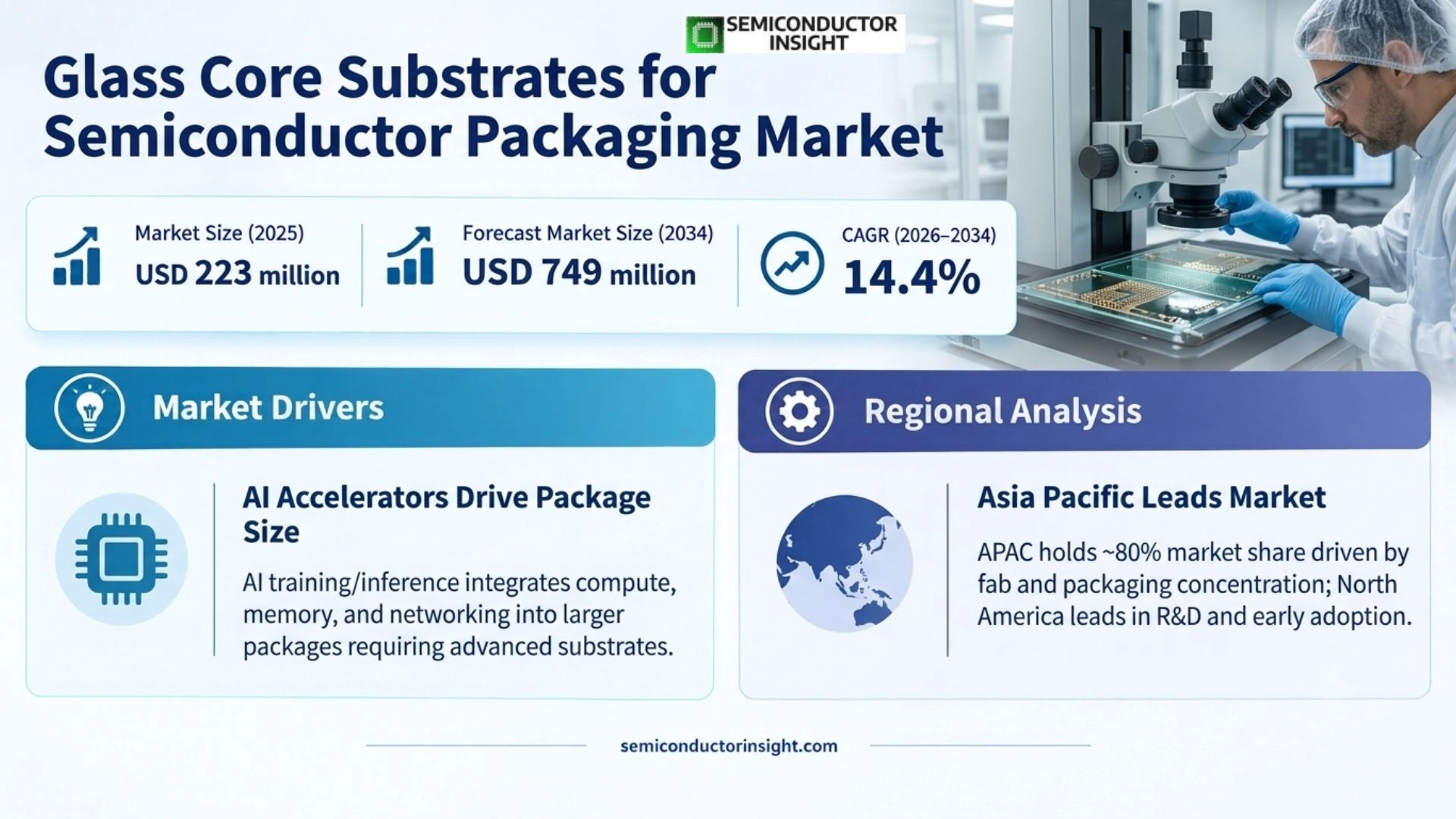
2025 Market Size
USD 223 million
2034 Projected Size
USD 749 million
CAGR (2026–2034)
14.4%
Largest Market in 2025
Asia Pacific

Key Takeaways

  • CTE above 5 ppm/°C remains the largest defined type. This segment reflects the report scope’s practical preference for glass formulations that balance dimensional stability with compatibility across package structures and adjacent materials. The commercial requirement is not simply the lowest possible thermal expansion; it is controlled expansion, surface integrity and manufacturability across repeated high-temperature processing steps.
  • Wafer-level packaging is the leading application. WLP aligns naturally with fine-pitch interconnects and thin package architectures, making glass attractive where lithography accuracy, flatness and via control become limiting. Panel-level packaging is strategically important because larger package areas can improve productivity, but it demands robust handling, warpage management and panel-scale process control before volume economics become compelling.
  • High-performance computing is the dominant end-user industry. AI accelerators, GPUs and chiplet-based systems place pressure on package size, routing density, thermal stability and signal integrity simultaneously. Intel has positioned glass substrates specifically for larger form-factor packages and higher-speed applications, while AGC and SCHOTT are developing glass technologies around fine vias, low loss and thermomechanical stability.
  • Asia Pacific is the largest regional market at 80% in the report-page scope. Its advantage comes from the concentration of semiconductor fabs, OSATs, substrate ecosystems and advanced packaging activity in Japan, South Korea, Taiwan and China. North America follows as an R&D and early-adoption centre, while Europe is smaller but relevant to specialty glass, automotive and industrial applications.
  • Qualification rather than raw glass volume is the main commercial bottleneck. The material must satisfy CTE, flatness, strength, dielectric behaviour, surface quality and through-glass-via processability simultaneously. Suppliers therefore need deep process-development capabilities and customer co-engineering, while packaging customers need evidence that glass can move from pilot lots to repeatable production without adding unacceptable breakage, yield loss or handling complexity.

Glass Core Substrates for Semiconductor Packaging Market Overview

glass core substrates for semiconductor packaging market market was valued at USD 195 million in 2024 and is projected to reach USD 572 million by 2032. On the 2025–2034 reporting window, the market corresponds to USD 223 million in 2025 and USD 749 million by 2034, representing a 14.4% CAGR during 2026–2034. Asia Pacific is the largest regional market, with the report page assigning it an 80% share in 2024.

Glass core substrates replace or supplement organic package-core materials with glass as the mechanically and electrically stable foundation of an advanced semiconductor package. The commercial proposition is tied to the packaging limits created by larger chiplet assemblies, more demanding power delivery and tighter routing. Glass combines high rigidity with excellent surface flatness, dimensional stability, electrical insulation and controllable thermal expansion, which allows package designers to pursue larger footprints and finer interconnect structures without relying entirely on the mechanical behaviour of organic laminates.

The addressable scope includes glass systems used as core or carrier structures in advanced semiconductor packaging, including material preparation, precision thinning, surface finishing, via formation and associated metallization pathways needed to convert flat glass into a functional package substrate. The report segmentation is organized by CTE above or below 5 ppm/°C, by wafer-level or panel-level packaging, and by end-user industry covering artificial intelligence hardware, high-performance computing, 5G infrastructure, automotive electronics and consumer electronics. These boundaries matter because carrier glass used only as a temporary support is commercially adjacent but not identical to a permanent package-core solution.

Demand is created when package designers run into limits on organic substrate size, warpage, dimensional accuracy or signal integrity. Intel states that glass can enable very large package form factors and up to a 10x increase in interconnect density in targeted advanced-packaging designs, while AGC highlights rigidity, flatness, fine via processability, thermal and mechanical stability, low electrical loss and insulation as key advantages. The technology response is therefore a materials-and-process shift: suppliers must provide the right glass chemistry, processing route and surface condition, while packaging houses must adapt equipment, laser drilling, metallization and inspection to the new substrate behaviour.

The market is changing now because AI and high-performance computing are forcing more functionality into single packages while reducing the design margin available to conventional substrate materials. Intel announced a glass-substrate platform in 2023 for planned commercialization in the latter half of the 2020s, and AGC has described full-scale development of glass-core substrates for next-generation packages. Those moves convert glass from a laboratory material into a strategic substrate candidate, increasing spending on process qualification, sample lines, equipment compatibility and supplier capacity before broad volume adoption begins.

Segment Analysis: By Type

By type, the market is divided into Coefficient of Thermal Expansion (CTE), above 5 ppm/°C and Coefficient of Thermal Expansion (CTE), below 5 ppm/°C. The report page identifies the above-5 ppm/°C group as dominant because it balances thermal stability with compatibility requirements across heterogeneous package constructions, whereas below-5 ppm/°C glass is better positioned where closer matching to low-expansion semiconductor structures becomes the primary design objective.

Type Functional role Market position
CTE above 5 ppm/°C Provides controlled thermal expansion while retaining the mechanical stability, flatness and insulating behaviour required for advanced package structures. The selection can reduce warpage relative to organic materials while avoiding an excessively narrow process window. Largest type in the report scope. Commercial demand is tied to broad packaging compatibility, manufacturability and the ability to integrate glass into heterogeneous packages without requiring every adjacent material to be redesigned at once.
CTE below 5 ppm/°C Provides a lower-expansion platform for applications that place greater emphasis on dimensional matching and thermomechanical alignment with silicon-rich structures. Its value rises as package sizes grow and fine-pitch features become more sensitive to cumulative movement during heating. A specialised growth segment. Adoption is constrained by formulation, process and customer-qualification requirements, but it has strong relevance for high-density AI and HPC packages where overlay accuracy and low warpage can justify higher material and process complexity.

Pricing and specification logic by CTE

Glass pricing is shaped less by commodity glass tonnage than by the degree of precision required after forming. A package supplier buying ordinary display-grade sheet cannot simply convert it into a semiconductor core without additional process control. Surface roughness, thickness variation, edge quality, internal stress, laser response, dielectric behaviour and via-wall geometry determine the usable value of the material. Lower-CTE or higher-uniformity grades therefore command greater engineering attention, while volume economics depend on how quickly the process can move from small panels and sample wafers to repeatable package-scale manufacturing.

Segment Analysis: By Application

By application, the report scope includes Wafer Level Packaging and Panel Level Packaging. Wafer-level packaging is the leading application because it aligns with established semiconductor process flows and provides a direct pathway for fine-pitch, thin-profile and high-density package architectures. Panel-level packaging represents a larger-area productivity opportunity, but requires more mature handling, metrology and warpage controls before the full economic benefit can be captured.

Application Demand characteristics
Wafer Level Packaging Purchasing is triggered when package designers need high interconnect density, stable overlay, low warpage and tight process control on wafer-scale manufacturing. Glass responds through flatness, rigidity and fine-via capability. The commercial implication is that suppliers must prove compatibility with lithography, bonding, drilling, metallization and inspection equipment while maintaining consistent thickness and surface quality over repeated production lots.
Panel Level Packaging Demand is driven by the need to improve throughput and spread packaging cost across larger formats. Glass panels can provide mechanically stable large-area platforms, but panel handling creates additional requirements for breakage resistance, thickness uniformity, edge strength and automated inspection. Suppliers able to combine large-panel availability with reliable processing and handling are better placed to support OSAT and foundry adoption as panel-level flows mature.

End-user industry lens

End-user demand is segmented into Artificial Intelligence Hardware, High-Performance Computing, 5G Infrastructure, Automotive Electronics and Consumer Electronics. High-performance computing is the dominant industry in the report scope, while AI hardware is the most important strategic growth vector because the rise of chiplets increases both package size and the number of high-speed connections that a substrate must route without excessive distortion or loss.
Glass Core Substrates for Semiconductor Packaging Market Share

Regional Analysis

Asia Pacific is the largest regional market at 80% in the report-page scope and is the fastest-growing commercial centre, supported by the concentration of semiconductor fabrication, advanced packaging and specialty-glass capability. North America is the strongest R&D and early-adoption market, Europe is a specialty and automotive-driven niche, South America remains import-dependent, and Middle East & Africa is an emerging market with selective AI and electronics investment.

How does regional demand differ across the glass-core substrate value chain?

Regional demand differs because each geography occupies a different position in the advanced-packaging ecosystem. Asia Pacific combines substrate manufacturing, wafer fabrication and OSAT demand, so glass qualification can move directly from material development into production engineering. North America has stronger influence over package architecture and AI system design, making it important for early customer specifications even when physical manufacturing occurs elsewhere. Europe is oriented toward specialty glass and automotive reliability. South America depends on imported semiconductor materials, while the Middle East and Africa are developing demand around data infrastructure and advanced electronics rather than local package-material production.

Region Position Growth outlook Demand profile Supplier-selection gate
Asia Pacific Largest Highest Fab and OSAT led Process qualification, local engineering support, high-volume consistency
North America Second Very high AI/HPC and R&D led Package design collaboration, U.S. supply resilience, advanced metrology
Europe Third Moderate Automotive, specialty and industrial Reliability, specialty glass expertise, regulatory compliance
South America Fourth Emerging Import and assembly led Landed cost, distributor support, application engineering
Middle East & Africa Smallest Emerging Data infrastructure and selective high-reliability Supply reliability, technical support, project-based qualification

Detailed Regional Blocks

Asia Pacific LARGEST & FASTEST-GROWING

Why does Asia Pacific lead the glass-core substrate market?

Asia Pacific leads because the region combines the highest concentration of semiconductor manufacturing, advanced packaging and specialty-glass suppliers. The report page assigns an 80% share to Asia Pacific, and the commercial logic is reinforced by Japan, South Korea, Taiwan and China occupying complementary positions across materials, fabs, OSATs and electronics. Suppliers can therefore shorten qualification cycles by placing engineering and sampling close to the customers that will ultimately consume the substrate.

Market positionLargest region
Growth outlookHighest
Demand profileFab and OSAT led
Market access gateLocal process engineering
Country Position in region What drives demand
Japan Core materials base AGC, Hoya and Ohara provide specialty-glass expertise close to advanced semiconductor manufacturing. Demand is driven by packaging R&D, precision optics-to-semiconductor process transfer, automotive electronics and the region’s established materials-engineering culture.
South Korea Advanced memory and package ecosystem High-density semiconductor production creates demand for substrate solutions that can support larger packages and fine routing. Collaboration with major memory and logic suppliers is important because glass adoption will depend on package qualification rather than material availability alone.
Taiwan Leading foundry and OSAT hub The concentration of foundries and outsourced assembly gives Taiwan outsized influence over future package standards. Suppliers must demonstrate repeatable via formation, warpage control and integration with advanced packaging lines to gain acceptance.
China Large electronics and packaging base China combines a large domestic electronics industry with expanding semiconductor manufacturing capability. Local sourcing, cost control and supply-chain resilience are important, while export-control exposure makes qualification of regional materials increasingly strategic.
India Emerging semiconductor investment New semiconductor and packaging investment is creating a future qualification market rather than a mature glass-core demand base. Early supplier engagement can establish design-in relationships before package-material standards become fixed.

Market instances

  • September 2023 – Intel announced an advanced glass-substrate platform after more than a decade of research, targeting larger packages and higher interconnect density later in the decade. The announcement matters because it pulls glass into mainstream package roadmaps and creates a qualification signal for Asian foundries, OSATs and materials suppliers serving future production. Intel
  • 2024 – AGC described full-scale development of glass-core substrates for next-generation semiconductor packages and identified fine via drilling below 100 microns as a key processing requirement. The development matters because it shows that glass adoption depends on joint materials and precision-processing capability, increasing the value of suppliers that can provide both formulation and process engineering. AGC
  • 2024 – SCHOTT introduced low-loss glass with a dielectric constant of 4.0 and dielectric loss tangent of 0.0021 at 10 GHz for high-frequency semiconductor applications. The product matters because package materials are increasingly evaluated for signal integrity as well as mechanical stability, widening the addressable opportunity for glass systems in high-speed interconnects. SCHOTT

The regional commercial logic is integration density: material suppliers sit closer to package qualification teams, semiconductor fabs and OSAT operations, allowing process issues to be resolved faster and qualification samples to move through engineering cycles without the delay associated with distant sourcing. This proximity can shorten the route from prototype glass to repeat production orders.

North America STRONGEST R&D / EARLY ADOPTION

Why is North America strategically important despite a smaller installed market?

North America is strategically important because package architecture for AI and HPC is heavily influenced by U.S. chip designers, foundries and advanced-packaging development teams. Intel’s 2023 glass-substrate announcement is a clear indicator that substrate technology is being developed as part of future package architecture, not treated as a commodity material. For suppliers, a U.S. design win can shape demand that is ultimately manufactured in Asia.

Market positionSecond
Growth outlookVery high
Demand profileAI/HPC and R&D led
Market access gateArchitecture qualification
Country Position in region What drives demand
United States Largest within region The U.S. is the leading R&D and design-in centre for AI and HPC packaging. Intel’s glass-substrate program shows that package architecture, not only substrate production, is being developed locally, increasing the importance of co-engineering and long-term ecosystem partnerships.
Canada Specialty and research market Demand is concentrated in research, photonics and advanced electronics rather than large package manufacturing. Suppliers can use Canadian programs and university ecosystems to validate material and process concepts, but commercial volumes remain linked to U.S. and Asian manufacturing decisions.
Mexico Electronics manufacturing adjacency Mexico contributes through electronics assembly and supply-chain localisation. Glass-core demand is still downstream and import dependent, making distributor availability and packaging-service relationships more important than local glass melting capacity in the near term.

Market instances

  • September 2023 – Intel publicly positioned glass substrates for data-center, AI and graphics packages and stated that targeted designs could achieve a 10x increase in interconnect density. The event matters commercially because North American package architecture teams can set requirements that cascade into Asian manufacturing supply chains, making U.S. design wins strategically important for global glass suppliers. Intel
  • November 2023 – Intel published a technical discussion explaining that switching from organic to glass substrates requires the substrate industry to remap handling and process infrastructure. This matters because adoption is not simply a material substitution; it creates equipment, process-development and training demand, rewarding suppliers able to support complete qualification programs rather than only ship glass panels. Intel
  • 2025 – Corning continues to market advanced-packaging glass carriers with CTE options from 3.4 to 9.5 and reports shipments of hundreds of thousands of wafers to top-tier customers. While carriers are adjacent to permanent glass cores, this installed process know-how reduces the learning curve for future glass-based packaging and strengthens the role of U.S. glass technology in advanced-packaging supply chains. Corning

North America’s commercial logic is design authority: winning a substrate specification with a major package architect can create downstream demand across multiple Asian production sites, because package standards and material requirements are often defined well before high-volume assembly is established. Suppliers that influence the architecture stage can therefore shape the eventual global bill of materials.

Europe SPECIALTY / AUTOMOTIVE FOCUS

Why does Europe remain relevant with a smaller market share?

Europe remains relevant because its semiconductor value chain contains high-value automotive, industrial and specialty-electronics applications where reliability, thermal cycling and material consistency matter more than simple volume. SCHOTT’s semiconductor-focused glass work and its specialty-glass heritage position the region as a technical centre for materials qualification. The commercial opportunity is therefore concentrated in demanding applications that can tolerate premium engineering content.

Market positionThird
Growth outlookModerate
Demand profileAutomotive and specialty
Market access gateReliability qualification
Country Position in region What drives demand
Germany Specialty and automotive centre Germany’s semiconductor demand is heavily linked to automotive and industrial systems. Glass-core suppliers can differentiate through reliability data, thermal cycling capability and controlled materials for packages that must operate in demanding environments.
France Research and aerospace ecosystem France offers advanced packaging, photonics and aerospace research activity. The commercial route for glass-core suppliers is through qualification programs and specialty packages, where technical performance can justify lower-volume but higher-value adoption.
Netherlands High-value semiconductor equipment ecosystem The Netherlands exerts influence through semiconductor equipment and lithography leadership. Glass-core adoption benefits from this ecosystem because fine-via and high-precision substrate processing must work with similarly stringent overlay and inspection requirements.

Market instances

  • August 2024 – SCHOTT launched low-loss specialty glass for 5G/6G, high-speed digital, RF and microwave applications, citing an er of 4.0 and tan d of 0.0021 at 10 GHz. The development matters because Europe’s specialty-glass capability is extending directly into high-frequency semiconductor material requirements, creating a differentiated route beyond commodity substrate competition. SCHOTT
  • 2024 – SCHOTT expanded semiconductor-focused technical education around glass, including thermomechanical stability, fine-pitch interconnects and heterogeneous integration. The development matters because the adoption barrier is partly an engineering knowledge gap, so suppliers that invest in application support can reduce customer risk and speed qualification. SCHOTT
  • 2024 – The European semiconductor policy environment continued to emphasise manufacturing resilience and strategic technology capacity. For glass-core suppliers, the significance is indirect but important: advanced packaging is increasingly viewed as part of semiconductor sovereignty, improving the commercial case for locally supported specialty-material development. European Commission

Europe’s commercial logic is performance-led specialization: suppliers can win smaller programs when the glass formulation solves a reliability, thermal-cycling or package-integration problem that ordinary organic materials cannot address cleanly. Specialty automotive and industrial applications can support premium technical content even when regional package volumes are lower than in East Asia.

South America EMERGING / IMPORT DEPENDENT

How is glass-core demand developing in South America?

South America is an emerging market because its semiconductor manufacturing base is smaller and much of the advanced electronics stack is imported. Glass-core substrates will therefore enter through imported packaged devices, local electronics assembly and selected research programs. The supplier response should emphasize technical documentation, distributor stock and predictable import logistics rather than duplicating the capital-intensive glass-processing infrastructure being developed in major Asian and North American centres.

Market positionFourth
Growth outlookEmerging
Demand profileImport and assembly led
Market access gateDistributor qualification
Country Position in region What drives demand
Brazil Largest regional demand base Brazil is the largest likely electronics and semiconductor demand centre in the region, but glass-core substrates are primarily imported. Local customers therefore prioritise predictable supply, technical documentation and distributor support over local material production.
Argentina Smaller specialized demand Demand is driven mainly by industrial electronics, communications and research programs. Suppliers face currency and logistics variability, so smaller batch qualification and distributor-led support are more practical routes than immediate local manufacturing.
Chile Technology and infrastructure niche Chile has advanced telecommunications and data infrastructure demand but a comparatively small semiconductor manufacturing base. Glass-core use is therefore tied to imported advanced electronics and selected packaging or photonics programs rather than domestic substrate volume.

Market instances

  • 2024–2026 – Brazil continued expanding digital infrastructure and advanced electronics demand, while local semiconductor manufacturing remained smaller than the major Asian and North American ecosystems. The implication for glass-core suppliers is that near-term demand is likely to arrive through imported advanced semiconductor packages and electronics, making distributor relationships and technical documentation more important than local glass-core production investment. Brazil government
  • 2025 – Telecommunications and data-infrastructure investment across Latin America continued to increase the need for higher-performance computing equipment. The market impact for glass-core substrates is indirect: higher-value servers and accelerators can pull demand for advanced packages, but suppliers still need to work through imported semiconductor and packaging channels before regional manufacturing scale becomes meaningful. ECLAC
  • 2025 – Semiconductor and electronics supply chains in South America remained dependent on imported high-value components. This creates an access-driven market in which the winning supplier is the one that can maintain availability, documentation and engineering support across distributors, rather than the company that simply offers the lowest glass-material price. OECD

South America’s commercial logic is access rather than process leadership: reliable imports, regional inventory, technical documentation and application engineering matter more than local glass production in the current phase. Buyers are likely to qualify advanced substrate materials through imported packages and local assembly relationships before any large domestic processing footprint becomes commercially justified.

Middle East & Africa SELECTIVE / PROJECT LED

Where can glass-core suppliers find the strongest opportunity in Middle East & Africa?

The strongest opportunity is concentrated around Israel’s semiconductor and AI ecosystem and the Gulf states’ investments in data infrastructure. The market remains small because local semiconductor packaging capacity is limited, but high-performance computing investment can create demand for advanced packaged devices with greater interconnect density. Suppliers should approach the region through system designers, packaging partners and infrastructure projects rather than expecting immediate large-scale substrate consumption.

Market positionSmallest
Growth outlookEmerging
Demand profileProject and AI led
Market access gateSupply reliability
Country Position in region What drives demand
Israel Advanced semiconductor and AI niche Israel’s strength in AI, accelerators and semiconductor design creates strategic demand for high-performance packaging materials even without a large domestic glass-substrate manufacturing industry. Suppliers can gain influence by partnering early with package designers and research organisations.
United Arab Emirates Data-centre and electronics investment The UAE’s digital infrastructure investment supports long-term demand for high-performance computing systems. Near-term glass-core consumption is indirect, but expanding AI infrastructure can increase the local market for advanced packaged semiconductors and associated supply-chain services.
Saudi Arabia Digital infrastructure and localization Saudi Arabia’s investment in digital infrastructure creates demand for modern computing systems and localised technology ecosystems. Glass-core substrates are likely to enter through imported advanced packages initially, with local assembly and electronics programs providing a later qualification pathway.

Market instances

  • 2025 – Gulf states continued investing in data centers, AI infrastructure and digital platforms, increasing the installed base of high-performance computing systems that ultimately depend on advanced semiconductor packaging. The immediate market effect is downstream rather than local substrate fabrication, creating demand for engineering support around imported high-end packages and system qualification. Saudi Ministry of Communications
  • 2025 – Israel remained a major semiconductor design and AI ecosystem, with advanced compute architectures creating requirements for higher-density packaging. The commercial impact is a stronger design-in opportunity for glass materials even when manufacturing occurs overseas, because package specifications can originate with Israeli or U.S.-linked technology developers. Israel Innovation Authority
  • 2025 – UAE investment in advanced digital infrastructure continued to expand the region’s capacity for AI and cloud workloads. For glass-core suppliers, this improves the long-term addressable market for advanced packaged accelerators and networking devices, although direct substrate consumption remains tied to imported semiconductor manufacturing supply chains. UAE Government

The regional commercial logic is selective qualification: suppliers can establish strategic positions through AI, semiconductor design and high-reliability projects even before local substrate manufacturing becomes substantial. Early design influence can matter disproportionately in markets where semiconductor packaging is imported, because a qualified material can travel with the packaged device into multiple infrastructure and electronics projects.

Competitive Landscape

Competition in glass-core substrates is determined by a combination of glass chemistry, precision forming, via processing, flatness control, thermal behaviour, reliability engineering and customer qualification. The market is concentrated among established specialty-glass manufacturers, but the commercial test is whether a supplier can turn a laboratory material into a repeatable package substrate that survives high-volume process windows. Companies with application-engineering resources and existing semiconductor relationships have an advantage because qualification can span materials, equipment and package design simultaneously.

The established glass suppliers compete by differentiating the material itself and the processing route used to convert it into a semiconductor-grade core. AGC emphasises the combination of glass expertise and advanced processing, while SCHOTT highlights specialty-glass know-how, TGV development and application engineering. Corning brings an installed base in precision glass carriers and advanced packaging, while Japanese companies such as Hoya and Ohara add precision-material capability and proximity to the Asian semiconductor ecosystem. The buyer is therefore purchasing a process-capable platform rather than a sheet of glass.

Customer qualification is especially important because advanced packaging programs are multi-year design cycles. Once a substrate chemistry, via process, metallization stack and dimensional tolerance are qualified, switching suppliers can require new reliability tests, process windows and package-level validation. This raises the value of first-mover technical collaboration and creates a barrier to commodity-style competition even if multiple suppliers can meet a nominal glass composition. Pricing becomes secondary when a package line depends on stable yield and uninterrupted access to qualified material.

The competitive landscape is also expanding toward adjacent photonics and temporary-carrier applications. SCHOTT’s low-loss glass and Corning’s advanced packaging carriers show how optical loss, CTE and ultra-flat surfaces can become stepping stones toward broader glass adoption. Suppliers that already understand laser processing, fine vias and semiconductor cleanliness can leverage those capabilities into permanent glass-core programs, while new entrants face a steeper learning curve in reliability and manufacturing control.

Key Industry Players

  • AGC Inc.
  • SCHOTT AG
  • Corning Incorporated
  • Hoya Corporation
  • Ohara Inc.
  • Dai Nippon Printing (DNP)
  • Nippon Electric Glass (NEG)
  • CrysTop Glass
  • WGTech

Production Capacity Analysis

Production capacity is constrained less by raw glass melting capacity than by semiconductor-grade precision processing. The critical bottlenecks are low-defect glass production, thickness and flatness control, laser or other via formation, metallization compatibility, edge strength, handling and inspection. A supplier that can make large glass panels but cannot maintain yield after drilling and metallization does not have economically usable capacity. Capacity therefore expands through process qualification as much as through additional furnaces or drawing lines.

Where capacity is concentrated

Capacity development is concentrated in Japan, Europe, the United States and parts of East Asia where specialty-glass companies already operate high-precision manufacturing and semiconductor customer programs. Asia Pacific has the largest end-market pull, but North American and European technology developers retain strategic importance because glass-core architectures are still being defined.

What actually constrains output

The constraint is the conversion of glass into a package-ready substrate. AGC identifies sub-100-micron via drilling as a technical requirement, while Corning and SCHOTT emphasise surface quality, CTE control and process reliability. Each processing step adds yield sensitivity, so usable capacity can grow more slowly than nominal glass output. The practical bottleneck is repeatable semiconductor-grade processing rather than raw glass tonnage.

Upstream concentration risk

Upstream risk includes specialty glass compositions, precision processing equipment, lasers, metallization chemistries and inspection systems. Because package materials are qualified together with process parameters, customers can be reluctant to dual-source early in a product cycle. That creates a temporary concentration risk in both material supply and technical know-how, particularly for the most demanding AI and HPC applications.

Market Dynamics

The glass-core substrate market is in a qualification-led growth phase: package designers are increasing chiplet density and package size, glass suppliers are proving precision processing, and semiconductor manufacturers are building the process infrastructure needed to move from prototypes into volume. Demand is strongest where organic substrates encounter mechanical, electrical or dimensional constraints, while adoption is slowed by higher processing complexity, brittle-material handling and the need to redesign parts of established package manufacturing lines.

Market Drivers

Primary market drivers and commercial impact

Factor Relative impact* Commercial mechanism
AI and HPC package scaling High Larger chiplet packages raise the need for low-warpage, high-flatness substrates and more precise interconnect routing. Suppliers that qualify glass with leading-edge package designers can capture design wins before volume manufacturing starts.
Higher interconnect density High Intel’s targeted glass designs point to up to 10x interconnect-density improvement in relevant architectures. The commercial value is strongest where package routing, power delivery and signal integrity become the limiting factors.
Heterogeneous integration High As packages combine chiplets and different dies, controlled CTE, rigidity and dimensional stability reduce mechanical risk. This increases the value of glass formulations engineered for multi-material package stacks.
Panel-level productivity Medium Larger panels can improve throughput and reduce handling cost per package, but the benefit becomes commercial only when panel breakage, metrology and warpage are controlled at high yield.

AI accelerators increase package dimensions

AI training and inference accelerators increasingly combine compute, memory and networking functions in large packages. This requirement creates a substrate problem before it creates a glass problem: the package must remain flat and dimensionally stable while carrying many high-speed connections. Glass responds with rigidity and flatness, suppliers respond through large-format process development, and the market implication is that AI architecture decisions can pull glass demand years before final package volumes are visible.

Fine-pitch routing turns flatness into a commercial parameter

When interconnect pitch becomes tighter, small substrate distortions can reduce process margin and complicate lithography or assembly alignment. Glass is attractive because its stiffness and surface quality can support more stable fine-feature processing than flexible organic materials. The supplier response therefore includes not just glass chemistry but polishing, thickness control and inspection; the commercial implication is that high-value contracts will increasingly be awarded on process capability rather than material price.

Heterogeneous integration expands material requirements

Chiplet architectures increase the number of materials and interfaces inside a package. Glass helps by offering predictable dimensional behaviour and electrical insulation, which reduces some interactions between copper, silicon and organic layers. Suppliers must consequently develop grades tuned to specific package stacks, while OSATs and foundries need new reliability evidence. The market expands when customers accept glass as an engineered platform rather than a universal material substitute.

Photonic integration broadens the addressable use case

Glass has optical transparency and can support embedded photonic structures, creating a route into co-packaged optics and silicon-photonics architectures. This expands the market beyond conventional electronic routing. Suppliers with both optical and semiconductor-material expertise can reuse precision-glass capabilities, while package designers gain a material that can carry electrical and optical functions in closer proximity.

Market Restraints

Primary restraints and commercial impact

Factor Relative impact* Commercial mechanism
Higher processing complexity High TGV formation, metallization, finishing and inspection increase capital and yield requirements relative to mature organic substrates.
Brittleness and handling risk Medium Glass can chip or fracture during handling and thermal cycling, increasing the burden on equipment adaptation and process control.
Qualification cycle length High Package customers must validate material, process, reliability and assembly behaviour together, delaying supplier switches and new capacity ramps.
Limited installed manufacturing infrastructure Medium Existing substrate factories are optimised for organic materials, so glass adoption can require equipment, tooling and workforce changes.

Brittleness raises handling cost

Glass offers stiffness and flatness but remains less forgiving of impact and edge damage than many organic substrates. That creates a requirement for controlled transport, edge protection, automated handling and process-specific inspection. Equipment suppliers and substrate makers must redesign fixtures where necessary, while customers must accept additional qualification expense. The commercial implication is that the fastest adoption will occur where the performance gain clearly outweighs incremental handling and yield costs.

TGV processing is yield-sensitive

Through-glass vias require precise drilling, cleaning and metallization. AGC describes laser-based via drilling below 100 microns as an important requirement, illustrating how the process window can be narrower than conventional substrate fabrication. Every percentage point of yield lost through drilling, breakage or metallization directly affects usable capacity. Suppliers therefore compete on process control, not merely on glass chemistry, and buyers care about repeatability across lots.

Legacy infrastructure slows substitution

Organic-substrate production lines have years of investment in equipment, tooling, recipes and operator training. Moving to glass requires changes in handling and process controls, so customers will adopt it first in packages where the incumbent material is already becoming a hard constraint. This makes glass a performance-led substitution cycle rather than a low-friction cost-reduction project, slowing volume conversion even when the technical case is strong.

Customer concentration can amplify risk

The early glass-core market depends on a relatively small set of leading semiconductor manufacturers, foundries and advanced-packaging programs. A supplier may therefore invest heavily in qualification for one package family without a guaranteed multi-customer volume base. Commercial success requires platforms that can be adapted across customers and package geometries so that qualification spending creates a reusable capability rather than a single-program asset.

Market Opportunities

Priority commercial opportunities

AI and HPC package platforms

Where: U.S. and Asian leading-edge packaging ecosystems. Who benefits: specialty-glass makers, TGV process developers, metrology suppliers and OSATs. What changes: package size, chiplet count and routing density increase, making flatness and CTE control more valuable. Commercial implication: early co-development agreements can secure recurring material demand when a validated package platform progresses from engineering lots into volume manufacturing and the material specification becomes embedded in production recipes.

Panel-level packaging

Where: Asia Pacific packaging clusters. Who benefits: large-format glass producers, handling-equipment makers and panel-processing specialists. What changes: package production shifts from wafer-scale to larger formats, raising throughput potential but also handling and warpage requirements. Commercial implication: suppliers that solve panel breakage and metrology can capture both substrate and process-equipment value.

Optical and co-packaged interfaces

Where: North America, Europe and advanced Asian photonics hubs. Who benefits: glass suppliers with optical expertise and semiconductor package developers. What changes: electrical routing increasingly sits beside optical paths and high-speed links. Commercial implication: low-loss, transparent and dimensionally stable glass can become a common platform for mixed electronic-photonic packaging, allowing one materials ecosystem to address both signal integrity and mechanical stability requirements.

Automotive and high-reliability packages

Where: Europe, Japan, Korea and North America. Who benefits: specialty-glass producers and package houses with reliability testing capability. What changes: package materials are judged over temperature cycles, vibration and long service life. Commercial implication: suppliers can defend premium pricing when they provide reliable CTE, mechanical stability and documented process control for high-value systems.

Supply Chain Analysis

1. Glass composition & formingSpecialty glass raw materials → melting/forming → controlled sheet or panel
2. Precision processingCutting → grinding/polishing → thickness/flatness control → surface treatment
3. TGV & metallizationLaser or other via formation → cleaning → dielectric/metal stack → inspection
4. Package integrationSubstrate qualification → die/package assembly → reliability testing → production ramp

Glass composition and forming

Value capture starts with the glass formulation because thermal expansion, rigidity, dielectric behaviour and laser response are established before semiconductor processing begins. Specialty-glass suppliers capture the highest upstream technical value when they can tailor composition to package requirements. Bottlenecks arise when a package needs unusually tight CTE or defect specifications because only a small group of suppliers can simultaneously guarantee material consistency and semiconductor cleanliness.

Precision processing

The second stage converts bulk glass into package-ready stock. Thickness, flatness, surface roughness, edge strength and dimensional tolerances determine whether downstream via and metallization steps can run reliably. Processing suppliers and glass makers therefore compete on metrology and yield as much as throughput. The bottleneck is often small variation across a panel rather than the absolute ability to manufacture a large panel.

TGV formation and metallization

TGV creation is a critical value-capture point because it turns an insulating glass core into a routed semiconductor substrate. Laser drilling, cleaning, dielectric isolation and copper or other metallization must work as one process chain. The commercial bottleneck is yield: a process that produces excellent individual vias but generates too much chipping, taper variation or contamination cannot support high-volume package economics.

Package integration and qualification

Final value is captured when the substrate becomes part of a qualified package and then a production product. Foundries, OSATs and system companies validate signal integrity, thermal cycling, mechanical reliability and manufacturing yield. This is where supplier lock-in can emerge because switching the substrate can require requalification of multiple process steps. The winning supply chain is therefore the one that combines materials with application engineering and reliability support.

Recent Developments

18 September 2023

Intel announced industry-leading glass substrates for next-generation advanced packaging, highlighting larger form factors, improved flatness, and a target of up to 10x interconnect density in relevant designs. The development matters because a major processor manufacturer publicly tied glass to future package scaling, raising the probability of broader supplier qualification and accelerating ecosystem investment around materials, equipment and process development. Source

2024

AGC described full-scale development of glass-core substrates and highlighted sub-100-micron laser-via processing plus six material advantages including rigidity, flatness, fine processability, thermal stability, low electrical loss and insulation. The development matters because it shows that glass-core economics depend on tightly integrated material and process engineering, not simply on access to specialty glass. Source

30 August 2024

SCHOTT launched low-loss glass with a dielectric constant of 4.0 and dielectric loss tangent of 0.0021 at 10 GHz for advanced packaging and high-frequency applications. The development expands the competitive basis of glass from mechanical stability into signal-integrity performance and creates a path for specialty-glass suppliers to address faster electrical links and mixed electronic-photonic systems. Source

2025

Corning continued positioning advanced-packaging glass carriers around ultra-flat surfaces, controlled CTE and high-volume semiconductor handling, reporting hundreds of thousands of wafers shipped to top-tier customers. The commercial significance is that mature carrier operations can reduce process-learning risk for broader glass packaging adoption by providing customers with an established handling and bonding ecosystem. Source

Report Scope & Segmentation

Attribute Details
Report title Glass Core Substrates for Semiconductor Packaging Market Size, Trends, Business Strategies 2026-2034.
2025 market size USD 223 million
2034 projected size USD 749 million
CAGR 14.4% for 2026–2034.
By Type Coefficient of Thermal Expansion (CTE), above 5 ppm/°C; Coefficient of Thermal Expansion (CTE), below 5 ppm/°C.
By Application Wafer Level Packaging; Panel Level Packaging.
By End User Artificial Intelligence Hardware; High-Performance Computing; 5G Infrastructure; Automotive Electronics; Consumer Electronics.
Regions Asia-Pacific; North America; Europe; South America; Middle East & Africa.
Company universe AGC Inc.; SCHOTT AG; Corning Incorporated; Hoya Corporation; Ohara Inc.; Dai Nippon Printing (DNP); Nippon Electric Glass (NEG); CrysTop Glass; WGTech.

Frequently Asked Questions

What is the 2025 market size?

The global glass core substrates for semiconductor packaging market corresponds to USD 223 million in 2025 for 2025. The market is positioned in advanced semiconductor packaging, where glass is used to improve dimensional stability, flatness, routing density and related package-performance attributes. The commercial trajectory depends on advanced-package adoption, qualification progress and expansion from development programs into production platforms.

What is the projected 2034 market size?

The market is projected at approximately USD 749 million by 2034 on the 2025–2034 window. The increase is associated with higher adoption of advanced packaging for AI, HPC, chiplets and other high-density architectures in which organic substrate limitations become increasingly important. The value increase depends on greater substrate content per advanced package as AI, high-performance computing and chiplet architectures expand in volume and complexity.

What CAGR applies during 2026–2034?

The reporting-window CAGR is 14.4% for 2026–2034. The growth profile reflects an early-stage market in which commercial expansion depends on customer qualification, package-design adoption, capacity ramping and the conversion of glass from prototype material into repeatable production substrate. The rate reflects a transition from early engineering activity toward repeatable commercial adoption across advanced semiconductor packaging programs.

Which type leads the market?

CTE above 5 ppm/°C is the leading type in the report scope. Its commercial advantage is that it offers a practical balance of thermal expansion, dimensional stability and compatibility with heterogeneous package structures, making it easier to integrate into a broader range of advanced packaging designs than a narrowly optimised material grade.

Which application is largest?

Wafer Level Packaging is the leading application. It aligns with established semiconductor process infrastructure and supports fine-pitch interconnects, thin package profiles and high-density architectures. Panel Level Packaging remains strategically important because it can improve larger-area productivity, but it carries greater handling, warpage and process-control requirements. The application benefits from established wafer-scale process flows and the need to control fine-feature alignment across increasingly dense package structures.

Which end-user industry dominates?

High-Performance Computing is the dominant end-user industry in the report scope. HPC and AI packages need higher interconnect density, larger package footprints and tighter thermomechanical control, which are precisely the conditions in which glass-core substrates can provide a differentiated advantage relative to conventional organic cores. This segment places the strongest simultaneous demands on package dimensions, thermal stability, interconnect density and signal integrity.

Which region leads the market?

Asia Pacific leads the market with an 80% share in the report-page scope. The region’s strength comes from the concentration of semiconductor fabrication, OSAT activity and specialty-glass expertise across Japan, South Korea, Taiwan and China, making it the most direct route from glass qualification into high-volume semiconductor production. The region also provides the strongest combination of materials suppliers, semiconductor fabs, OSATs and electronics customers required to qualify new substrate technologies.

Why is glass being considered for advanced packaging?

Glass is being considered because its rigidity, ultra-flat surfaces, dimensional stability, electrical insulation and controllable CTE can support larger and more densely interconnected packages. Intel has highlighted larger form factors and higher interconnect density, while AGC emphasises precision via processing and thermomechanical stability as key parts of the value proposition.

What are the main restraints?

The main restraints are processing complexity, breakage risk, yield sensitivity in via formation and the qualification burden associated with changing established substrate materials. Customers must validate handling, drilling, metallization, assembly and reliability together, so suppliers with strong application engineering can reduce adoption friction and improve the likelihood of a successful production ramp.

Who are the key industry players?

The report-page company universe includes AGC, SCHOTT, Corning, Hoya, Ohara, Dai Nippon Printing, Nippon Electric Glass, CrysTop Glass and WGTech. Competition centres on specialty-glass chemistry, precision processing, surface quality, via formation, reliability engineering and the ability to support semiconductor customers from prototype qualification through volume production. Supplier differentiation is therefore based on process maturity and customer support as much as on nominal glass properties or catalogue breadth.
Glass Core Substrates for Semiconductor Packaging Market Size, Trends, Business Strategies 2026-2034

Get Sample Report PDF for Exclusive Insights

Report Sample Includes

  • Table of Contents
  • List of Tables & Figures
  • Charts, Research Methodology, and more...

PDF Icon Download Sample Report PDF

Download Sample Report

Table of Content

1 Introduction to Research & Analysis Reports
1.1 Glass Core Substrates for Semiconductor Packaging Market Definition
1.2 Market Segments
1.2.1 Segment by Type
1.2.2 Segment by Application
1.3 Global Glass Core Substrates for Semiconductor Packaging Market Overview
1.4 Features & Benefits of This Report
1.5 Methodology & Sources of Information
1.5.1 Research Methodology
1.5.2 Research Process
1.5.3 Base Year
1.5.4 Report Assumptions & Caveats
2 Global Glass Core Substrates for Semiconductor Packaging Overall Market Size
2.1 Global Glass Core Substrates for Semiconductor Packaging Market Size: 2024 VS 2032
2.2 Global Glass Core Substrates for Semiconductor Packaging Market Size, Prospects & Forecasts: 2020-2032
2.3 Global Glass Core Substrates for Semiconductor Packaging Sales: 2020-2032
3 Company Landscape
3.1 Top Glass Core Substrates for Semiconductor Packaging Players in Global Market
3.2 Top Global Glass Core Substrates for Semiconductor Packaging Companies Ranked by Revenue
3.3 Global Glass Core Substrates for Semiconductor Packaging Revenue by Companies
3.4 Global Glass Core Substrates for Semiconductor Packaging Sales by Companies
3.5 Global Glass Core Substrates for Semiconductor Packaging Price by Manufacturer (2020-2025)
3.6 Top 3 and Top 5 Glass Core Substrates for Semiconductor Packaging Companies in Global Market, by Revenue in 2024
3.7 Global Manufacturers Glass Core Substrates for Semiconductor Packaging Product Type
3.8 Tier 1, Tier 2, and Tier 3 Glass Core Substrates for Semiconductor Packaging Players in Global Market
3.8.1 List of Global Tier 1 Glass Core Substrates for Semiconductor Packaging Companies
3.8.2 List of Global Tier 2 and Tier 3 Glass Core Substrates for Semiconductor Packaging Companies
4 Sights by Product
4.1 Overview
4.1.1 Segment by Type – Global Glass Core Substrates for Semiconductor Packaging Market Size Markets, 2024 & 2032
4.1.2 Coefficient of Thermal Expansion (CTE), above 5 ppm/°C
4.1.3 Coefficient of Thermal Expansion (CTE), below 5 ppm/°C
4.2 Segment by Type – Global Glass Core Substrates for Semiconductor Packaging Revenue & Forecasts
4.2.1 Segment by Type – Global Glass Core Substrates for Semiconductor Packaging Revenue, 2020-2025
4.2.2 Segment by Type – Global Glass Core Substrates for Semiconductor Packaging Revenue, 2026-2032
4.2.3 Segment by Type – Global Glass Core Substrates for Semiconductor Packaging Revenue Market Share, 2020-2032
4.3 Segment by Type – Global Glass Core Substrates for Semiconductor Packaging Sales & Forecasts
4.3.1 Segment by Type – Global Glass Core Substrates for Semiconductor Packaging Sales, 2020-2025
4.3.2 Segment by Type – Global Glass Core Substrates for Semiconductor Packaging Sales, 2026-2032
4.3.3 Segment by Type – Global Glass Core Substrates for Semiconductor Packaging Sales Market Share, 2020-2032
4.4 Segment by Type – Global Glass Core Substrates for Semiconductor Packaging Price (Manufacturers Selling Prices), 2020-2032
5 Sights by Application
5.1 Overview
5.1.1 Segment by Application – Global Glass Core Substrates for Semiconductor Packaging Market Size, 2024 & 2032
5.1.2 Wafer Level Packaging
5.1.3 Panel Level Packaging
5.2 Segment by Application – Global Glass Core Substrates for Semiconductor Packaging Revenue & Forecasts
5.2.1 Segment by Application – Global Glass Core Substrates for Semiconductor Packaging Revenue, 2020-2025
5.2.2 Segment by Application – Global Glass Core Substrates for Semiconductor Packaging Revenue, 2026-2032
5.2.3 Segment by Application – Global Glass Core Substrates for Semiconductor Packaging Revenue Market Share, 2020-2032
5.3 Segment by Application – Global Glass Core Substrates for Semiconductor Packaging Sales & Forecasts
5.3.1 Segment by Application – Global Glass Core Substrates for Semiconductor Packaging Sales, 2020-2025
5.3.2 Segment by Application – Global Glass Core Substrates for Semiconductor Packaging Sales, 2026-2032
5.3.3 Segment by Application – Global Glass Core Substrates for Semiconductor Packaging Sales Market Share, 2020-2032
5.4 Segment by Application – Global Glass Core Substrates for Semiconductor Packaging Price (Manufacturers Selling Prices), 2020-2032
6 Sights by Region
6.1 By Region – Global Glass Core Substrates for Semiconductor Packaging Market Size, 2024 & 2032
6.2 By Region – Global Glass Core Substrates for Semiconductor Packaging Revenue & Forecasts
6.2.1 By Region – Global Glass Core Substrates for Semiconductor Packaging Revenue, 2020-2025
6.2.2 By Region – Global Glass Core Substrates for Semiconductor Packaging Revenue, 2026-2032
6.2.3 By Region – Global Glass Core Substrates for Semiconductor Packaging Revenue Market Share, 2020-2032
6.3 By Region – Global Glass Core Substrates for Semiconductor Packaging Sales & Forecasts
6.3.1 By Region – Global Glass Core Substrates for Semiconductor Packaging Sales, 2020-2025
6.3.2 By Region – Global Glass Core Substrates for Semiconductor Packaging Sales, 2026-2032
6.3.3 By Region – Global Glass Core Substrates for Semiconductor Packaging Sales Market Share, 2020-2032
6.4 North America
6.4.1 By Country – North America Glass Core Substrates for Semiconductor Packaging Revenue, 2020-2032
6.4.2 By Country – North America Glass Core Substrates for Semiconductor Packaging Sales, 2020-2032
6.4.3 United States Glass Core Substrates for Semiconductor Packaging Market Size, 2020-2032
6.4.4 Canada Glass Core Substrates for Semiconductor Packaging Market Size, 2020-2032
6.4.5 Mexico Glass Core Substrates for Semiconductor Packaging Market Size, 2020-2032
6.5 Europe
6.5.1 By Country – Europe Glass Core Substrates for Semiconductor Packaging Revenue, 2020-2032
6.5.2 By Country – Europe Glass Core Substrates for Semiconductor Packaging Sales, 2020-2032
6.5.3 Germany Glass Core Substrates for Semiconductor Packaging Market Size, 2020-2032
6.5.4 France Glass Core Substrates for Semiconductor Packaging Market Size, 2020-2032
6.5.5 U.K. Glass Core Substrates for Semiconductor Packaging Market Size, 2020-2032
6.5.6 Italy Glass Core Substrates for Semiconductor Packaging Market Size, 2020-2032
6.5.7 Russia Glass Core Substrates for Semiconductor Packaging Market Size, 2020-2032
6.5.8 Nordic Countries Glass Core Substrates for Semiconductor Packaging Market Size, 2020-2032
6.5.9 Benelux Glass Core Substrates for Semiconductor Packaging Market Size, 2020-2032
6.6 Asia
6.6.1 By Region – Asia Glass Core Substrates for Semiconductor Packaging Revenue, 2020-2032
6.6.2 By Region – Asia Glass Core Substrates for Semiconductor Packaging Sales, 2020-2032
6.6.3 China Glass Core Substrates for Semiconductor Packaging Market Size, 2020-2032
6.6.4 Japan Glass Core Substrates for Semiconductor Packaging Market Size, 2020-2032
6.6.5 South Korea Glass Core Substrates for Semiconductor Packaging Market Size, 2020-2032
6.6.6 Southeast Asia Glass Core Substrates for Semiconductor Packaging Market Size, 2020-2032
6.6.7 India Glass Core Substrates for Semiconductor Packaging Market Size, 2020-2032
6.7 South America
6.7.1 By Country – South America Glass Core Substrates for Semiconductor Packaging Revenue, 2020-2032
6.7.2 By Country – South America Glass Core Substrates for Semiconductor Packaging Sales, 2020-2032
6.7.3 Brazil Glass Core Substrates for Semiconductor Packaging Market Size, 2020-2032
6.7.4 Argentina Glass Core Substrates for Semiconductor Packaging Market Size, 2020-2032
6.8 Middle East & Africa
6.8.1 By Country – Middle East & Africa Glass Core Substrates for Semiconductor Packaging Revenue, 2020-2032
6.8.2 By Country – Middle East & Africa Glass Core Substrates for Semiconductor Packaging Sales, 2020-2032
6.8.3 Turkey Glass Core Substrates for Semiconductor Packaging Market Size, 2020-2032
6.8.4 Israel Glass Core Substrates for Semiconductor Packaging Market Size, 2020-2032
6.8.5 Saudi Arabia Glass Core Substrates for Semiconductor Packaging Market Size, 2020-2032
6.8.6 UAE Glass Core Substrates for Semiconductor Packaging Market Size, 2020-2032
7 Manufacturers & Brands Profiles
7.1 AGC
7.1.1 AGC Company Summary
7.1.2 AGC Business Overview
7.1.3 AGC Glass Core Substrates for Semiconductor Packaging Major Product Offerings
7.1.4 AGC Glass Core Substrates for Semiconductor Packaging Sales and Revenue in Global (2020-2025)
7.1.5 AGC Key News & Latest Developments
7.2 Schott
7.2.1 Schott Company Summary
7.2.2 Schott Business Overview
7.2.3 Schott Glass Core Substrates for Semiconductor Packaging Major Product Offerings
7.2.4 Schott Glass Core Substrates for Semiconductor Packaging Sales and Revenue in Global (2020-2025)
7.2.5 Schott Key News & Latest Developments
7.3 Corning
7.3.1 Corning Company Summary
7.3.2 Corning Business Overview
7.3.3 Corning Glass Core Substrates for Semiconductor Packaging Major Product Offerings
7.3.4 Corning Glass Core Substrates for Semiconductor Packaging Sales and Revenue in Global (2020-2025)
7.3.5 Corning Key News & Latest Developments
7.4 Hoya
7.4.1 Hoya Company Summary
7.4.2 Hoya Business Overview
7.4.3 Hoya Glass Core Substrates for Semiconductor Packaging Major Product Offerings
7.4.4 Hoya Glass Core Substrates for Semiconductor Packaging Sales and Revenue in Global (2020-2025)
7.4.5 Hoya Key News & Latest Developments
7.5 Ohara
7.5.1 Ohara Company Summary
7.5.2 Ohara Business Overview
7.5.3 Ohara Glass Core Substrates for Semiconductor Packaging Major Product Offerings
7.5.4 Ohara Glass Core Substrates for Semiconductor Packaging Sales and Revenue in Global (2020-2025)
7.5.5 Ohara Key News & Latest Developments
7.6 Dai Nippon Printing (DNP)
7.6.1 Dai Nippon Printing (DNP) Company Summary
7.6.2 Dai Nippon Printing (DNP) Business Overview
7.6.3 Dai Nippon Printing (DNP) Glass Core Substrates for Semiconductor Packaging Major Product Offerings
7.6.4 Dai Nippon Printing (DNP) Glass Core Substrates for Semiconductor Packaging Sales and Revenue in Global (2020-2025)
7.6.5 Dai Nippon Printing (DNP) Key News & Latest Developments
7.7 NEG
7.7.1 NEG Company Summary
7.7.2 NEG Business Overview
7.7.3 NEG Glass Core Substrates for Semiconductor Packaging Major Product Offerings
7.7.4 NEG Glass Core Substrates for Semiconductor Packaging Sales and Revenue in Global (2020-2025)
7.7.5 NEG Key News & Latest Developments
7.8 CrysTop Glass
7.8.1 CrysTop Glass Company Summary
7.8.2 CrysTop Glass Business Overview
7.8.3 CrysTop Glass Glass Core Substrates for Semiconductor Packaging Major Product Offerings
7.8.4 CrysTop Glass Glass Core Substrates for Semiconductor Packaging Sales and Revenue in Global (2020-2025)
7.8.5 CrysTop Glass Key News & Latest Developments
7.9 WGTech
7.9.1 WGTech Company Summary
7.9.2 WGTech Business Overview
7.9.3 WGTech Glass Core Substrates for Semiconductor Packaging Major Product Offerings
7.9.4 WGTech Glass Core Substrates for Semiconductor Packaging Sales and Revenue in Global (2020-2025)
7.9.5 WGTech Key News & Latest Developments
8 Global Glass Core Substrates for Semiconductor Packaging Production Capacity, Analysis
8.1 Global Glass Core Substrates for Semiconductor Packaging Production Capacity, 2020-2032
8.2 Glass Core Substrates for Semiconductor Packaging Production Capacity of Key Manufacturers in Global Market
8.3 Global Glass Core Substrates for Semiconductor Packaging Production by Region
9 Key Market Trends, Opportunity, Drivers and Restraints
9.1 Market Opportunities & Trends
9.2 Market Drivers
9.3 Market Restraints
10 Glass Core Substrates for Semiconductor Packaging Supply Chain Analysis
10.1 Glass Core Substrates for Semiconductor Packaging Industry Value Chain
10.2 Glass Core Substrates for Semiconductor Packaging Upstream Market
10.3 Glass Core Substrates for Semiconductor Packaging Downstream and Clients
10.4 Marketing Channels Analysis
10.4.1 Marketing Channels
10.4.2 Glass Core Substrates for Semiconductor Packaging Distributors and Sales Agents in Global
11 Conclusion
12 Appendix
12.1 Note
12.2 Examples of Clients
12.3 DisclaimerList of Tables
Table 1. Key Players of Glass Core Substrates for Semiconductor Packaging in Global Market
Table 2. Top Glass Core Substrates for Semiconductor Packaging Players in Global Market, Ranking by Revenue (2024)
Table 3. Global Glass Core Substrates for Semiconductor Packaging Revenue by Companies, (US$, Mn), 2020-2025
Table 4. Global Glass Core Substrates for Semiconductor Packaging Revenue Share by Companies, 2020-2025
Table 5. Global Glass Core Substrates for Semiconductor Packaging Sales by Companies, (K Sqm), 2020-2025
Table 6. Global Glass Core Substrates for Semiconductor Packaging Sales Share by Companies, 2020-2025
Table 7. Key Manufacturers Glass Core Substrates for Semiconductor Packaging Price (2020-2025) & (US$/Sq m)
Table 8. Global Manufacturers Glass Core Substrates for Semiconductor Packaging Product Type
Table 9. List of Global Tier 1 Glass Core Substrates for Semiconductor Packaging Companies, Revenue (US$, Mn) in 2024 and Market Share
Table 10. List of Global Tier 2 and Tier 3 Glass Core Substrates for Semiconductor Packaging Companies, Revenue (US$, Mn) in 2024 and Market Share
Table 11. Segment by Type – Global Glass Core Substrates for Semiconductor Packaging Revenue, (US$, Mn), 2024 & 2032
Table 12. Segment by Type – Global Glass Core Substrates for Semiconductor Packaging Revenue (US$, Mn), 2020-2025
Table 13. Segment by Type – Global Glass Core Substrates for Semiconductor Packaging Revenue (US$, Mn), 2026-2032
Table 14. Segment by Type – Global Glass Core Substrates for Semiconductor Packaging Sales (K Sqm), 2020-2025
Table 15. Segment by Type – Global Glass Core Substrates for Semiconductor Packaging Sales (K Sqm), 2026-2032
Table 16. Segment by Application – Global Glass Core Substrates for Semiconductor Packaging Revenue, (US$, Mn), 2024 & 2032
Table 17. Segment by Application – Global Glass Core Substrates for Semiconductor Packaging Revenue, (US$, Mn), 2020-2025
Table 18. Segment by Application – Global Glass Core Substrates for Semiconductor Packaging Revenue, (US$, Mn), 2026-2032
Table 19. Segment by Application – Global Glass Core Substrates for Semiconductor Packaging Sales, (K Sqm), 2020-2025
Table 20. Segment by Application – Global Glass Core Substrates for Semiconductor Packaging Sales, (K Sqm), 2026-2032
Table 21. By Region – Global Glass Core Substrates for Semiconductor Packaging Revenue, (US$, Mn), 2025-2032
Table 22. By Region – Global Glass Core Substrates for Semiconductor Packaging Revenue, (US$, Mn), 2020-2025
Table 23. By Region – Global Glass Core Substrates for Semiconductor Packaging Revenue, (US$, Mn), 2026-2032
Table 24. By Region – Global Glass Core Substrates for Semiconductor Packaging Sales, (K Sqm), 2020-2025
Table 25. By Region – Global Glass Core Substrates for Semiconductor Packaging Sales, (K Sqm), 2026-2032
Table 26. By Country – North America Glass Core Substrates for Semiconductor Packaging Revenue, (US$, Mn), 2020-2025
Table 27. By Country – North America Glass Core Substrates for Semiconductor Packaging Revenue, (US$, Mn), 2026-2032
Table 28. By Country – North America Glass Core Substrates for Semiconductor Packaging Sales, (K Sqm), 2020-2025
Table 29. By Country – North America Glass Core Substrates for Semiconductor Packaging Sales, (K Sqm), 2026-2032
Table 30. By Country – Europe Glass Core Substrates for Semiconductor Packaging Revenue, (US$, Mn), 2020-2025
Table 31. By Country – Europe Glass Core Substrates for Semiconductor Packaging Revenue, (US$, Mn), 2026-2032
Table 32. By Country – Europe Glass Core Substrates for Semiconductor Packaging Sales, (K Sqm), 2020-2025
Table 33. By Country – Europe Glass Core Substrates for Semiconductor Packaging Sales, (K Sqm), 2026-2032
Table 34. By Region – Asia Glass Core Substrates for Semiconductor Packaging Revenue, (US$, Mn), 2020-2025
Table 35. By Region – Asia Glass Core Substrates for Semiconductor Packaging Revenue, (US$, Mn), 2026-2032
Table 36. By Region – Asia Glass Core Substrates for Semiconductor Packaging Sales, (K Sqm), 2020-2025
Table 37. By Region – Asia Glass Core Substrates for Semiconductor Packaging Sales, (K Sqm), 2026-2032
Table 38. By Country – South America Glass Core Substrates for Semiconductor Packaging Revenue, (US$, Mn), 2020-2025
Table 39. By Country – South America Glass Core Substrates for Semiconductor Packaging Revenue, (US$, Mn), 2026-2032
Table 40. By Country – South America Glass Core Substrates for Semiconductor Packaging Sales, (K Sqm), 2020-2025
Table 41. By Country – South America Glass Core Substrates for Semiconductor Packaging Sales, (K Sqm), 2026-2032
Table 42. By Country – Middle East & Africa Glass Core Substrates for Semiconductor Packaging Revenue, (US$, Mn), 2020-2025
Table 43. By Country – Middle East & Africa Glass Core Substrates for Semiconductor Packaging Revenue, (US$, Mn), 2026-2032
Table 44. By Country – Middle East & Africa Glass Core Substrates for Semiconductor Packaging Sales, (K Sqm), 2020-2025
Table 45. By Country – Middle East & Africa Glass Core Substrates for Semiconductor Packaging Sales, (K Sqm), 2026-2032
Table 46. AGC Company Summary
Table 47. AGC Glass Core Substrates for Semiconductor Packaging Product Offerings
Table 48. AGC Glass Core Substrates for Semiconductor Packaging Sales (K Sqm), Revenue (US$, Mn) and Average Price (US$/Sq m) & (2020-2025)
Table 49. AGC Key News & Latest Developments
Table 50. Schott Company Summary
Table 51. Schott Glass Core Substrates for Semiconductor Packaging Product Offerings
Table 52. Schott Glass Core Substrates for Semiconductor Packaging Sales (K Sqm), Revenue (US$, Mn) and Average Price (US$/Sq m) & (2020-2025)
Table 53. Schott Key News & Latest Developments
Table 54. Corning Company Summary
Table 55. Corning Glass Core Substrates for Semiconductor Packaging Product Offerings
Table 56. Corning Glass Core Substrates for Semiconductor Packaging Sales (K Sqm), Revenue (US$, Mn) and Average Price (US$/Sq m) & (2020-2025)
Table 57. Corning Key News & Latest Developments
Table 58. Hoya Company Summary
Table 59. Hoya Glass Core Substrates for Semiconductor Packaging Product Offerings
Table 60. Hoya Glass Core Substrates for Semiconductor Packaging Sales (K Sqm), Revenue (US$, Mn) and Average Price (US$/Sq m) & (2020-2025)
Table 61. Hoya Key News & Latest Developments
Table 62. Ohara Company Summary
Table 63. Ohara Glass Core Substrates for Semiconductor Packaging Product Offerings
Table 64. Ohara Glass Core Substrates for Semiconductor Packaging Sales (K Sqm), Revenue (US$, Mn) and Average Price (US$/Sq m) & (2020-2025)
Table 65. Ohara Key News & Latest Developments
Table 66. Dai Nippon Printing (DNP) Company Summary
Table 67. Dai Nippon Printing (DNP) Glass Core Substrates for Semiconductor Packaging Product Offerings
Table 68. Dai Nippon Printing (DNP) Glass Core Substrates for Semiconductor Packaging Sales (K Sqm), Revenue (US$, Mn) and Average Price (US$/Sq m) & (2020-2025)
Table 69. Dai Nippon Printing (DNP) Key News & Latest Developments
Table 70. NEG Company Summary
Table 71. NEG Glass Core Substrates for Semiconductor Packaging Product Offerings
Table 72. NEG Glass Core Substrates for Semiconductor Packaging Sales (K Sqm), Revenue (US$, Mn) and Average Price (US$/Sq m) & (2020-2025)
Table 73. NEG Key News & Latest Developments
Table 74. CrysTop Glass Company Summary
Table 75. CrysTop Glass Glass Core Substrates for Semiconductor Packaging Product Offerings
Table 76. CrysTop Glass Glass Core Substrates for Semiconductor Packaging Sales (K Sqm), Revenue (US$, Mn) and Average Price (US$/Sq m) & (2020-2025)
Table 77. CrysTop Glass Key News & Latest Developments
Table 78. WGTech Company Summary
Table 79. WGTech Glass Core Substrates for Semiconductor Packaging Product Offerings
Table 80. WGTech Glass Core Substrates for Semiconductor Packaging Sales (K Sqm), Revenue (US$, Mn) and Average Price (US$/Sq m) & (2020-2025)
Table 81. WGTech Key News & Latest Developments
Table 82. Glass Core Substrates for Semiconductor Packaging Capacity of Key Manufacturers in Global Market, 2023-2025 (K Sqm)
Table 83. Global Glass Core Substrates for Semiconductor Packaging Capacity Market Share of Key Manufacturers, 2023-2025
Table 84. Global Glass Core Substrates for Semiconductor Packaging Production by Region, 2020-2025 (K Sqm)
Table 85. Global Glass Core Substrates for Semiconductor Packaging Production by Region, 2026-2032 (K Sqm)
Table 86. Glass Core Substrates for Semiconductor Packaging Market Opportunities & Trends in Global Market
Table 87. Glass Core Substrates for Semiconductor Packaging Market Drivers in Global Market
Table 88. Glass Core Substrates for Semiconductor Packaging Market Restraints in Global Market
Table 89. Glass Core Substrates for Semiconductor Packaging Raw Materials
Table 90. Glass Core Substrates for Semiconductor Packaging Raw Materials Suppliers in Global Market
Table 91. Typical Glass Core Substrates for Semiconductor Packaging Downstream
Table 92. Glass Core Substrates for Semiconductor Packaging Downstream Clients in Global Market
Table 93. Glass Core Substrates for Semiconductor Packaging Distributors and Sales Agents in Global Market

List of Figures
Figure 1. Glass Core Substrates for Semiconductor Packaging Product Picture
Figure 2. Glass Core Substrates for Semiconductor Packaging Segment by Type in 2024
Figure 3. Glass Core Substrates for Semiconductor Packaging Segment by Application in 2024
Figure 4. Global Glass Core Substrates for Semiconductor Packaging Market Overview: 2024
Figure 5. Key Caveats
Figure 6. Global Glass Core Substrates for Semiconductor Packaging Market Size: 2024 VS 2032 (US$, Mn)
Figure 7. Global Glass Core Substrates for Semiconductor Packaging Revenue: 2020-2032 (US$, Mn)
Figure 8. Glass Core Substrates for Semiconductor Packaging Sales in Global Market: 2020-2032 (K Sqm)
Figure 9. The Top 3 and 5 Players Market Share by Glass Core Substrates for Semiconductor Packaging Revenue in 2024
Figure 10. Segment by Type – Global Glass Core Substrates for Semiconductor Packaging Revenue, (US$, Mn), 2024 & 2032
Figure 11. Segment by Type – Global Glass Core Substrates for Semiconductor Packaging Revenue Market Share, 2020-2032
Figure 12. Segment by Type – Global Glass Core Substrates for Semiconductor Packaging Sales Market Share, 2020-2032
Figure 13. Segment by Type – Global Glass Core Substrates for Semiconductor Packaging Price (US$/Sq m), 2020-2032
Figure 14. Segment by Application – Global Glass Core Substrates for Semiconductor Packaging Revenue, (US$, Mn), 2024 & 2032
Figure 15. Segment by Application – Global Glass Core Substrates for Semiconductor Packaging Revenue Market Share, 2020-2032
Figure 16. Segment by Application – Global Glass Core Substrates for Semiconductor Packaging Sales Market Share, 2020-2032
Figure 17. Segment by Application -Global Glass Core Substrates for Semiconductor Packaging Price (US$/Sq m), 2020-2032
Figure 18. By Region – Global Glass Core Substrates for Semiconductor Packaging Revenue, (US$, Mn), 2025 & 2032
Figure 19. By Region – Global Glass Core Substrates for Semiconductor Packaging Revenue Market Share, 2020 VS 2024 VS 2032
Figure 20. By Region – Global Glass Core Substrates for Semiconductor Packaging Revenue Market Share, 2020-2032
Figure 21. By Region – Global Glass Core Substrates for Semiconductor Packaging Sales Market Share, 2020-2032
Figure 22. By Country – North America Glass Core Substrates for Semiconductor Packaging Revenue Market Share, 2020-2032
Figure 23. By Country – North America Glass Core Substrates for Semiconductor Packaging Sales Market Share, 2020-2032
Figure 24. United States Glass Core Substrates for Semiconductor Packaging Revenue, (US$, Mn), 2020-2032
Figure 25. Canada Glass Core Substrates for Semiconductor Packaging Revenue, (US$, Mn), 2020-2032
Figure 26. Mexico Glass Core Substrates for Semiconductor Packaging Revenue, (US$, Mn), 2020-2032
Figure 27. By Country – Europe Glass Core Substrates for Semiconductor Packaging Revenue Market Share, 2020-2032
Figure 28. By Country – Europe Glass Core Substrates for Semiconductor Packaging Sales Market Share, 2020-2032
Figure 29. Germany Glass Core Substrates for Semiconductor Packaging Revenue, (US$, Mn), 2020-2032
Figure 30. France Glass Core Substrates for Semiconductor Packaging Revenue, (US$, Mn), 2020-2032
Figure 31. U.K. Glass Core Substrates for Semiconductor Packaging Revenue, (US$, Mn), 2020-2032
Figure 32. Italy Glass Core Substrates for Semiconductor Packaging Revenue, (US$, Mn), 2020-2032
Figure 33. Russia Glass Core Substrates for Semiconductor Packaging Revenue, (US$, Mn), 2020-2032
Figure 34. Nordic Countries Glass Core Substrates for Semiconductor Packaging Revenue, (US$, Mn), 2020-2032
Figure 35. Benelux Glass Core Substrates for Semiconductor Packaging Revenue, (US$, Mn), 2020-2032
Figure 36. By Region – Asia Glass Core Substrates for Semiconductor Packaging Revenue Market Share, 2020-2032
Figure 37. By Region – Asia Glass Core Substrates for Semiconductor Packaging Sales Market Share, 2020-2032
Figure 38. China Glass Core Substrates for Semiconductor Packaging Revenue, (US$, Mn), 2020-2032
Figure 39. Japan Glass Core Substrates for Semiconductor Packaging Revenue, (US$, Mn), 2020-2032
Figure 40. South Korea Glass Core Substrates for Semiconductor Packaging Revenue, (US$, Mn), 2020-2032
Figure 41. Southeast Asia Glass Core Substrates for Semiconductor Packaging Revenue, (US$, Mn), 2020-2032
Figure 42. India Glass Core Substrates for Semiconductor Packaging Revenue, (US$, Mn), 2020-2032
Figure 43. By Country – South America Glass Core Substrates for Semiconductor Packaging Revenue Market Share, 2020-2032
Figure 44. By Country – South America Glass Core Substrates for Semiconductor Packaging Sales, Market Share, 2020-2032
Figure 45. Brazil Glass Core Substrates for Semiconductor Packaging Revenue, (US$, Mn), 2020-2032
Figure 46. Argentina Glass Core Substrates for Semiconductor Packaging Revenue, (US$, Mn), 2020-2032
Figure 47. By Country – Middle East & Africa Glass Core Substrates for Semiconductor Packaging Revenue, Market Share, 2020-2032
Figure 48. By Country – Middle East & Africa Glass Core Substrates for Semiconductor Packaging Sales, Market Share, 2020-2032
Figure 49. Turkey Glass Core Substrates for Semiconductor Packaging Revenue, (US$, Mn), 2020-2032
Figure 50. Israel Glass Core Substrates for Semiconductor Packaging Revenue, (US$, Mn), 2020-2032
Figure 51. Saudi Arabia Glass Core Substrates for Semiconductor Packaging Revenue, (US$, Mn), 2020-2032
Figure 52. UAE Glass Core Substrates for Semiconductor Packaging Revenue, (US$, Mn), 2020-2032
Figure 53. Global Glass Core Substrates for Semiconductor Packaging Production Capacity (K Sqm), 2020-2032
Figure 54. The Percentage of Production Glass Core Substrates for Semiconductor Packaging by Region, 2024 VS 2032
Figure 55. Glass Core Substrates for Semiconductor Packaging Industry Value Chain
Figure 56. Marketing Channels