Gallium Nitride Wafer Substrate Market Overview
Gallium Nitride Wafer Substrate is a high-quality single-crystal substrate. It is made with original HVPE method and wafer processing technology, which has been originally developed for many years. The features are high crystalline, good uniformity, and superior surface quality.
This report provides a deep insight into the global Gallium Nitride Wafer Substrate market covering all its essential aspects. This ranges from a macro overview of the market to micro details of the market size, competitive landscape, development trend, niche market, key market drivers and challenges, SWOT analysis, value chain analysis, etc.
The analysis helps the reader to shape the competition within the industries and strategies for the competitive environment to enhance the potential profit. Furthermore, it provides a simple framework for evaluating and accessing the position of the business organization. The report structure also focuses on the competitive landscape of the Global Gallium Nitride Wafer Substrate Market, this report introduces in detail the market share, market performance, product situation, operation situation, etc. of the main players, which helps the readers in the industry to identify the main competitors and deeply understand the competition pattern of the market.
In a word, this report is a must-read for industry players, investors, researchers, consultants, business strategists, and all those who have any kind of stake or are planning to foray into the Gallium Nitride Wafer Substrate market in any manner.
Gallium Nitride Wafer Substrate Market Analysis:
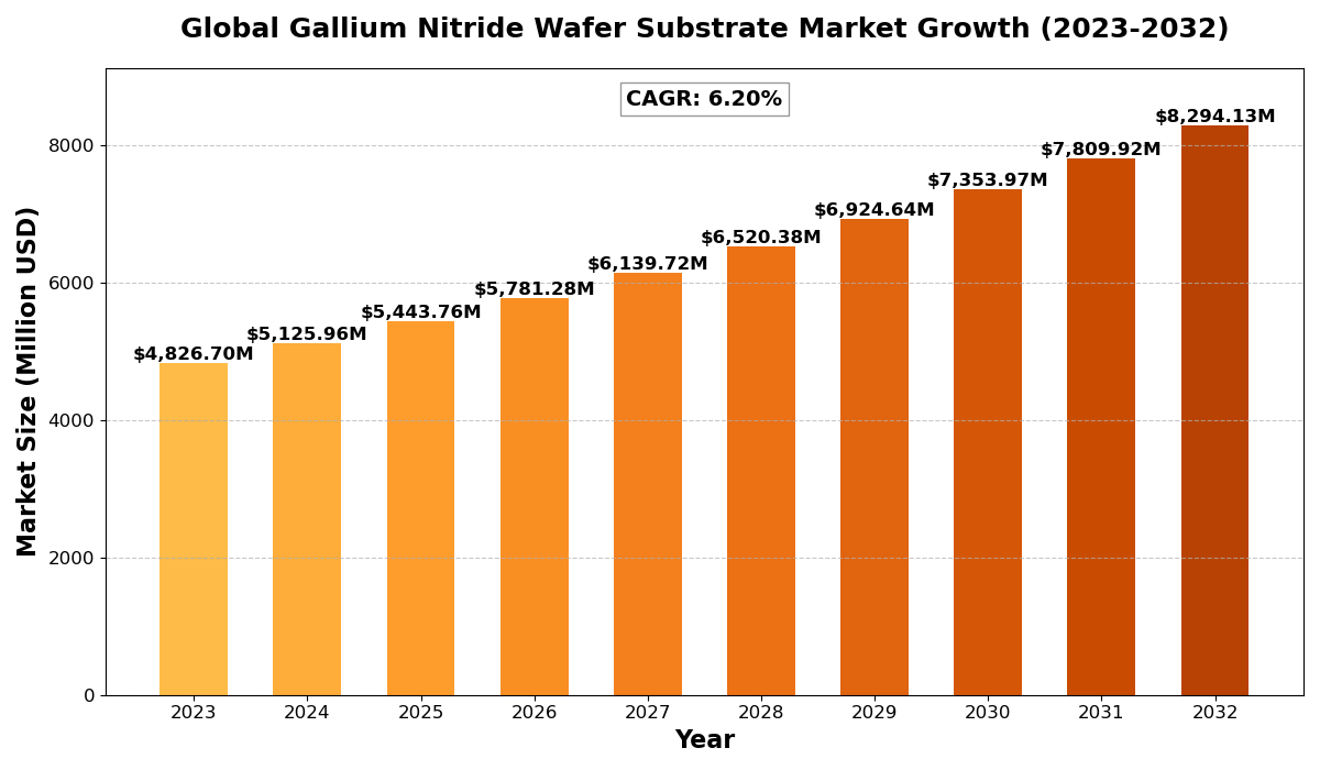
The global Gallium Nitride Wafer Substrate market size was estimated at USD 4826.70 million in 2023 and is projected to reach USD 8294.13 million by 2032, exhibiting a CAGR of 6.20% during the forecast period.
North America Gallium Nitride Wafer Substrate market size was estimated at USD 1394.93 million in 2023, at a CAGR of 5.31% during the forecast period of 2025 through 2032.
Gallium Nitride Wafer Substrate Key Market Trends :
- Rising Demand in Consumer Electronics
The increasing use of Gallium Nitride (GaN) wafers in smartphones, laptops, and other consumer electronics is driving market growth. - Expansion in Electric Vehicles (EVs)
GaN technology is gaining traction in the EV industry due to its high efficiency and power-saving capabilities. - Advancements in Semiconductor Manufacturing
Innovations in wafer processing and HVPE methods are improving the performance and cost-effectiveness of GaN substrates. - Growing Adoption in Aerospace & Defense
The high-power handling capability of GaN makes it a preferred choice for radar and satellite communication systems. - Increasing Investments in R&D
Major industry players are investing in research and development to enhance GaN wafer efficiency and reduce manufacturing costs.
Gallium Nitride Wafer Substrate Market Regional Analysis :

-
North America:
Strong demand driven by EVs, 5G infrastructure, and renewable energy, with the U.S. leading the market.
-
Europe:
Growth fueled by automotive electrification, renewable energy, and strong regulatory support, with Germany as a key player.
-
Asia-Pacific:
Dominates the market due to large-scale manufacturing in China and Japan, with growing demand from EVs, 5G, and semiconductors.
-
South America:
Emerging market, driven by renewable energy and EV adoption, with Brazil leading growth.
-
Middle East & Africa:
Gradual growth, mainly due to investments in renewable energy and EV infrastructure, with Saudi Arabia and UAE as key contributors.
Gallium Nitride Wafer Substrate Market Segmentation :
The research report includes specific segments by region (country), manufacturers, Type, and Application. Market segmentation creates subsets of a market based on product type, end-user or application, Geographic, and other factors. By understanding the market segments, the decision-maker can leverage this targeting in the product, sales, and marketing strategies. Market segments can power your product development cycles by informing how you create product offerings for different segments.
Key Company
- SCIOCS Corporation
- MSE Supplies
- Nitride Semiconductors Corporation
- Mitsubishi Chemical Corporation
- Powdec K K
- IQE
- Soitec Pte Ltd
- Fujitsu Limited
- NGK Insulators
- Infineon Technologies
- LumiGNtech
- American Elements
- Toshiba
- Koninklijke Philips
- Texas Instruments
- Saint Gobain
- Sumitomo Electric Industries
- Sino Nitride Semiconductors
- Xiamen Powerway Advanced Material
- Shanghai Famous Trade Corporation
Market Segmentation (by Type)
- 4-inch
- 6-inch
- 8-inch
- Others
Market Segmentation (by Application)
- Automobiles
- Consumer Electronics
- Defense and Aerospace
- Industrial Control
- Others
Market Drivers
- Increasing Demand for High-Performance Semiconductors
GaN wafers offer superior performance over silicon, making them essential in advanced semiconductor applications. - Growth of 5G Infrastructure
The expansion of 5G networks is boosting the demand for GaN-based RF components and power amplifiers. - Rising Need for Energy-Efficient Power Electronics
GaN wafers enhance power efficiency, making them crucial in electric vehicles, solar inverters, and industrial applications.
Market Restraints
- High Manufacturing Costs
The production process of GaN wafers is expensive, limiting their adoption in cost-sensitive markets. - Complex Fabrication Process
GaN wafer manufacturing requires advanced techniques, making scalability a challenge for new market entrants. - Competition from Silicon and Silicon Carbide (SiC)
Traditional silicon and SiC-based solutions still dominate some semiconductor applications due to lower costs.
Market Opportunities
- Expanding Role in Renewable Energy
GaN wafers are being increasingly used in solar power inverters and energy storage solutions. - Potential in Autonomous Vehicles
The use of GaN in LiDAR and power management systems is growing within the self-driving car industry. - Government Initiatives for Semiconductor Development
Various countries are investing in semiconductor manufacturing, creating growth opportunities for GaN wafer producers.
Market Challenges
- Supply Chain Disruptions
Shortages of raw materials and supply chain constraints can impact production and pricing. - Need for Technological Expertise
The specialized knowledge required for GaN wafer production limits the number of skilled professionals in the industry. - Regulatory and Environmental Concerns
Stringent regulations regarding semiconductor manufacturing could pose challenges to market expansion.
Key Benefits of This Market Research:
- Industry drivers, restraints, and opportunities covered in the study
- Neutral perspective on the market performance
- Recent industry trends and developments
- Competitive landscape & strategies of key players
- Potential & niche segments and regions exhibiting promising growth covered
- Historical, current, and projected market size, in terms of value
- In-depth analysis of the Gallium Nitride Wafer Substrate Market
- Overview of the regional outlook of the Gallium Nitride Wafer Substrate Market:
Key Reasons to Buy this Report:
- Access to date statistics compiled by our researchers. These provide you with historical and forecast data, which is analyzed to tell you why your market is set to change
- This enables you to anticipate market changes to remain ahead of your competitors
- You will be able to copy data from the Excel spreadsheet straight into your marketing plans, business presentations, or other strategic documents
- The concise analysis, clear graph, and table format will enable you to pinpoint the information you require quickly
- Provision of market value data for each segment and sub-segment
- Indicates the region and segment that is expected to witness the fastest growth as well as to dominate the market
- Provides insight into the market through Value Chain
- Market dynamics scenario, along with growth opportunities of the market in the years to come
- 6-month post-sales analyst support
Customization of the Report
In case of any queries or customization requirements, please connect with our sales team, who will ensure that your requirements are met.
FAQs
Q: What are the key driving factors and opportunities in the Gallium Nitride Wafer Substrate market?
A: The rising demand for high-performance semiconductors, 5G expansion, and energy-efficient electronics are key drivers. Opportunities include growth in renewable energy and autonomous vehicles.
Q: Which region is projected to have the largest market share?
A: The Asia-Pacific region, particularly China, Japan, and South Korea, is expected to dominate due to strong semiconductor manufacturing capabilities.
Q: Who are the top players in the global Gallium Nitride Wafer Substrate market?
A: Major companies include SCIOCS Corporation, Mitsubishi Chemical Corporation, Infineon Technologies, Sumitomo Electric Industries, and Texas Instruments.
Q: What are the latest technological advancements in the industry?
A: Advancements include improved HVPE methods, high-purity GaN substrates, and integration of GaN in power electronics and 5G infrastructure.
Q: What is the current size of the global Gallium Nitride Wafer Substrate market?
A: The market was valued at USD 4826.70 million in 2023 and is projected to reach USD 8294.13 million by 2032, with a CAGR of 6.20%.

Get Sample Report PDF for Exclusive Insights
Report Sample Includes
- Table of Contents
- List of Tables & Figures
- Charts, Research Methodology, and more...

