Flat No-leads Package Market Overview
Flat no-leads packages such as quad-flat no-leads (QFN) and dual-flat no-leads (DFN) physically and electrically connect integrated circuits to printed circuit boards. Flat no-leads, also known as micro leadframe (MLF) and SON (small-outline no leads), is a surface-mount technology, one of several package technologies that connect ICs to the surfaces of PCBs without through-holes.
This report provides a deep insight into the global Flat No-leads Package Market covering all its essential aspects. This ranges from a macro overview of the market to micro details of the market size, competitive landscape, development trend, niche market, key market drivers and challenges, SWOT analysis, value chain analysis, etc.
The analysis helps the reader to shape the competition within the industries and strategies for the competitive environment to enhance the potential profit. Furthermore, it provides a simple framework for evaluating and accessing the position of the business organization. The report structure also focuses on the competitive landscape of the Global Flat No-leads Package Market, this report introduces in detail the market share, market performance, product situation, operation situation, etc. of the main players, which helps the readers in the industry to identify the main competitors and deeply understand the competition pattern of the market.
In a word, this report is a must-read for industry players, investors, researchers, consultants, business strategists, and all those who have any kind of stake or are planning to foray into the Flat No-leads Package Market in any manner.
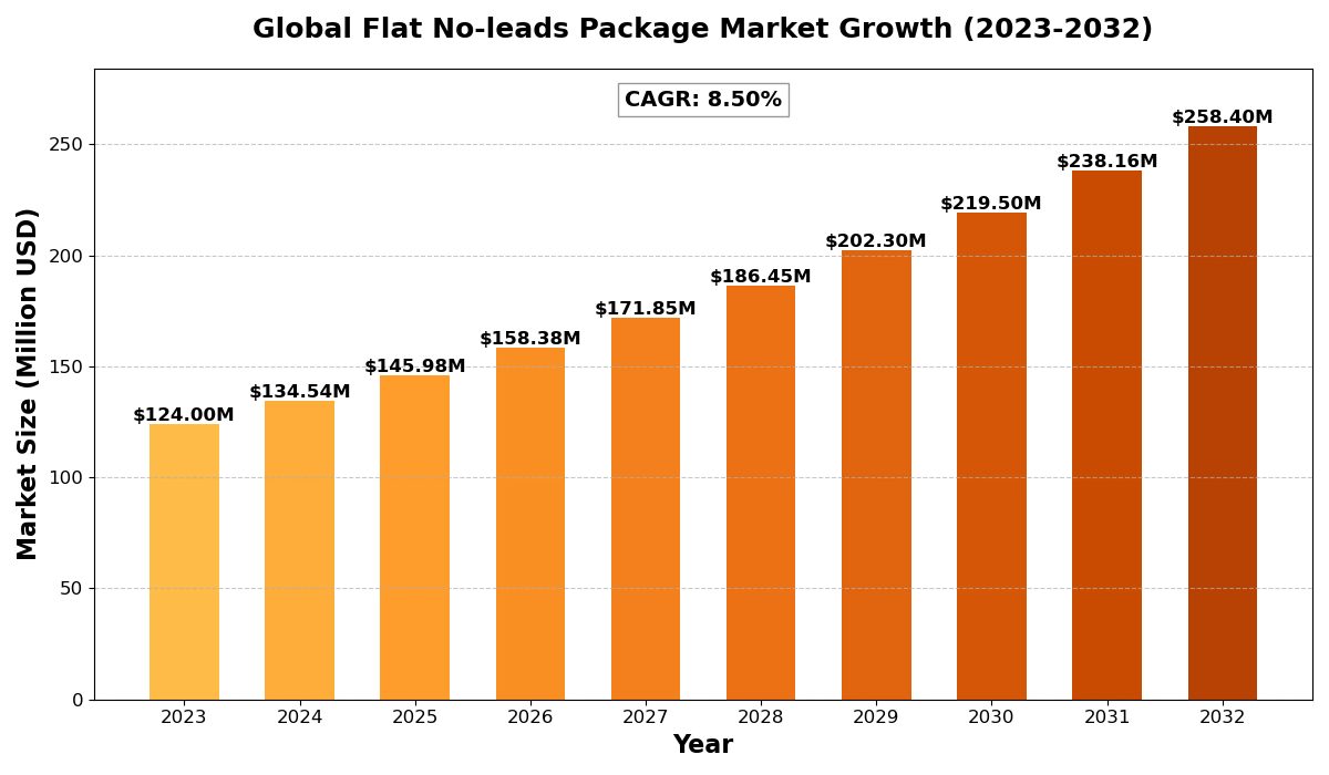
Flat No-leads Package Market Analysis:
The global Flat No-leads Package market size was estimated at USD 124 million in 2023 and is projected to reach USD 258.40 million by 2032, exhibiting a CAGR of 8.50% during the forecast period.
North America Flat No-leads Package market size was estimated at USD 37.19 million in 2023, at a CAGR of 7.29% during the forecast period of 2025 through 2032.
Flat No-leads Package Key Market Trends
The increasing demand for miniaturized electronic components is driving the adoption of flat no-leads (QFN, DFN) packages. These packages offer a compact footprint, better thermal performance, and improved electrical characteristics, making them ideal for high-density circuit designs.
The rise of 5G technology and IoT devices is fueling the market. As consumer electronics and industrial applications require faster data transmission and lower power consumption, flat no-leads packages are becoming a preferred choice for RF and power management applications.
Growing investments in advanced packaging technologies are shaping the market. Semiconductor manufacturers are focusing on enhancing QFN and DFN package designs by incorporating features such as wettable flanks for improved solderability and reliability in automotive and industrial applications.
The automotive industry’s shift toward electrification and ADAS (Advanced Driver Assistance Systems) is boosting demand. Flat no-leads packages are widely used in automotive electronics due to their high heat dissipation capabilities and compact design, supporting next-generation vehicle architectures.
Sustainability and cost-effectiveness are becoming key focus areas. Manufacturers are developing environmentally friendly packaging solutions with reduced material usage while maintaining high performance, aligning with global sustainability initiatives.
Flat No-leads Package Market Regional Analysis :

- North America:Strong demand driven by EVs, 5G infrastructure, and renewable energy, with the U.S. leading the market.
- Europe:Growth fueled by automotive electrification, renewable energy, and strong regulatory support, with Germany as a key player.
- Asia-Pacific:Dominates the market due to large-scale manufacturing in China and Japan, with growing demand from EVs, 5G, and semiconductors.
- South America:Emerging market, driven by renewable energy and EV adoption, with Brazil leading growth.
- Middle East & Africa:Gradual growth, mainly due to investments in renewable energy and EV infrastructure, with Saudi Arabia and UAE as key contributors.
Flat No-leads Package Market Segmentation
The research report includes specific segments by region (country), manufacturers, Type, and Application. Market segmentation creates subsets of a market based on product type, end-user or application, Geographic, and other factors. By understanding the market segments, the decision-maker can leverage this targeting in the product, sales, and marketing strategies. Market segments can power your product development cycles by informing how you create product offerings for different segments.
Key Company
- Amkor Technology
- SFA Semicon
- Advanced Dicing Technologies
- DISCO
- ASE
- Orient Semiconductor Electronics
- King Yuan Electronics
- JCET
- Suzhou Si-Era
- Nantong Jiejing
- Ningbo ChipEx Semiconductor
Market Segmentation (by Type)
- Air-cavity QFNs
- Plastic-moulded QFNs
Market Segmentation (by Application)
- Consumer Electronics
- Automotive
- Medical
- Telecommunication
- Others
Drivers
The increasing need for high-performance, space-saving semiconductor solutions is a major driver. Flat no-leads packages provide excellent thermal and electrical performance, making them ideal for compact and power-efficient electronic devices.
The expanding consumer electronics and telecommunications sectors are driving market growth. The widespread adoption of smartphones, wearables, and wireless communication modules is boosting demand for flat no-leads packages in integrated circuits.
Rising automation and industrial IoT applications are fueling demand. Industrial equipment and smart factory systems require robust and reliable packaging solutions for embedded processors, sensors, and power management ICs.
Restraints
Manufacturing complexity and yield issues pose a challenge. The production of flat no-leads packages requires precise assembly and inspection techniques, leading to potential defects that can impact overall yield rates.
High initial costs for advanced packaging equipment are limiting adoption. Semiconductor manufacturers must invest in specialized tools and processes, which can be costly for smaller industry players.
The risk of thermal management issues in high-power applications remains a concern. While flat no-leads packages offer good heat dissipation, excessive heat buildup in high-power devices can impact performance and reliability.
Opportunities
The development of next-generation semiconductor materials is creating new growth avenues. Innovations such as gallium nitride (GaN) and silicon carbide (SiC) in power electronics are expanding the use of flat no-leads packages in high-efficiency applications.
Expanding applications in medical and aerospace electronics are driving demand. The need for compact, lightweight, and high-reliability components is pushing the adoption of advanced packaging solutions in critical industries.
Increased adoption of automation and AI-driven manufacturing processes is improving production efficiency. Semiconductor companies are leveraging AI-based inspection and defect detection systems to enhance yield rates and reduce manufacturing costs.
Challenges
Maintaining high reliability and durability in harsh environments is a significant challenge. Automotive, aerospace, and industrial applications require packaging solutions that can withstand extreme temperatures, vibrations, and moisture exposure.
Compliance with stringent regulatory standards is essential. Flat no-leads packages used in medical and automotive applications must meet strict quality and safety requirements, increasing production complexity.
Fluctuations in semiconductor supply chains impact market stability. Geopolitical issues, raw material shortages, and production disruptions can affect the availability and pricing of flat no-leads packages.
Key Benefits of This Market Research:
- Industry drivers, restraints, and opportunities covered in the study
- Neutral perspective on the market performance
- Recent industry trends and developments
- Competitive landscape & strategies of key players
- Potential & niche segments and regions exhibiting promising growth covered
- Historical, current, and projected market size, in terms of value
- In-depth analysis of the Flat No-leads Package Market
- Overview of the regional outlook of the Flat No-leads Package Market:
Key Reasons to Buy this Report:
- Access to date statistics compiled by our researchers. These provide you with historical and forecast data, which is analyzed to tell you why your market is set to change
- This enables you to anticipate market changes to remain ahead of your competitors
- You will be able to copy data from the Excel spreadsheet straight into your marketing plans, business presentations, or other strategic documents
- The concise analysis, clear graph, and table format will enable you to pinpoint the information you require quickly
- Provision of market value data for each segment and sub-segment
- Indicates the region and segment that is expected to witness the fastest growth as well as to dominate the market
- Provides insight into the market through Value Chain
- Market dynamics scenario, along with growth opportunities of the market in the years to come
- 6-month post-sales analyst support
Customization of the Report
In case of any queries or customization requirements, please connect with our sales team, who will ensure that your requirements are met.
FAQs
Q: What are the key driving factors and opportunities in the Flat No-leads Package market?
A: The demand for miniaturized, high-performance semiconductor solutions is driving market growth. Opportunities exist in advanced packaging materials, automotive electronics, and AI-driven manufacturing.
Q: Which region is projected to have the largest market share?
A: Asia-Pacific is expected to dominate due to its strong semiconductor manufacturing base in China, Taiwan, and South Korea, along with increasing demand for consumer electronics and automotive applications.
Q: Who are the top players in the global Flat No-leads Package market?
A: Leading companies include Texas Instruments, NXP Semiconductors, ON Semiconductor, Amkor Technology, and ASE Group, focusing on advanced packaging solutions for various industries.
Q: What are the latest technological advancements in the industry?
A: Innovations include wettable flank technology for better soldering, GaN and SiC-based packaging for power applications, and AI-driven quality control in semiconductor packaging.
Q: What is the current size of the global Flat No-leads Package market?
A: The market is expected to grow significantly from 2025 to 2032, driven by rising demand for compact and efficient semiconductor packaging solutions across multiple industries.

Get Sample Report PDF for Exclusive Insights
Report Sample Includes
- Table of Contents
- List of Tables & Figures
- Charts, Research Methodology, and more...