
Market Insights
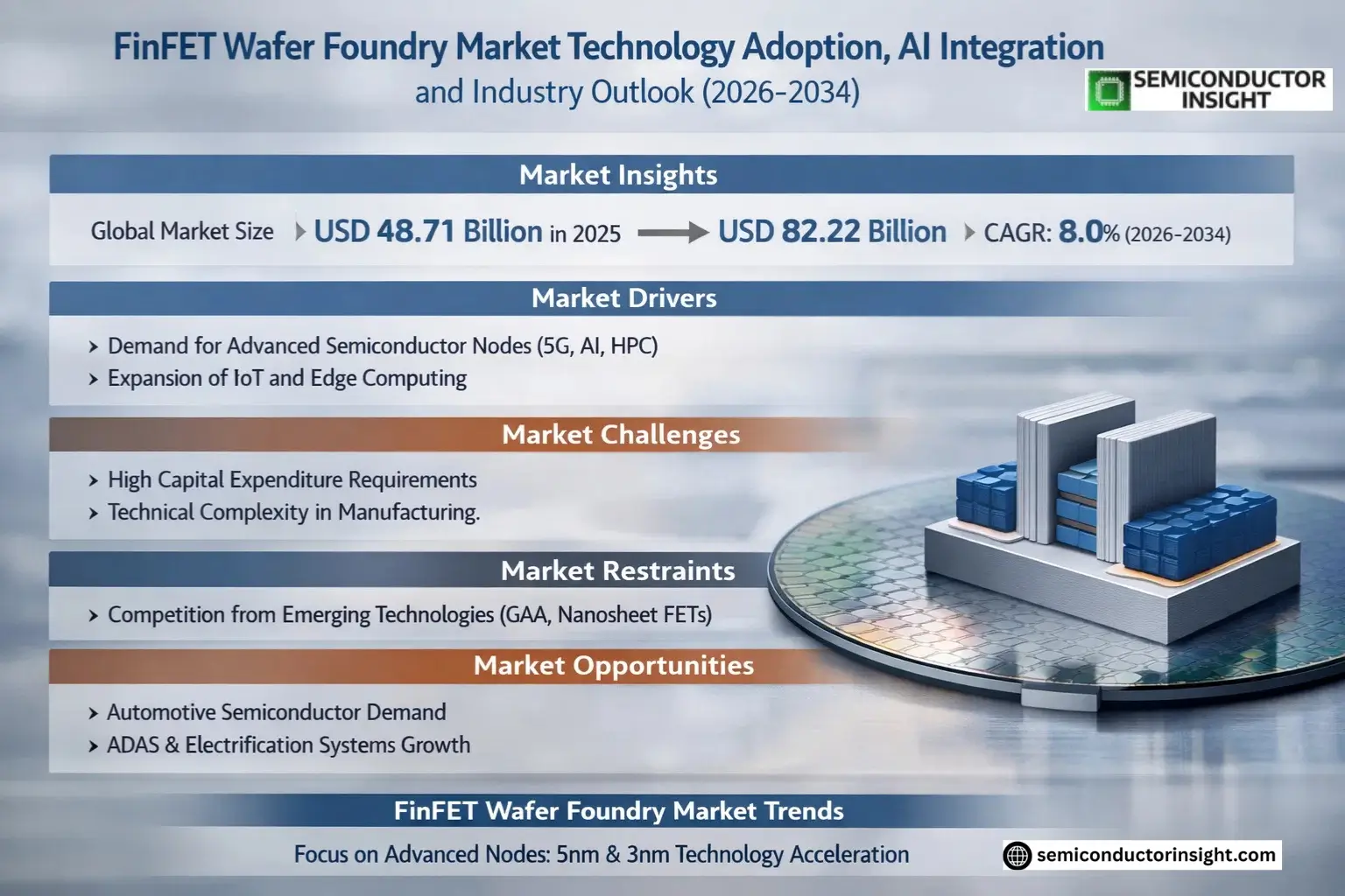
Global FinFET Wafer Foundry Market size was valued at USD 48.71 billion in 2025. The market is projected to grow from USD 52.6 billion in 2026 to USD 82.22 billion by 2034, exhibiting a CAGR of 8.0% during the forecast period.
A FinFET (Fin Field-Effect Transistor) is an advanced semiconductor device architecture featuring three-dimensional fins that enable superior electrostatic control compared to traditional planar transistors. These vertically stacked silicon fins allow for higher performance, lower power consumption, and reduced current leakage – making them ideal for cutting-edge applications like high-performance computing and mobile processors.
The market growth is primarily driven by increasing demand for energy-efficient chips across smartphones, IoT devices, and data centers. While TSMC currently dominates production with over 50% market share, competitors like Samsung Foundry and Intel are aggressively expanding their FinFET capacity through multi-billion-dollar fab investments. Recent technological breakthroughs in extreme ultraviolet (EUV) lithography have further accelerated the adoption of sub-7nm FinFET nodes across the industry.
MARKET DRIVERS
Growing Demand for Advanced Semiconductor Nodes
FinFET Wafer Foundry Market is experiencing significant growth due to rising demand for advanced semiconductor nodes in 5G, AI, and high-performance computing applications. Leading foundries are investing heavily in FinFET technology to meet the needs of cutting-edge chip designs. The technology’s superior power efficiency and performance make it ideal for next-generation devices.
Expansion of IoT and Edge Computing
With the rapid expansion of IoT devices and edge computing solutions, FinFET wafer foundries are seeing increased demand for low-power, high-performance chips. The technology’s ability to deliver better leakage control at smaller nodes is driving adoption across automotive, industrial, and consumer electronics sectors.
Continuous miniaturization of semiconductor components is further accelerating the transition to FinFET technology across multiple application segments.
MARKET CHALLENGES
High Capital Expenditure Requirements
FinFET Wafer Foundry Market faces significant barriers due to the enormous capital investments required for fabrication facilities. Building and maintaining FinFET production lines costs billions of dollars, limiting market entry to only the largest semiconductor companies.
Other Challenges
Technical Complexity in Manufacturing
FinFET production involves complex process steps and stringent quality control requirements, leading to lower yields compared to planar technologies during initial production phases.
MARKET RESTRAINTS
Competition from Alternative Technologies
FinFET Wafer Foundry Market faces competition from emerging technologies like gate-all-around (GAA) transistors and nanosheet FETs. As these alternatives mature, they may divert investment from FinFET production in the long term. However, FinFET remains the dominant technology for nodes between 7nm and 22nm.
MARKET OPPORTUNITIES
Automotive Semiconductor Demand Surge
The automotive industry’s growing need for advanced chips in ADAS, infotainment, and electrification systems presents significant opportunities for FinFET wafer foundries. The technology’s reliability and performance characteristics align well with automotive-grade requirements, opening new revenue streams for foundry providers.
FinFET Wafer Foundry Market Trends
Acceleration of Advanced Node Adoption
FinFET Wafer Foundry Market is witnessing accelerated adoption of advanced process nodes, particularly 5nm and 3nm technologies. Leading manufacturers are prioritizing these nodes for high-performance computing and smartphone applications. Foundries investing in capacity expansion for 3nm FinFET production are gaining competitive advantage as demand increases for next-gen semiconductor devices.
Other Trends
Regional Capacity Expansion
Significant investments are being made in new fabrication facilities across Taiwan, South Korea, and the United States. The geopolitical landscape is influencing regional diversification strategies, with governments supporting domestic semiconductor manufacturing capabilities to ensure supply chain resilience.
Competitive Landscape Shifts
The market remains dominated by TSMC, but competitors are narrowing the technology gap through strategic partnerships and R&D investments. Samsung Foundry and Intel Foundry Services are making substantial progress in advanced FinFET nodes, challenging the current market hierarchy while maintaining quality and yield standards.
Application-Specific Innovation
Foundries are developing specialized FinFET solutions for automotive and IoT applications, where reliability and power efficiency are critical. This includes modified process flows and design rule optimizations to meet stringent requirements for these growing market segments.
Material and Architecture Advancements
Research continues into new channel materials and gate stack engineering to extend FinFET roadmap viability beyond 3nm nodes. While alternative architectures are emerging, FinFET technology remains the production-proven choice for most foundry customers through at least the next product generation cycle.
COMPETITIVE LANDSCAPE
Key Industry Players
Global FinFET Wafer Foundry Market Dominated by Few Advanced Semiconductor Manufacturers
Taiwan Semiconductor Manufacturing Company (TSMC) leads the FinFET Wafer Foundry Market with over 60% market share in advanced nodes (7nm and below). Their technological leadership in 3nm and upcoming 2nm processes creates significant barriers to entry. Samsung Foundry emerges as the closest competitor with its Gate-All-Around (GAA) technology at 3nm, capturing nearly 20% of the advanced foundry business. The market demonstrates an oligopolistic structure where only six companies currently offer FinFET manufacturing below 16nm.
While TSMC and Samsung dominate cutting-edge nodes, GlobalFoundries maintains strong presence in 12nm/14nm FinFET for automotive and IoT applications. Chinese players like SMIC are rapidly advancing, though currently limited to 14nm production due to export restrictions. Intel Foundry Services represents the newest entrant with aggressive roadmap to challenge TSMC’s leadership by 2025. Specialty foundries like UMC focus on cost-optimized FinFET solutions for non-leading-edge applications.
List of Key FinFET Wafer Foundry Companies Profiled
- Taiwan Semiconductor Manufacturing Company (TSMC)
- Samsung Foundry
- GlobalFoundries
- United Microelectronics Corporation (UMC)
- Semiconductor Manufacturing International Corporation (SMIC)
- Intel Foundry Services (IFS)
- Tower Semiconductor
- Powerchip Semiconductor Manufacturing Corporation
- Vanguard International Semiconductor Corporation
- Shanghai Huali Microelectronics Corporation (HLMC)
- Nexchip Semiconductor Corporation
- DB HiTek
- Key Foundry
- X-FAB Silicon Foundries
- Dongbu HiTek
Segment Analysis:
| Segment Category | Sub-Segments | Key Insights |
| By Type |
|
5nm FinFET dominates with superior balance between performance and power efficiency.
|
| By Application |
|
Smartphone applications represent the largest market segment for FinFET wafers.
|
| By End User |
|
Fabless semiconductor companies are the primary consumers of FinFET foundry services.
|
| By Technology Node |
|
Leading-edge nodes demonstrate strongest growth momentum in the market.
|
| By Geography |
|
Asia Pacific maintains leadership due to concentrated semiconductor ecosystem.
|
Regional Analysis: FinFET Wafer Foundry Market
Taiwan maintains its position as the global FinFET hub through TSMC’s continuous node advancement and massive R&D investments. The foundry’s 5nm and upcoming 3nm FinFET processes cater to high-performance computing demands from Apple, AMD, and Nvidia.
Samsung leverages its FinFET technology for advanced DRAM and NAND flash memory integration, creating synergies between logic and memory in AI applications. Their gate-all-around (GAA) transition builds upon FinFET foundations for next-gen chips.
Chinese foundries like SMIC are rapidly catching up with 14nm FinFET production despite export controls. Government initiatives aim to achieve self-sufficiency in semiconductor manufacturing through massive funding of domestic FinFET development.
The Asia-Pacific benefits from complete semiconductor ecosystems including materials suppliers, packaging houses, and testing facilities clustered around major foundries. This integrated infrastructure enables faster time-to-market for FinFET-based products.
North America
North America remains a key player in FinFET wafer technology through design leadership and advanced R&D. While lacking major pure-play foundries, the region hosts Intel’s IDM operations transitioning to FinFET architectures. The U.S. CHIPS Act aims to revitalize domestic manufacturing capabilities with incentives for FinFET-based foundries. Major fabless companies like Qualcomm and Apple drive demand for cutting-edge FinFET wafers from Asian foundries. Research institutions collaborate with industry on next-generation FinFET applications in AI accelerators and quantum computing.
Europe
Europe maintains strategic positions in specialty FinFET applications through companies like STMicroelectronics and Infineon. The region focuses on automotive and industrial applications where reliability outweighs leading-edge node requirements. EU initiatives aim to double semiconductor market share with investments in FD-SOI and FinFET hybrid technologies. Collaborative research programs between universities and manufacturers explore energy-efficient FinFET designs for IoT and edge computing devices.
Middle East & Africa
The Middle East is emerging as a potential FinFET manufacturing hub with Saudi Arabia and UAE investing in semiconductor infrastructure. While currently lacking advanced nodes, the region offers strategic advantages in energy costs and geopolitical stability. African nations are establishing basic semiconductor packaging and testing capabilities that could integrate with global FinFET supply chains in coming years.
South America
South America’s semiconductor market remains focused on assembly and testing rather than advanced manufacturing. Brazil has nascent efforts in semiconductor research with potential to develop specialty FinFET applications for agricultural tech and energy. The region serves primarily as a consumer market for FinFET-based electronics with growing demand in telecommunications infrastructure.
Report Scope
This market research report provides a comprehensive analysis of the FinFET Wafer Foundry Market, covering the forecast period 2025–2034. It offers detailed insights into market dynamics, technological advancements, competitive landscape, and key trends shaping the industry.
Key focus areas of the report include:
- Market Overview: The report begins with an overview outlining its current market scenario, key growth indicators, and industry transformation drivers. It discusses macroeconomic factors, demand–supply balance, regulatory landscape, and the strategic role of semiconductors in powering advancements across industries such as automotive, telecommunications, consumer electronics, and industrial automation.
- Market Size & Forecast: Historical data and future projections for revenue, unit shipments, and market value across major regions and segments.
- Segmentation Analysis: Detailed breakdown by product type, technology, application, and end-user industry to identify high-growth segments and investment opportunities.
- Regional Insights: Insights into market performance across North America, Europe, Asia-Pacific, Latin America, and the Middle East & Africa, including country-level analysis where relevant.
- Competitive Landscape: Profiles of leading market participants, including their product offerings, R&D focus, manufacturing capacity, pricing strategies, and recent developments such as mergers, acquisitions, and partnerships.
- Technology Trends & Innovation: Assessment of emerging technologies, integration of AI/IoT, semiconductor design trends, fabrication techniques, and evolving industry standards.
- Market Drivers & Restraints: Evaluation of factors driving market growth along with challenges, supply chain constraints, regulatory issues, and market-entry barriers.
- Stakeholder Insights: Insights for component suppliers, OEMs, system integrators, investors, and policymakers regarding the evolving ecosystem and strategic opportunities.
Primary and secondary research methods are employed, including interviews with industry experts, data from verified sources, and real-time market intelligence to ensure the accuracy and reliability of the insights presented.
FREQUENTLY ASKED QUESTIONS:
What is the current market size of FinFET Wafer Foundry Market?
-> FinFET Wafer Foundry Market size was valued at USD 48.71 billion in 2025. The market is projected to grow from USD 52.6 billion in 2026 to USD 82.22 billion by 2034, exhibiting a CAGR of 8.0% during the forecast period.
What is the growth rate (CAGR) of the FinFET Wafer Foundry Market?
-> The market is expected to grow at a CAGR of 8.0% during the forecast period 2025-2034.
Which key companies operate in FinFET Wafer Foundry Market?
-> Key players include TSMC, Samsung Foundry, GlobalFoundries, United Microelectronics Corporation (UMC), SMIC, and Intel Foundry Services (IFS).
What are the key application areas for FinFET Wafer Foundry?
-> Major applications include High Performance Computing (HPC), Smartphones, Wearable and IoT Devices, Automotive, and others.
Which regions are leading in FinFET Wafer Foundry Market?
-> Asia-Pacific dominates the market, with significant contributions from China, Japan, and South Korea.
What are the key process platforms in FinFET Wafer Foundry Market?
-> Major process platforms include 3nm FinFET, 5nm FinFET, 7/10nm FinFET, and 14/16nm FinFET.
Get Sample Report PDF for Exclusive Insights
Report Sample Includes
- Table of Contents
- List of Tables & Figures
- Charts, Research Methodology, and more...
 Download Sample Report PDF