MARKET INSIGHTS
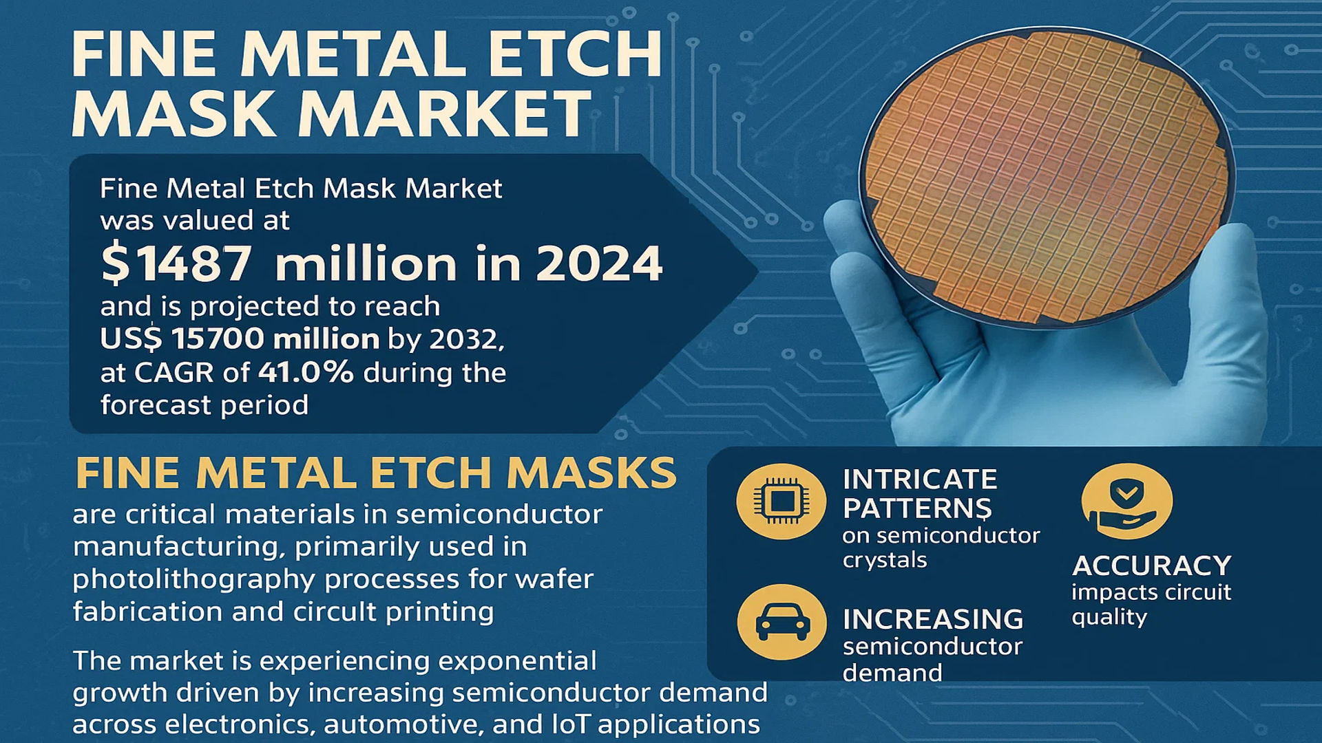
The global Fine Metal Etch Mask Market was valued at 1487 million in 2024 and is projected to reach US$ 15700 million by 2032, at a CAGR of 41.0% during the forecast period.
Fine Metal Etch Masks are critical materials in semiconductor manufacturing, primarily used in photolithography processes for wafer fabrication and circuit printing. These precision masks enable the creation of intricate patterns on semiconductor crystals, facilitating processes like doping window formation, electrode contact hole etching, and metal interconnection patterning. Their accuracy directly impacts circuit quality and end-product performance.
The market is experiencing exponential growth driven by increasing semiconductor demand across electronics, automotive, and IoT applications. While production is currently dominated by US, Japanese, and European manufacturers, technological advancements are creating opportunities for emerging players. The market witnessed record growth in 2022 with USD 878.2 million in sales, reflecting the strong correlation between semiconductor material innovation and electronic device miniaturization trends.
MARKET DYNAMICS
MARKET DRIVERS
Expanding Semiconductor Industry to Propel Demand for Fine Metal Etch Masks
The global semiconductor industry has been experiencing robust growth, with annual revenues surpassing $600 billion, creating substantial demand for fine metal etch masks. These masks are critical components in semiconductor manufacturing, particularly for advanced nodes below 10nm where precision etching becomes increasingly important. As chipmakers continue to push the boundaries of miniaturization, the need for high-quality etch masks with sub-micron resolution has surged. The market is further driven by rising investments in fabrication facilities worldwide, with over $150 billion expected to be invested in new semiconductor plants by 2025.
Growing Adoption of Advanced Packaging Technologies Boosts Market Growth
The shift towards heterogeneous integration and 3D packaging solutions has created new opportunities for fine metal etch mask manufacturers. Advanced packaging technologies such as fan-out wafer-level packaging (FoWLP) and 3D IC stacking require specialized etch masks with precise pattern transfer capabilities. These technologies are becoming increasingly important as the industry moves beyond Moore’s Law, with the advanced packaging market projected to grow at a compound annual rate of over 10% through 2030. The complexity of these packaging solutions often requires multiple etch mask layers, further driving market expansion.
Increasing Demand for Consumer Electronics Accelerates Market Expansion
The proliferation of smartphones, tablets, and other smart devices continues to fuel demand for semiconductor components that rely on fine metal etch mask technology. With over 1.5 billion smartphones shipped annually and the rapid adoption of 5G technology driving component upgrades, semiconductor manufacturers are under constant pressure to increase production capacity. This has led to significant capital expenditures in semiconductor equipment, including etch mask technology, with the foundry sector alone investing more than $50 billion annually in capacity expansion and technology upgrades.
MARKET RESTRAINTS
High Cost of Advanced Etch Mask Technologies Limits Market Penetration
The development and production of high-end fine metal etch masks involve substantial capital investment and technical expertise, creating barriers to entry for smaller manufacturers. The equipment required for producing masks with nanometer-scale precision can cost tens of millions of dollars, while the development of new mask materials and processes requires significant R&D expenditures. These high costs are particularly challenging for emerging markets and smaller semiconductor producers, potentially limiting market growth in price-sensitive segments.
Technical Challenges in Extreme Ultraviolet (EUV) Mask Production Constrain Capacity
As semiconductor manufacturing transitions to EUV lithography, the production of EUV-compatible etch masks presents significant technical hurdles. EUV masks require unprecedented levels of defect control and flatness, with acceptable defect densities below 0.01 per square centimeter. This extreme quality requirement has led to yield challenges in mask production, with only a handful of facilities worldwide capable of manufacturing EUV masks at volume. The resulting supply constraints could potentially slow the adoption of next-generation semiconductor nodes.
Stringent Environmental Regulations Impact Production Processes
The chemicals and processes used in etch mask production are increasingly subject to environmental regulations that add complexity and cost to manufacturing operations. Many traditional etchants and cleaning solutions are being phased out due to environmental concerns, requiring substantial investments in alternative chemistries and process development. Compliance with evolving regulations in different geographic markets adds another layer of complexity for global manufacturers, potentially impacting production efficiency and time-to-market.
MARKET OPPORTUNITIES
Emerging Applications in Photonics and MEMS Create New Growth Avenues
Beyond traditional semiconductor applications, fine metal etch masks are finding growing use in photonic integrated circuits and micro-electromechanical systems (MEMS). The photonics market is expanding rapidly, with applications in data communications, sensing, and quantum computing. MEMS devices, used in everything from automotive sensors to medical devices, require specialized etch patterns that benefit from advanced mask technology. These emerging applications represent significant growth opportunities as they often command higher margins than conventional semiconductor markets.
Geographic Expansion of Semiconductor Manufacturing Boosts Regional Demand
The establishment of new semiconductor manufacturing hubs in regions such as Southeast Asia and North America presents significant opportunities for etch mask suppliers. Government initiatives supporting domestic semiconductor production, such as the CHIPS Act in the United States, are driving billions of dollars in new fabrication facility investments. These developments create fresh demand for etch mask technologies while also encouraging localization of supply chains, offering growth prospects for both established players and new entrants in these regions.
Advancements in Maskless Lithography Enable New Business Models
Emerging maskless lithography technologies present opportunities for innovative approaches to pattern transfer. While still in development for high-volume manufacturing, these technologies could complement traditional etch masks by enabling rapid prototyping and small-lot production. Companies that can position themselves at the intersection of conventional mask technology and these new approaches stand to benefit from the growing need for flexible manufacturing solutions to support research, development, and low-volume specialty production.
MARKET CHALLENGES
Complex Supply Chain Dynamics Create Operational Challenges
The fine metal etch mask market operates within a complex global supply chain that has proven vulnerable to disruptions. The highly specialized nature of mask production means that most facilities rely on a limited number of suppliers for critical materials and equipment. Recent semiconductor industry shortages have highlighted the risks of this concentration, with lead times for certain mask production tools extending beyond 12 months. These challenges are compounded by geopolitical factors that can impact the flow of materials and technology across borders.
Rapid Technological Evolution Requires Continuous R&D Investment
The accelerating pace of semiconductor technology development creates significant challenges for etch mask manufacturers. Each new process node typically requires innovations in mask materials, dimensional control, and inspection methodologies. Keeping pace with these developments demands continuous R&D investment, which can be particularly challenging for smaller players. The transition to gate-all-around transistors and other advanced device architectures will require new mask solutions, potentially disrupting existing technologies and business models.
Intellectual Property Protection Concerns in Global Markets
As more semiconductor manufacturing capacity moves to emerging markets, intellectual property protection remains a significant challenge for etch mask technology developers. The high value and technical sophistication of advanced mask technologies make them particularly vulnerable to unauthorized replication. Establishing operations in certain regions while adequately protecting proprietary technologies requires careful navigation of complex legal and business environments, potentially limiting market expansion opportunities in some geographies.
FINE METAL ETCH MASK MARKET TRENDS
Rising Semiconductor Demand Fueling the Fine Metal Etch Mask Market
The global semiconductor industry continues to expand at an unprecedented rate, with fine metal etch masks playing a critical role in semiconductor lithography. These masks enable the precise etching of metal layers during chip fabrication, directly impacting the quality and efficiency of integrated circuits. With the global market valued at $1.487 billion in 2024 and projected to reach $15.7 billion by 2032, the sector is experiencing exponential growth, supported by the increasing demand for advanced electronics, AI-driven computing, and IoT applications. The Asia-Pacific region, particularly China, Japan, and South Korea, dominates the market, accounting for over 60% of global production due to strong semiconductor manufacturing capabilities.
Other Trends
Technological Advancements in Lithography
The shift toward smaller nodes in semiconductor manufacturing, particularly below 5nm and 3nm, has intensified the need for high-precision fine metal etch masks. Innovations such as extreme ultraviolet (EUV) lithography are reshaping the industry, as traditional photolithography struggles to maintain precision at reduced feature sizes. The adoption of multi-material composite masks has surged, as they offer superior resistance to etching chemicals while maintaining the required resolution for cutting-edge chip designs. Additionally, manufacturers are increasingly leveraging AI-assisted mask design to optimize patterning and defect minimization.
Supply Chain Diversification and Regional Shifts
Geopolitical tensions and supply chain vulnerabilities have prompted semiconductor manufacturers to diversify their fine metal etch mask sourcing strategies. While the U.S., Japan, and Europe lead in technology and supply, emerging players in China are making significant R&D investments to reduce dependency on foreign suppliers. For instance, Chinese manufacturers have recently achieved breakthroughs in mask precision and yield rates, though they still lag behind global leaders in consistency and large-scale production efficiency. Meanwhile, collaborations between mask suppliers and semiconductor fabricators are increasing to ensure seamless integration of next-generation etching solutions.
COMPETITIVE LANDSCAPE
Key Industry Players
Semiconductor Giants and Niche Specialists Compete in Evolving Fine Metal Etch Mask Market
The global Fine Metal Etch Mask market exhibits a dynamic competitive environment where established semiconductor material suppliers compete with specialized manufacturers. Dai Nippon Printing (DNP) and Toppan Printing Co., Ltd. currently dominate the market, collectively holding approximately 32% of the global revenue share in 2024. These Japanese corporations benefit from decades of experience in precision lithography solutions and maintain strategic partnerships with leading semiconductor foundries.
While the market remains concentrated among top players, emerging competitors like V-TECHNOLOGY CO., LTD. are gaining traction through technological differentiation. V-TECHNOLOGY’s proprietary multi-layer etch mask technology, which reduces pattern distortion by 18% compared to conventional methods according to recent performance benchmarks, exemplifies this trend. Meanwhile, Korean firm Poongwon has strengthened its position through aggressive pricing strategies and localized supply chains serving the growing Asian semiconductor ecosystem.
The competitive landscape is further shaped by vertical integration strategies. Companies such as Etch Tech have expanded beyond mask production to offer complete patterning solutions, including etcher equipment and process optimization services. This approach helps lock in customers across the semiconductor manufacturing value chain. Conversely, pure-play mask specialists like APS Holding focus on high-margin, application-specific designs for advanced packaging and MEMS applications.
Recent industry developments underscore the intensifying competition:
- DNP’s 2023 acquisition of a German photomask specialist expanded its EUV lithography capabilities
- Toppan’s strategic investment in AI-driven mask inspection systems reduced defect rates by 23% in pilot production
- Lianchuang Optoelectronics securing design wins with three major Chinese semiconductor manufacturers
List of Key Fine Metal Etch Mask Companies Profiled
- Dai Nippon Printing (DNP) (Japan)
- Toppan Printing Co., Ltd (Japan)
- DNP Group (Japan)
- V-TECHNOLOGY CO., LTD. (Japan)
- Poongwon (South Korea)
- APS Holding (U.S.)
- Etch Tech (U.S.)
- Atehene (Germany)
- Lianchuang Optoelectronics (China)
- Shandong Aolai Electronic Technology Co., Ltd. (China)
Segment Analysis:
By Type
Etching Segment Drives Market Growth Owing to High Precision in Semiconductor Manufacturing
The market is segmented based on type into:
- Etching
- Electroforming
- Multi-material Composite Method
By Application
Semiconductor Manufacturing Leads Due to Increasing Demand for Advanced Chips
The market is segmented based on application into:
- Semiconductor manufacturing
- Photonic crystals
- LCD TV
- Cell phone
- Computer
- Flat panel displays
- Others
By End-User
Foundries Account for Significant Demand Due to High-Volume Production Requirements
The market is segmented based on end-user into:
- Semiconductor foundries
- IDMs (Integrated Device Manufacturers)
- Research institutions
- Electronics manufacturers
Regional Analysis: Fine Metal Etch Mask Market
Asia-Pacific
Asia-Pacific dominates the global fine metal etch mask market, accounting for the largest revenue share due to the region’s robust semiconductor manufacturing ecosystem. Countries like China, Japan, and South Korea lead in production and consumption, supported by extensive electronics manufacturing and strong government investments in semiconductor self-sufficiency. China’s push to strengthen domestic semiconductor capabilities under initiatives like the National Integrated Circuit Industry Development Guidelines is driving significant demand. Japan remains a technological leader, with companies like Toppan Printing and Dai Nippon Printing commanding substantial market shares. While cost-competitive manufacturing drives adoption, stricter environmental regulations are gradually shifting preferences toward advanced, low-defect etch masks.
North America
The North American market thrives on cutting-edge semiconductor R&D and high-volume chip production, particularly in the U.S. Companies such as Intel and GlobalFoundries rely on precision etch masks for advanced nodes below 7nm, fueling demand from suppliers like Etch Tech. The CHIPS and Science Act, allocating $52 billion for semiconductor manufacturing and research, is accelerating fab expansions and technological advancements. However, reliance on Asian suppliers for certain mask types poses supply chain challenges. Regulatory emphasis on semiconductor sovereignty is prompting strategic partnerships between domestic and international manufacturers to bolster supply reliability.
Europe
Europe’s market is characterized by specialized demand for high-performance etch masks, particularly in photonics and automotive semiconductor applications. The region benefits from strong collaboration between research institutions and manufacturers, such as Germany’s Fraunhofer Institute and ASML’s lithography advancements. EU policies like the European Chips Act, which earmarks €43 billion for semiconductor autonomy, are driving investments in mask fabrication. However, the market faces constraints due to limited local production capacity, with reliance on imports from Asia and the U.S. for advanced-node masks.
South America
The South American market remains nascent but shows potential due to growing electronics assembly activities, particularly in Brazil and Mexico. Most demand stems from consumer electronics manufacturing, though adoption of advanced etch masks is hindered by economic volatility and limited local semiconductor fabrication. The absence of domestic mask suppliers further necessitates imports, slowing technical progress. Nevertheless, increasing foreign investments in regional electronics production could create opportunities for market growth over the long term.
Middle East & Africa
This region exhibits marginal but emerging demand, primarily led by limited wafer fabrication and packaging facilities in Israel and UAE. High dependency on imports persists due to underdeveloped semiconductor supply chains. While government initiatives like Saudi Arabia’s Vision 2030 aim to diversify into high-tech industries, the lack of skilled labor and infrastructure currently restricts fine metal etch mask adoption. Strategic partnerships with global suppliers may unlock incremental growth as the region scales its semiconductor ambitions.
Report Scope
This market research report provides a comprehensive analysis of the Global Fine Metal Etch Mask market, covering the forecast period 2025–2032. It offers detailed insights into market dynamics, technological advancements, competitive landscape, and key trends shaping the semiconductor materials industry.
Key focus areas of the report include:
- Market Size & Forecast: Historical data and future projections for revenue, unit shipments, and market value across major regions and segments. The Global Fine Metal Etch Mask market was valued at USD 1,487 million in 2024 and is projected to reach USD 15,700 million by 2032, growing at a CAGR of 41.0%.
- Segmentation Analysis: Detailed breakdown by product type (Etching, Electroforming, Multi-material Composite Method) and application (Photonic Crystals, LCD TV, Cell Phone, Computer, Flat Panel Displays, Others).
- Regional Outlook: Insights into market performance across North America, Europe, Asia-Pacific, Latin America, and Middle East & Africa, with country-level analysis of key semiconductor manufacturing hubs.
- Competitive Landscape: Profiles of 10 leading market participants, including their product portfolios, manufacturing capabilities, and strategic developments in the Fine Metal Etch Mask sector.
- Technology Trends & Innovation: Assessment of advanced semiconductor fabrication techniques, precision etching technologies, and evolving material requirements for next-generation chips.
- Market Drivers & Restraints: Evaluation of semiconductor industry growth, miniaturization trends, and challenges in mask precision and production scalability.
- Stakeholder Analysis: Strategic insights for semiconductor manufacturers, material suppliers, equipment vendors, and investors in the semiconductor materials ecosystem.
The research methodology combines primary interviews with industry experts and analysis of verified market data from semiconductor industry reports, ensuring the reliability and accuracy of findings.
FREQUENTLY ASKED QUESTIONS:
What is the current market size of Global Fine Metal Etch Mask Market?
-> The Global Fine Metal Etch Mask market was valued at USD 1,487 million in 2024 and is projected to reach USD 15,700 million by 2032.
Which key companies operate in Global Fine Metal Etch Mask Market?
-> Key players include Dai Nippon Printing (DNP), Toppan Printing Co., Ltd, V-TECHNOLOGY CO., LTD., Etch Tech, and DNP Group, with Japanese firms dominating the high-precision segment.
What are the key growth drivers?
-> Growth is driven by semiconductor industry expansion, advanced chip manufacturing requirements, and increasing demand for high-precision etching in 5nm and below process nodes.
Which region dominates the market?
-> Asia-Pacific accounts for the largest market share (over 65% in 2024), led by semiconductor manufacturing hubs in Taiwan, South Korea, and China.
What are the emerging trends?
-> Emerging trends include extreme ultraviolet (EUV) compatible masks, multi-patterning solutions, and AI-driven mask optimization technologies for advanced semiconductor nodes.
Get Sample Report PDF for Exclusive Insights
Report Sample Includes
- Table of Contents
- List of Tables & Figures
- Charts, Research Methodology, and more...
 Download Sample Report PDF