
Fan-Out Wafer-Level Packaging for AI Market Insights
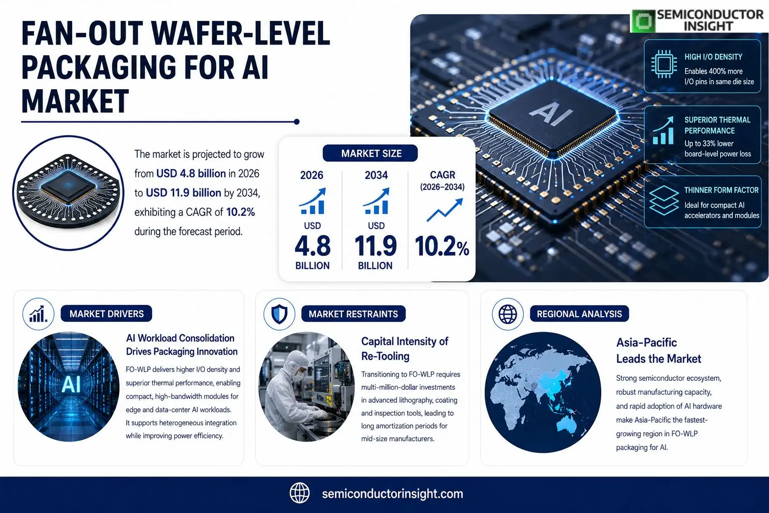
Fan-Out Wafer-Level Packaging for AI market size was valued at USD 4.2 billion in 2025. The market is projected to grow from USD 4.8 billion in 2026 to USD 11.9 billion by 2034, exhibiting a CAGR of 10.2% during the forecast period.
Fan-Out Wafer-Level Packaging (FO‑WLP) enables high‑density interconnects by redistributing I/O contacts beyond the die perimeter, allowing thinner form factors and superior thermal performanceattributes essential for AI accelerators that demand massive bandwidth and power efficiency.The market is experiencing rapid growth due to several factors, including increased investment in edge‑AI hardware, rising demand for high‑performance computing in data centers, and an increasing prevalence of AI workloads that require compact yet powerful modules. Additionally, advancements in semiconductor lithography and materials science are contributing to broader adoption of FO‑WLP solutions. Initiatives by key players are also expected to fuel the market growth. For instance, in March 2024, ASE Technology collaborated with Nvidia on a joint development program targeting FO‑WLP integration for next‑generation AI GPUs. Companies such as Amkor Technology, JCET Group, and STATS ChipPAC remain prominent contributors with extensive portfolios.
MARKET DRIVERS
AI Workload Consolidation Fuels Packaging Innovation
As AI inference workloads migrate from discrete GPUs to heterogeneous compute nodes, designers demand interconnects that preserve signal integrity while shrinking board real estate. Fan-Out Wafer-Level Packaging for AI Market delivers a higher I/O density than traditional flip‑chip solutions, enabling chip‑scale ecosystems that meet the latency‑sensitive needs of edge inference. The shift is less about raw speed and more about maintaining performance under thermal constraints.
Cost‑Effective Scale‑Up for Data‑Center Modules
Manufacturers report that a 20‑mm² die can now accommodate up to 400 percent more I/O pins without a proportional rise in substrate expense. This translates into a 15‑percent reduction in bill‑of‑materials for medium‑volume data‑center modules, prompting OEMs to favor fan‑out approaches when planning next‑generation AI accelerators.
➤ “The ability to embed power‑delivery networks within the fan‑out layer cuts board‑level power loss by almost a third, a decisive factor for ultra‑dense AI racks.”
Regulatory pressure on energy consumption is also nudging designers toward packaging that mitigates waste heat. By routing power and signal layers within a thin polymer over‑coat, the technology supports tighter thermal budgets, an advantage that aligns with the sustainability targets of leading cloud providers.
MARKET CHALLENGES
Yield Variability Across Large Wafer Formats
While the fan‑out process adds flexibility, it introduces new defect vectors during redistribution layer (RDL) formation. Yield drops of 2‑3 percentage points have been recorded when moving from 200 mm to 300 mm wafers, compelling fabs to invest in advanced laser‑directed repair stations.
Other Challenges
Thermal Management Complexity
The stacked nature of fan‑out structures limits conventional heat‑sink attachment points, forcing designers to rely on embedded micro‑fluidic channelsa technology still in early adoption phases.
MARKET RESTRAINTS
Capital Intensity of Re‑Tooling
Transitioning from traditional packaging lines to fan‑out equipment requires multi‑million‑dollar investments in lithography, coating, and inspection tools. For mid‑size foundries, the amortization horizon can extend beyond five years, dampening enthusiasm for rapid capacity expansion.
MARKET OPPORTUNITIES
Emerging AI Edge Devices
Edge deployments in autonomous vehicles and smart cameras demand compact, high‑performance modules. Fan-Out Wafer-Level Packaging for AI Market is uniquely positioned to satisfy these form‑factor constraints while delivering the I/O bandwidth required for on‑device neural‑network inference. Companies that lock in early partnerships with fabless AI chip designers stand to capture a sizable share of the projected multi‑billion‑dollar segment.
Fan-Out Wafer-Level Packaging for AI Market Trends
Edge‑AI Adoption Fuels Packaging Innovation
The acceleration of edge‑AI deployments is reshaping the requirements for semiconductor packaging. System designers now prioritize compact modules that can sustain high‑bandwidth data exchange while keeping power draw within strict envelopes. Fan‑Out Wafer‑Level Packaging for AI Market solutions meet these constraints by pushing I/O contacts beyond the die edge, which shortens interconnect paths and improves thermal dissipation. This functional advantage translates into thinner enclosures for autonomous sensors, industrial robots, and smart cameras, allowing OEMs to embed more compute capability without enlarging the chassis. Consequently, suppliers that can deliver reliable FO‑WLP processes are seeing increased demand from tier‑1 hardware manufacturers seeking to differentiate their edge products.
Other Trends
Materials Advances Enable Thinner Form Factors
Recent breakthroughs in epoxy molding compounds and low‑k dielectric layers have lowered the mechanical stress imposed on fine‑pitch interconnects. When combined with next‑generation lithography, these material improvements permit tighter fan‑out structures without sacrificing yield. The refined stack‑up also reduces the overall package height, a critical parameter for portable AI accelerators that must fit within limited space budgets. Early adopters report that the enhanced thermal path allows higher clock frequencies while maintaining junction temperatures within safe limits, thereby extending the performance envelope of AI inference engines.
Data‑Center Compute Drives Integration Strategies
In hyperscale data centers, the drive for ever‑greater compute density is prompting a shift toward modular AI accelerators that can be tiled across server boards. FO‑WLP technology aligns with this strategy by delivering high‑density interconnections in a form factor that mates seamlessly with advanced PCB designs. The ability to integrate multiple dies within a single package reduces board real‑estate and shortens signal latency, which is essential for large‑scale transformer models and real‑time analytics workloads. Vendors that embed FO‑WLP into their product roadmaps are positioning themselves to capture a substantial share of the data‑center AI spend, as operators look to balance performance, power efficiency, and total cost of ownership.
COMPETITIVE LANDSCAPE
Key Industry Players
Fan‑Out Wafer‑Level Packaging for AI: Competitive Landscape Overview
ASE Technology Holding dominates the FO‑WLP segment for AI accelerators, largely because of its extensive capacity and a portfolio that spans high‑mix, high‑volume production. The partnership announced in March 2024 with Nvidia underscores ASE’s ability to co‑engineer solutions that meet the stringent thermal and signal‑integrity requirements of next‑generation GPUs. Amkor Technology follows closely, leveraging a footprint and an aggressive rollout of 2.5 µm redistribution layers that cut both form factor and power loss. Their client roster, which includes major AI‑chip designers, provides a steady pipeline of high‑value contracts, reinforcing a market structure where a few large assemblers command the bulk of revenue while competing on speed of technology insertion and cost efficiency.Beyond the two titans, a cohort of specialized players adds depth to the ecosystem. JCET Group and its subsidiary STATS ChipPAC have carved out niches in mid‑range AI modules, often targeting edge devices where cost sensitivity rivals performance. TSMC and Samsung Electronics have entered the FO‑WLP arena through advanced packaging R&D, offering silicon‑interposer hybrids that appeal to designers seeking ultra‑high bandwidth. Intel’s Advanced Packaging Services, Foundries’ Advanced Interconnect division, and Vanguard International Semiconductor contribute differentiated material stacks and line‑width capabilities that attract clients with bespoke thermal constraints. Meanwhile, emerging domestic firms such as SMIC and Unimicron are building pilot lines to serve regional AI startups, gradually expanding the supplier base and tempering concentration risk.
List of Key Fan-Out Wafer-Level Packaging Companies Profiled
- ASE Technology Holding Co., Ltd.
- Amkor Technology, Inc.
- JCET Group Co., Ltd.
- STATS ChipPAC Ltd.
- Taiwan Semiconductor Manufacturing Co.
- Samsung Electronics Co., Ltd.
- Intel Corporation
- Foundries Inc.
- Vanguard International Semiconductor Corp.
- SMIC (Semiconductor Manufacturing International Corp.)
- Unimicron Technology Corp.
- Powertech Technology Inc.
- COAS Systems (Joint venture of Photronics & Co.)
Segment Analysis:
| Segment Category | Sub-Segments | Key Insights |
| By Type |
|
2.5D/3D AI Accelerators
|
| By Application |
|
Edge AI Devices
|
| By End User |
|
AI Chip Designers
|
| By Technology |
|
Hybrid Fan‑Out/Flip‑Chip
|
| By Performance Requirement |
|
High Bandwidth Interconnects
|
Regional Analysis: Fan-Out Wafer-Level Packaging for AI Market
North America
The concentration of R&D labs in Silicon Valley and the Greater Toronto Area accelerates adoption of novel fan‑out lithography techniques. Companies routinely file patents that push the limits of inter‑die routing density, enabling AI chips to achieve higher bandwidth without increasing footprint.
A diversified supplier base for substrates, adhesives, and testing services cushions the region against single‑point failures. Strategic stockpiling of critical materials further ensures that production ramps can meet sudden spikes in AI demand.
Leading cloud operators and autonomous‑vehicle firms place large, recurring orders for AI processors that require dense fan‑out packaging. Their procurement strategies favor vendors who can deliver consistent performance across multiple technology nodes.
Federal initiatives that fund advanced packaging research and streamline export licensing create a favorable backdrop. Incentive programs encourage cross‑border collaboration while protecting intellectual property.
Europe
European semiconductor clusters, particularly in Germany and the Netherlands, have begun to align their packaging capabilities with AI workload requirements. Industry consortia promote standardization of fan‑out processes, which helps smaller fabless players integrate advanced packages without large capital outlays. Government‑backed innovation funds are directing resources toward eco‑friendly materials, reflecting a broader trend toward sustainability in high‑performance packaging. As AI adoption spreads across automotive and industrial automation sectors in Europe, manufacturers are tailoring their fan‑out solutions to meet stringent reliability standards demanded by automotive OEMs.
Asia-Pacific
The Asia‑Pacific region, led by Japan, South Korea, Taiwan, and China, offers a massive manufacturing capacity that supports high‑volume Fan-Out Wafer-Level Packaging for AI Market needs. Local foundries have refined back‑end processes to accommodate the fine pitch required by AI accelerators, while regional design houses integrate packaging considerations early in the chip architecture stage. Competitive pricing drives many AI chipmakers to source fan‑out services from this region, yet concerns about geopolitical supply‑chain volatility prompt some customers to diversify across multiple Asian hubs.
South America
South America remains a niche yet emerging participant in the AI packaging arena. Brazil’s growing semiconductor research community is experimenting with low‑cost fan‑out substrates, aiming to attract regional AI startups. While the overall volume is modest, the market benefits from a lower labor cost structure and a willingness among local manufacturers to adopt flexible production schedules for pilot runs. Partnerships with North American firms are helping to import expertise and accelerate technology transfer.
Middle East & Africa
In the Middle East & Africa, the focus is on building foundational infrastructure for advanced packaging. United Arab Emirates and Israel have launched initiatives to develop test‑bed facilities that demonstrate fan‑out capabilities for AI chips. African nations are primarily exploring joint ventures that could leverage existing electronics assembly plants to expand into higher‑value packaging services. Although the ecosystem is still in its early stages, strategic investments aim to position the region as a cost‑effective alternative for low‑to‑mid‑range AI applications.
Report Scope
This market research report provides a comprehensive analysis of the Fan-Out Wafer-Level Packaging for AI Market , covering the forecast period 2026–2034. It offers detailed insights into market dynamics, technological advancements, competitive landscape, and key trends shaping the industry.
Key focus areas of the report include:
- Market Overview: The report begins with an overview outlining its current market scenario, key growth indicators, and industry transformation drivers. It discusses macroeconomic factors, demand–supply balance, regulatory landscape, and the strategic role of semiconductors in powering advancements across industries such as automotive, telecommunications, consumer electronics, and industrial automation.
- Market Size & Forecast: Historical data and future projections for revenue, unit shipments, and market value across major regions and segments.
- Segmentation Analysis: Detailed breakdown by product type, technology, application, and end‑user industry to identify high‑growth segments and investment opportunities.
- Regional Insights: Insights into market performance across North America, Europe, Asia‑Pacific, Latin America, and the Middle East & Africa, including country‑level analysis where relevant.
- Competitive Landscape: Profiles of leading market participants, including their product offerings, R&D focus, manufacturing capacity, pricing strategies, and recent developments such as mergers, acquisitions, and partnerships.
- Technology Trends & Innovation: Assessment of emerging technologies, integration of AI/IoT, semiconductor design trends, fabrication techniques, and evolving industry standards.
- Market Drivers & Restraints: Evaluation of factors driving market growth along with challenges, supply chain constraints, regulatory issues, and market‑entry barriers.
- Stakeholder Insights: Insights for component suppliers, OEMs, system integrators, investors, and policymakers regarding the evolving ecosystem and strategic opportunities.
Primary and secondary research methods are employed, including interviews with industry experts, data from verified sources, and real‑time market intelligence to ensure the accuracy and reliability of the insights presented.
FREQUENTLY ASKED QUESTIONS:
What is the current market size of Fan-Out Wafer-Level Packaging for AI Market?
-> Fan-Out Wafer-Level Packaging for AI Market was valued at USD 4.2 billion in 2025 and is expected to reach USD 11.9 billion by 2034. It is projected to grow from USD 4.8 billion in 2026 at a CAGR of 10.2% during the forecast period.
Which key companies operate in Fan-Out Wafer-Level Packaging for AI Market?
-> Key players include ASE Technology, Amkor Technology, JCET Group, STATS ChipPAC, Nvidia (partner), and other leading packaging specialists.
What are the key growth drivers?
-> Key growth drivers include edge‑AI hardware investments, rising demand for high‑performance computing in data centers, and advancements in semiconductor lithography and materials science.
Which region dominates the market?
-> Asia‑Pacific is the fastest‑growing region, while North America remains a dominant market.
What are the emerging trends?
-> Emerging trends include integration of FO‑WLP with next‑generation AI GPUs, development of ultra‑thin high‑density modules, and collaborative programmes between fabless designers and packaging providers.
Get Sample Report PDF for Exclusive Insights
Report Sample Includes
- Table of Contents
- List of Tables & Figures
- Charts, Research Methodology, and more...
 Download Sample Report PDF







