Key Statistics
Key Takeaways
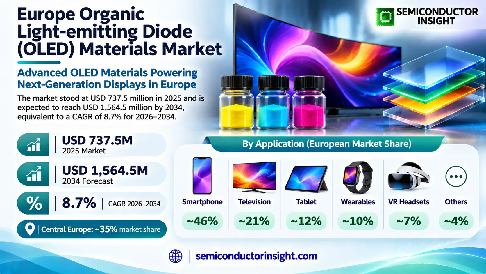
- OLED materials revenue in Europe is projected to rise from USD 737.5 million in 2025 to USD 1,564.5 million by 2034 at a 8.7% annual rate, supported by advanced emissive and charge-transport chemistry across display form factors.
- AMOLED technology accounts for an estimated ~92% of material value because its independently driven pixels dominate premium smartphone, tablet and large display manufacturing; PMOLED remains a relatively specialized low-complexity product with ~8% share.
- Smartphone materials retain the leading estimated ~46% application share, while televisions account for ~21%, tablets ~12%, wearables ~10%, near-eye VR devices ~7% and other uses ~4% across the European market.
- Central Europe leads at an estimated ~35% share through German materials companies, chemical expertise and display research, while Western Europe holds about ~30% and Northern Europe about ~12% of regional value.
- Materials research advances include Novaled transport and doping compounds, Merck livilux products, UDC phosphorescent emitters and research into high-efficiency blue stacks, while former independent Cynora technologies are owned by Samsung Display.
Europe Organic Light-emitting Diode (OLED) Materials Market Overview
Europe organic light-emitting diode (OLED) materials market stood at USD 737.5 million in 2025 and is expected to reach USD 1,564.5 million by 2034, equivalent to a CAGR of 8.7% for 2026–2034. Central Europe represents an estimated ~35% share, with German specialty-chemicals capability and materials engineering among its commercial strengths.
Organic light-emitting devices create light when charge carriers recombine in thin molecular layers between two electrical contacts. Commercial OLED stacks combine several functional organic compounds, including hole transport, electron transport, injection dopants, exciton blocking layers, emitting molecules and host materials. A display pixel is an engineered multilayer system, so a manufacturer cannot usually substitute one chemical for another without evaluating lifetime, power use and interactions throughout the stack.
The revenue boundary concerns the specialty chemicals used to manufacture OLED display and lighting structures marketed in Europe, across passive-matrix and active-matrix architectures. It excludes the retail value of smartphones, complete TV panels, finished vehicle displays, semiconductor backplane chips and standalone evaporation machinery. Material suppliers can be established in Germany or Japan, while panel fabrication and final device consumption occur elsewhere; these are different links in the value chain.
Purity and repeatability are central competitive variables. Merck describes purified materials suitable for vacuum evaporation on rigid and flexible substrates, while Novaled develops transport-layer doping that can lower operating voltage and improve stability. Phosphorescent emitters capture additional excited-state energy compared with conventional fluorescent molecules, creating an efficiency opportunity, though blue emitter lifetime and manufacturability remain active development challenges.
Commercial momentum comes from premium displays and expanding use cases rather than uniform substitution of every display technology. Thin flexible OLEDs can support curved interfaces and foldable phones, while near-eye microdisplays impose extremely tight pixel and brightness demands. Materials must withstand oxygen and moisture during storage and operation, and suppliers need to demonstrate compatibility with customers’ deposition recipes. Qualification cycles can therefore be lengthy even for promising laboratory molecules.
Segment Analysis: By Type
AMOLED-related materials account for an estimated ~92% of European value because active-matrix addressing is used for high-resolution phones, tablets, televisions and many wearables. Passive-matrix OLED contributes roughly ~8% and is concentrated in smaller, simpler or specialist displays where backplane cost and basic functionality matter more than continuous high-brightness multimedia performance. These are device architecture groups rather than isolated individual chemical categories.
| Type | Function | Market position |
|---|---|---|
| PMOLED | Passive-matrix OLED structures activate pixels through crossing electrode lines rather than dedicated thin-film-transistor control of each individual pixel. This can suit simple status indicators, small segment displays and some industrial modules. Organic emitters and transport materials remain necessary, but the lower screen complexity generally limits material value for each unit compared with larger active-matrix applications. | Specialized architecture, estimated ~8% share, ~3.3% CAGR. PMOLED demand reflects practical low-content product niches and replacement devices rather than the largest premium consumer markets. Buyers emphasize long storage life, reliable uniformity, visible output and supplier continuity. Material spending can remain stable even when the number of active-matrix pixels in consumer equipment rises far more quickly. |
| AMOLED | Active-matrix panels address subpixels using an electronic backplane, supporting high resolution and controlled brightness in phones, TVs and near-eye devices. Their stack can include proprietary emitters, hosts, injection chemistry and several transport layers. A small improvement in carrier balance can affect power consumption and aging across a huge number of pixels, making material qualification commercially significant. | Dominant architecture, estimated ~92% share, ~9.1% CAGR. Demand spans flexible smartphones, premium tablets and large-area display fabrication. Suppliers compete on molecule purity, lifetime under production driving conditions and compatibility with evaporation or emerging deposition processes. The material content of a device depends on the layer configuration and panel area; it does not simply follow the count of displays shipped. |
Segment Analysis: By Application
Smartphone material applications represent an estimated ~46% of European value, followed by television at ~21%, tablets at ~12%, wearables at ~10%, VR headsets at ~7% and other products at ~4%. The emphasis differs by form factor: pocket devices prioritize efficiency and thinness, television panels use much larger active areas, while near-eye systems need extraordinarily small pixels and carefully controlled optics.
| Application | Demand characteristics |
|---|---|
| Smart Phone | Largest application, estimated ~46% share, ~7.9% CAGR. Premium smartphones require flexible or rigid high-resolution OLED panels with stable colors and acceptable battery consumption. Organic compounds must survive demanding duty cycles and repeated thermal changes, especially in foldable products. Material suppliers win design qualification by improving reliability at production scale rather than by demonstrating a single excellent laboratory pixel. |
| VR Helmet | High-growth niche, estimated ~7% share, ~12.1% CAGR. Virtual reality and mixed-reality headsets place a premium on miniature display structures, visual response and optical efficiency. Fraunhofer IPMS demonstrated a 720 x 540-pixel RGBW microdisplay on 28nm CMOS in 2026, illustrating the precision required. The device evidence is adjacent technology context, not an independent measurement of regional organic material revenue. |
| Wearable Device | Estimated ~10% share, ~9.2% CAGR. Smartwatches and lightweight wearables benefit from OLED contrast and power management because they operate from compact batteries. Strong performance depends on charge balance and lifetime at the brightness needed in everyday use. Material purchases for these devices may be small per unit but demanding in qualification due to thin form factors and temperature exposure. |
| Tablets | Estimated ~12% share, ~10.4% CAGR. Premium tablets and convertible computers extend active-matrix OLED to larger surfaces than phones. This can increase the material consumption per panel while emphasizing uniform color and low defects. Suppliers must demonstrate repeatable deposition and acceptable lifetime across the larger active area. Product qualification may be coordinated with new generation display lines. |
| TV | Estimated ~21% share, ~8.0% CAGR. Large television panels consume organic material over substantially greater area than handheld displays. Uniformity and production yield consequently have major economic significance. Transport dopants, stable emitters and carefully selected host materials can improve the operating balance, but alternatives such as LCD and evolving mini-LED displays still compete on cost and brightness. |
| Other | Estimated ~4% share, ~8.4% CAGR. Automotive displays, specialty instrumentation, emerging OLED lighting and research devices create a varied smaller segment. Automotive products demand durability across temperature changes, while lighting structures can benefit from thin, area-emitting surfaces. Material buyers need to establish which optical characteristics and safety requirements belong to the actual application rather than assuming display-grade compounds automatically suit every use. |
OLED material consumption follows the chemistry and architecture of the final device, not merely its screen size. A premium phone may incorporate many precision-deposited layers, and a large TV offers a different area-driven demand profile. An individual organic compound can have several customer uses only after it passes device-specific reliability and process qualification. Emerging applications often introduce new material requirements before they deliver commercial scale.
Regional Analysis
Central Europe represents an estimated ~35% of Europe OLED materials value, closely followed by Western Europe at ~30%. Northern Europe accounts for about ~12%, Southern Europe for ~15% and Eastern Europe for ~8%. These five European clusters reflect specialty chemical suppliers, research facilities, product design, imports and end-device consumption; they are not a claim that all panels are fabricated in Europe.
Where is the strongest European OLED materials activity and what differentiates national demand?
Germany stands out for chemical materials development, with Merck and Novaled establishing substantial local technical capability. France, the United Kingdom and Benelux contribute engineering, imported electronics and downstream equipment markets. Nordic research and industrial customers demand efficient display solutions; Southern and Eastern Europe have further application and distribution activity. Material revenue requires care in attribution because molecule supply, display panel fabrication and consumer device sales frequently cross national boundaries.
| Region | Position | Growth outlook | Demand profile | What decides supplier selection |
|---|---|---|---|---|
| Central Europe | Largest (~35%) | ~8.3% CAGR | Specialty chemicals and device-layer research | Purity and fabrication qualification |
| Western Europe | Estimated ~30% | ~8.8% CAGR | Electronics design and premium device demand | Material performance and import logistics |
| Northern Europe | Estimated ~12% | ~9.7% CAGR | Research, advanced optics and connected products | Lifetime and efficiency verification |
| Southern Europe | Estimated ~15% | ~8.4% CAGR | Consumer electronics and industrial design | Component access and cost control |
| Eastern Europe | Estimated ~8% | ~9.1% CAGR | Electronics assembly and specialized display adoption | Qualified distributors and consistent quality |
Key Europe Organic Light-emitting Diode (OLED) Materials Manufacturers and Competitive Landscape
European OLED materials competition blends regional specialty-chemicals producers, overseas emitter licensors and international display manufacturers. Merck operates its livilux OLED portfolio, Novaled supplies charge transport and doping compounds, and Universal Display Corporation licenses phosphorescent technology and markets associated emitters and hosts. Idemitsu develops blue material stacks. Former independent Cynora technology was acquired by Samsung Display in 2022, and equipment companies should not be represented as equivalent chemical suppliers.
Merck KGaA in Germany competes with purified molecular materials that panel manufacturers can evaporate onto rigid and flexible substrates. Its organic portfolio includes hole and electron transport compounds, host or matrix chemistry and blocking materials. Commercial strength depends on precision purification, documentation and formulation consistency across lots, since the panel maker must fit a proposed molecule within a complete process. European proximity to research institutions helps technical exchanges even when the high-volume fabrication plant is in Asia.
Novaled, headquartered in Germany and majority-owned by Samsung SDI, is a specialist in doping and transport-layer organic chemistry. It describes improved charge carrier mobility and lower operating voltage as important advantages. These are non-emissive layer contributions rather than a direct substitute for every phosphorescent emitter. Its August 2025 patent update concerned transport chemistry, a reminder that suppliers compete through intellectual property and manufacturing implementation as well as measured optical performance.
Universal Display Corporation focuses on proprietary phosphorescent OLED materials and associated architecture patents. Its commercial red, green and yellow materials and host systems are distinct from the continuing effort to commercialize improved blue emitters. In August 2026 the company unveiled OLEDX, a different device architecture intended to improve light extraction, while in November it announced work with OLEDWorks on cyan automotive communication lighting. Those activities indicate technology direction rather than audited European chemistry sales.
Idemitsu Kosan and other Japanese and Korean companies contribute key upstream materials and development capacity. Idemitsu announced in 2025 a blue OLED performance result involving stacked fluorescent-emission layers; this illustrates the competitive pressure to improve efficient, durable blue pixels. AIXTRON supplies fabrication equipment and is best treated as an adjacent process enabler. Historical Cynora work is relevant to blue materials, but an acquisition should not be presented as an active independent chemical supplier.
Tier structure
| Tier | Companies | Basis of competition |
|---|---|---|
| Specialty OLED chemistry | Merck KGaA, Novaled GmbH | German-based suppliers market distinct combinations of OLED organics, including purified matrix materials, doping and charge-transport layers. Customer relationships depend on qualifications that span chemistry, deposition conditions and many operating cycles. Both may support international factories even when work is carried out in European laboratories. |
| Emitter technology and hosts | Universal Display Corporation, Idemitsu Kosan, Sumitomo Chemical | International materials and IP companies supply phosphorescent or fluorescent emitters and other stack components. Commercial differentiation comes from the balance of efficiency, color, operating voltage and lifetime, plus the cost and usability of a material in a manufacturing recipe. Technical demonstrations are not identical to recurring sales. |
| Adjacent technologies and research | Fraunhofer research institutes, AIXTRON process equipment, display qualification partners | Research and deposition-equipment firms influence the methods used to develop and handle OLED materials, but a piece of equipment is not the same revenue object as an organic compound. They can shape future demand through microdisplay designs, process options and quality control, yet their commercial exposure needs separate treatment. |
Key companies profiled
- Merck KGaA
- Novaled GmbH (Samsung SDI majority ownership)
- Universal Display Corporation
- Idemitsu Kosan
- Sumitomo Chemical
- BASF SE (specialty chemistry; verify specific OLED products)
- Cynora technology (acquired by Samsung Display in 2022)
Europe Organic Light-emitting Diode (OLED) Materials Production Capacity Analysis
OLED organic materials production begins with precise chemical synthesis and purification, then controlled packaging, analytical testing and delivery to device fabricators. The materials are subsequently deposited into nanometre-scale functional layers by methods such as vacuum thermal evaporation or selected solution processes. The purity and repeatability requirements create a different capacity model from finished OLED panel production; a chemistry site can supply multiple panel factories across continents.
Organic emitters, hosts and carrier-transport molecules are synthesized in chemical batches and isolated through purification steps intended to reduce trace impurities. Merck describes high-purity compounds suitable for evaporation, while Novaled designs dopants and transport materials to fit commercial layer stacks. Product development uses spectroscopy, thermal analysis and device qualification because a molecule that looks promising in isolation may fail when used with a particular electrode or neighboring organic material.
Vacuum deposition remains common for high-performance OLED fabrication. The chemical must vaporize and condense predictably without degrading or depositing uncontrolled contaminants. Other approaches include ink formulations and patterned printing, which may improve material efficiency but introduce solvent, drying and resolution challenges. Fraunhofer IAP notes that printing methods can reduce wasted material relative to shadow-mask evaporation, although fine pixel pitches make commercial implementation demanding.
Capacity depends on the ability to make consistent high-purity lots and on panel-factory qualification, not merely a nominal reactor volume. Chemical makers must document the identity of batches, storage conditions, safety procedures and properties after transport. A global material company may sell to customers in Asia while performing development and purification in Europe. Device companies will often retain a mature material stack unless a change provides a compelling efficiency or lifetime advantage.
Europe Organic Light-emitting Diode (OLED) Materials Market Dynamics: Drivers, Restraints and Opportunities
OLED materials demand grows with premium active-matrix screen adoption, advances in efficient emissive chemistry and the expansion of display formats beyond phones. Material costs, difficult blue lifetime targets, manufacturing yield and competition from other display technologies moderate the trajectory. Customer qualification is a durable source of supplier advantage because changing a molecule can alter electrical and optical characteristics across several layers of the finished device.
MARKET DRIVERS
Drivers Impact Analysis*
| Market Drivers | Impact Rank | CAGR Contribution (%) | 2026–2028 | 2029–2031 | 2032–2034 |
|---|---|---|---|---|---|
| AMOLED penetration in personal electronics | High | +4.60% | High | High | High |
| Efficiency and longer-life materials | Medium-High | +3.20% | High | High | High |
| TV and IT display expansion | Medium | +2.40% | Medium | High | High |
| Near-eye microdisplay innovation | Low-Medium | +1.40% | Medium | High | High |
| Others (automotive and specialty lighting) | Low | +0.90% | Medium | Medium | High |
Premium AMOLED use sustains demand for specialized layers
High-end phones, tablets and watches increasingly rely on active-matrix OLED screens that combine multiple functional organic compounds. Even a thin deposit can become a material requirement across many pixels, especially where the manufacturer seeks uniform performance at commercial scale. The relevant purchasing decision is made by the panel producer after testing the device stack, so suppliers benefit when their chemistry is qualified for a successful platform generation.
Phosphorescent materials offer an efficiency advantage
Organic emitter chemistry determines how effectively electron and hole recombination generates visible light. Universal Display markets phosphorescent emitters and hosts that enable more efficient operation than traditional fluorescence in particular implementations. Commercial customers evaluate not only a headline efficiency gain but also operating voltage, long-term color stability and fabrication yield. The work on blue emission remains significant because white balance and panel lifetime depend on every primary color.
Large and medium screens increase material opportunities
The extension of OLED into televisions, tablets and laptop panels raises attention to uniform deposition over larger areas. Bigger screens can consume more total organic material per device and require carefully selected host and transport layers. A panel maker may reject an otherwise efficient molecule if it raises defect rates or creates unacceptable aging differences across the screen. Process-compatible chemistry therefore supports commercialization as much as laboratory optical performance.
Near-eye displays stimulate advanced stack development
Microdisplays used in headsets need very fine pixels and sufficient brightness after optical losses. Fraunhofer IPMS presented a 28nm CMOS-backed OLED microdisplay during September 2026, demonstrating active European research into this device class. The project itself is not a material sales disclosure, but it highlights technical problems—uniformity, heat, luminous efficiency and color—that influence future molecular design and panel-manufacturing choices.
MARKET RESTRAINTS
Restraints Impact Analysis*
| Market Restraints | Impact Rank | CAGR Contribution (%) | 2026–2028 | 2029–2031 | 2032–2034 |
|---|---|---|---|---|---|
| High-purity synthesis and qualification cost | High | -1.80% | High | High | Medium |
| Blue lifetime and manufacturing yield | Medium-High | -1.30% | High | High | High |
| Alternative display technologies | Medium | -0.50% | Medium | High | High |
| Others (supply and process risks) | Low | -0.20% | Medium | Medium | Medium |
Material qualification consumes time and resources
Panel manufacturers qualify a chemical through many iterations of recipe tuning, deposition trials and long-duration operation tests. A different compound can affect contact resistance, optical cavity behavior and adjacent layers, making simple drop-in substitutions uncommon. Specialty synthesis, purification and the protection of proprietary formulas add expense. Suppliers without consistent large-lot quality struggle to convert laboratory successes into dependable recurring contracts.
Blue efficiency and durability remain difficult
High-energy blue emission can accelerate some degradation mechanisms, while users still expect acceptable brightness and color stability over years. Material developers have explored phosphorescent blue, stacked fluorescent structures and other architectures, but each option must perform under actual operating current and process conditions. Claims of improved laboratory performance should therefore be assessed against device life and manufacturing yield before being treated as fully commercial replacements.
OLED competes with alternative display structures
LCD technology remains competitive for large and price-sensitive screens, including systems using advanced backlights. MicroLED and other emerging architectures may eventually serve different brightness or durability requirements, though manufacturing scale and cost remain important issues for them too. OLED material suppliers have to continue improving lifetime, color performance and efficiency so their technology retains advantages where customers value form factor and pixel-level control.
MARKET OPPORTUNITIES
Better blue emitters and layer combinations
Material developers can capture additional value if new blue molecules or stacked structures improve efficiency without sacrificing useful life. Idemitsu has reported progress with dual emitting-layer blue devices, and Universal Display continues its phosphorescent blue programme. Manufacturers must still prove repeatability and compatibility with other stack materials. The commercial prize is potentially broad because blue emission is a common performance constraint across many OLED formats.
Display devices with challenging shapes
Flexible, curved and foldable OLEDs expand the need for molecules that remain stable when paired with very thin barrier structures and demanding product packaging. A company that supplies a reliable transport layer or emitter can earn a place in a new architecture even if its chemistry is only a small fraction of the finished device value. The challenge is coordinating materials innovation with substrate and encapsulation technologies.
Microdisplay brightness and color fidelity
Near-eye panels create demanding optical requirements that may favor new emissive materials, tandem structures and tailored hosts. Smaller pixels also narrow manufacturing tolerances, so materials must work with suitable patterning and device designs. European research programmes offer test opportunities, but a commercial supplier needs to translate demonstrations into manufacturable specifications. Collaboration across chip backplanes, organic chemistry and optics can create differentiated products.
Printable organic electronics and material efficiency
Printing approaches can deposit some organic materials only where pixels need them, potentially reducing waste from vacuum shadow masks. Fraunhofer research describes limitations in resolution that must be overcome for the highest-density screens. Specialty ink formulations, solvent stability and interface control represent possible commercial openings. Progress should be assessed against lifetime and yield rather than assuming a printed film automatically replaces well-established evaporation processes.
Europe Organic Light-emitting Diode (OLED) Materials Supply Chain Analysis
OLED organic materials move from research chemistry and synthesis into purification, measured quality control, protective packaging and shipment to thin-film display manufacturers. Device producers combine selected emitters, hosts, transport materials, electrodes and encapsulation into a qualified panel stack. The important commercial interfaces are molecule-to-process compatibility, batch consistency and the speed with which a supplier can support changes at a fabrication line.
Synthesis and specialist purification. Organic molecules are built through controlled chemistry where unwanted impurities can affect electrical properties and operating life. Manufacturing scale becomes useful only when the batch can be repeated at the required purity and composition. Analytical records enable customers to compare a pilot sample with delivered commercial material. Logistics, moisture protection and handling practices are part of quality because a satisfactory compound can degrade before it reaches the deposition tool.
OLED material stack integration. Transport layers, emitting layers and blocking layers interact electrically and optically, requiring panel fabricators to tune the full stack. Novaled supplies dopants and transport chemistry while other companies deliver emitters or hosts. Even a small change in an interface can shift the balance of carriers and affect color or voltage. Device qualification consequently requires sustained supplier collaboration rather than merely buying a molecule that has attractive isolated properties.
Fabrication and process-equipment links. OLED materials are applied through controlled thin-film processes such as vacuum thermal evaporation or developing printing routes. Process-equipment companies can influence demand by supporting lower waste or improved deposition accuracy, but they do not automatically sell the same organic chemicals. A material supplier must understand evaporation stability, cleaning procedures and how a recipe affects defect rates. The production route shapes price and qualification requirements at each customer.
Device makers and market feedback. Panel manufacturers combine the compounds into screen technology, then deliver displays to consumer electronics and industrial brands. A change in display form factor may produce a new molecular challenge long before the final product launches. Material producers work with fabrication customers on endurance data and consistent supplies. Cross-border chains are common, so European demand should be interpreted with attention to where chemistry is produced, purchased and incorporated.
Recent Developments in the Europe Organic Light-emitting Diode (OLED) Materials Market
- 9 November 2026 Automotive OLED research
Universal Display Corporation and OLEDWorks announced an evaluation programme for cyan OLED lighting intended for automated-driving communication. The work joins phosphorescent light-emission chemistry with panel development, offering a possible specialized materials application. It should not be presented as a confirmed volume contract or as part of current smartphone material shipments. Its importance is the widening set of device architectures that can require controlled organic emission. Source - 28 October 2026 Materials technology
Universal Display reported its third-quarter 2026 results and discussed ongoing phosphorescent blue development, materials discovery and new device architectures. These activities reinforce the commercial attention on efficiency and performance across displays. The release concerns a global technology provider and does not disclose a standalone European materials-market share; regional sales must be distinguished from company-wide financial measures. Source - 21 September 2026 Microdisplay demonstration
Fraunhofer IPMS announced a full-color RGBW OLED microdisplay using 28nm CMOS and a 720 by 540 pixel arrangement. The announcement shows how smaller near-eye panels can demand high optical efficiency and precise layer engineering. It is evidence of ongoing European research rather than proof that a particular emitter chemistry is now in mass production or that consumer headset volumes are already secured. Source - 19 August 2026 OLED architecture
Universal Display unveiled its OLEDX architecture as an approach to improve OLED light utilization and viewing control. Advances of this kind may shift future demands on emitters, transport layers and optical design, but customers will still need to qualify specific implementations. The disclosure should be read as a global engineering development, not as direct confirmation of revenue attributable to organic materials sold in Europe. Source - 15 August 2025 OLED materials patents
Novaled announced the outcome of Korean patent disputes relating to electron-transport materials and organic electronic emissions. The announcement highlighted the importance of intellectual property to differentiated materials technology. Patent decisions can affect competitive risk and supply choices, but they do not replace technical qualification of a particular panel chemistry. The company continues to offer transport and doping materials within its current ownership structure. Source
REPORT SCOPE & SEGMENTATION
| Attribute | Details |
|---|---|
| Study Period | 2020–2034 |
| Base Year | 2025 |
| Estimated Year | 2026 |
| Forecast Period | 2026–2034 |
| Historical Period | 2020–2024 |
| Market Size 2025 | USD 737.5 million |
| Market Size 2026 | USD 801.8 million |
| Market Size 2034 | USD 1,564.5 million |
| Growth Rate | CAGR of 8.7% during 2026–2034 |
| Unit | Value in USD million for organic light-emitting material compounds |
| Segmentation | By OLED Products Type, By Application and By European Subregion |
| By Products Type | PMOLED; AMOLED |
| By Application | Smart Phone; VR Helmet; Wearable Device; Tablets; TV; Other |
| By Region | Europe-only market across five European subregions; named country markets include Germany, United Kingdom, France, Italy, Spain, Netherlands, Belgium Central EuropeGermany, Austria, Switzerland Western EuropeFrance, United Kingdom, Netherlands Northern EuropeSweden, Denmark, Finland Southern EuropeItaly, Spain, Portugal Eastern EuropePoland, Czech Republic, Romania |
| Key Companies Profiled | Merck KGaA; Novaled / Samsung SDI; Universal Display Corporation; Idemitsu Kosan; Sumitomo Chemical; BASF; acquired Cynora technology within Samsung Display |
| Customization Scope | Available research topics include emitter chemistry, transport-layer doping, source-material purity, flexible-substrate qualification, European laboratory ecosystems and application-specific OLED layer stacks. |
Frequently Asked Questions
What is the European OLED materials market worth?
European organic light-emitting material revenue is estimated at USD 737.5 million in 2025, with a projected USD 1,564.5 million by 2034 and a CAGR of 8.7% over 2026–2034. The forecast concerns specialty organic chemicals used inside OLED structures, not the retail price of complete smartphones or televisions. Material selection depends on chemistry, manufacturability, purity and long-term device stability.
Which molecules form the important OLED material groups?
Commercial OLED devices combine emitting compounds, host materials, hole and electron transport layers, charge-injection dopants and blocking layers. An emitter determines part of the light color and efficiency, while the supporting layers help carriers reach the region where light is produced. Purity and interaction between layers matter greatly: a new compound normally has to pass whole-device operating and lifetime tests rather than simply being effective in isolation.
Does AMOLED or PMOLED use more material value?
AMOLED-related supply represents an estimated ~92% of European OLED material value, reflecting its use in high-resolution consumer devices and larger screen formats. PMOLED has an estimated ~8% share and continues in selected simpler, small-area applications. Active-matrix operation enables detailed pixel control and premium display performance, but its manufacturing can require more complex stack qualification and electronic backplanes than a basic passive-matrix display.
Which devices lead organic material demand?
Smartphones contribute an estimated ~46% of application value, ahead of televisions at ~21%, tablets at ~12%, wearables at ~10%, VR devices at ~7% and other uses at ~4%. Phone manufacturers need thin efficient panels and reliable colors, while TVs consume organic material across substantially larger screens. The materials required by a device depend on the chosen stack and its lifetime specification rather than only the number of units sold.
Why is Germany important to European OLED chemistry?
Germany hosts Merck KGaA, with its livilux OLED materials portfolio, and Novaled, a specialist in doping and carrier transport chemistry. European research institutions also test display layer stacks and near-eye devices. These capabilities provide a commercial technical center even when major high-volume screen fabrication lines operate elsewhere in the world. Material origin, panel assembly and final consumer sales should be treated as different business activities.
Who supplies phosphorescent OLED emitters?
Universal Display Corporation develops and sells proprietary phosphorescent emitters and related host systems. Phosphorescence can offer greater efficiency than conventional fluorescence for suitable materials and device configurations. Companies such as Merck, Novaled and Idemitsu address other important chemistry segments and may have overlapping technical interests. Buyers must assess a complete qualified stack; an emitter alone is not a finished, reliable OLED panel.
What is the challenge with improved blue OLEDs?
Blue emission requires relatively high-energy light, which can create stringent performance and aging requirements. Materials specialists have pursued phosphorescent blue chemistry, stacked emitting layers and related approaches to reduce power without undermining service life. Demonstrations are important research milestones, but actual adoption depends on device lifetime, manufacturing yield and integration with the red and green layers. Commercial production qualification remains the decisive step.
How do materials manufacturers control quality?
Suppliers use controlled synthesis, repeated purification and analytic characterization to produce consistent organic compounds. Device makers subsequently evaluate evaporation or coating behavior, emission characteristics, voltage and degradation under operation. Impurities and environmental exposure can compromise performance at very low concentrations, so sealed handling and traceable batches matter. The qualification process may take considerable time because a molecule interacts with electrodes and neighboring layers.
Is Cynora still an independent OLED supplier?
Cynora was a German OLED technology developer whose intellectual property and technology were acquired by Samsung Display in 2022. Its historical work can explain part of the European innovation landscape, but the acquired organization should not be counted as an unchanged current standalone materials supplier. Contemporary comparisons should focus on active companies such as Merck, Novaled, Universal Display and other verified operating businesses, with their current ownership correctly presented.
Can European research increase future OLED materials sales?
Research into flexible devices, printed organic films and compact high-resolution displays can create new requirements for emitters, hosts and barrier-compatible transport layers. Fraunhofer institutes work on these engineering challenges, while commercial materials companies need to turn experiments into stable, repeatable processes. The commercial benefit depends on manufacturers adopting qualified chemistries at scale. A successful research microdisplay is therefore technical evidence, not by itself a forecast of finished material sales.
Research Sources & Evidence Base
Get Sample Report PDF for Exclusive Insights
Report Sample Includes
- Table of Contents
- List of Tables & Figures
- Charts, Research Methodology, and more...
 Download Sample Report PDF