Key Statistics
Key Takeaways
- 25-piece FOSBs are the core high-volume shipping format because a full 300 mm wafer lot maximizes logistics efficiency between wafer suppliers, fabs, process-development lines and external manufacturing partners. The commercial requirement is not merely capacity: carriers must preserve wafer cleanliness, mechanical protection and compatibility with automated handling interfaces over repeated shipping cycles.
- Germany is the largest country market in the report scope because Dresden combines existing and newly expanding 300 mm semiconductor capacity. The European Commission approved €5 billion of German aid for ESMC’s Dresden project, which is designed for 300 mm wafers and expected to reach 480,000 wafers per year at full capacity in 2029, while Infineon opened its €5 billion Smart Power Fab in July 2026.
- France and Italy form the second major 300 mm manufacturing corridor. ST is expanding 300 mm capacity in Crolles and Agrate; its Crolles partnership with GlobalFoundries targets up to 620,000 300 mm wafers annually at full build-out, while Agrate is being scaled as a high-volume 300 mm facility for smart-power and mixed-signal technologies.
- Carrier quality is a contamination-control decision. Entegris specifies its SB300 full-pitch FOSB for 25 wafers, with 300 mm wafer size, polycarbonate structural components and an automation-compatible interface. Material cleanliness, dimensional repeatability, door sealing, wafer restraint and particle performance determine whether a FOSB can be used in high-value semiconductor logistics.
- The market expands with European fab capacity but remains qualification intensive. FOSBs are reusable assets that must interface with wafer factories, automation and logistics systems, so replacement cycles are slower than disposable packaging. Suppliers gain value through reliability, low contamination, validated interoperability and local service rather than through frequent design turnover.
Europe 300 mm Front Opening Shipping Box (FOSB) Market Overview
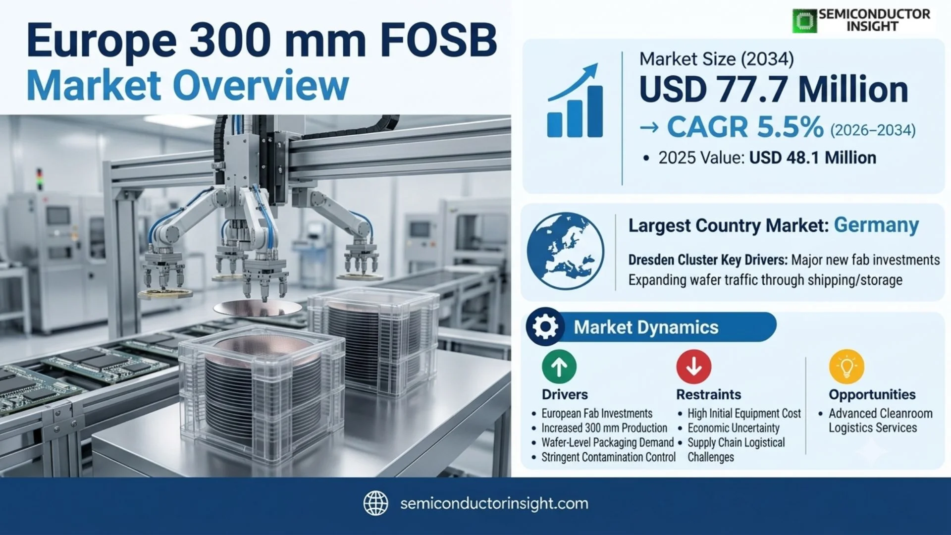
Europe 300 mm Front Opening Shipping Box (FOSB) market is rebased to USD 48.1 million in 2025 and is projected to reach USD 77.7 million by 2034, representing a 5.5% CAGR during 2026–2034. Germany is the largest country market within the report scope because the Dresden cluster combines established 300 mm production with major new fab investments that expand the number of wafers moving through shipping and storage cycles.
A 300 mm Front Opening Shipping Box is a reusable semiconductor wafer carrier designed to protect bare 300 mm wafers during transport and longer-term storage outside the controlled process flow of a wafer fab. It differs from a simple protective carton because the carrier must hold each wafer without edge or surface damage, limit contamination, maintain a secure door interface and support automated or semi-automated handling. Entegris specifies its SB300 full-pitch FOSB for 25 wafers and identifies clean, secure wafer handling, contamination minimization and reliable automation interoperability as primary applications.
Market demand is driven by physical wafer movements rather than semiconductor revenue alone. A 300 mm wafer can move between substrate suppliers, foundries, IDMs, R&D lines, external process partners and logistics hubs before final wafer processing or shipment. New European fabs increase this installed logistics base because each additional wafer-start stream requires qualified carriers, spares, cleaning procedures and inventory rotation. The commercial relationship is therefore tied to fab qualification and operational reliability: once a FOSB design is validated within a handling system, customers have strong incentives to preserve interface consistency.
Europe is entering a new 300 mm capacity cycle. The European Commission’s Chips Act framework aims to increase Europe’s role in semiconductor production, while major projects are being added in Germany and existing 300 mm facilities are being expanded in France and Italy. The ESMC Dresden facility is expected to produce 480,000 300 mm wafers per year at full capacity in 2029. ST is expanding 300 mm manufacturing in Crolles and Agrate, and imec operates 300 mm pilot capabilities in Belgium. These investments increase the number of wafer lots that require clean shipping, storage and cross-site logistics, directly broadening the operating base for FOSBs.
Segment Analysis: By Type
By type, the market is segmented into 13 Pcs Wafer Carrying Capacity and 25 Pcs Wafer Carrying Capacity. The 25-piece format is the main high-volume production configuration because it aligns with full-lot semiconductor logistics, while 13-piece carriers address engineering, partial-lot, sampling and specialized shipment requirements where customers want lower wafer count without compromising 300 mm carrier cleanliness and handling compatibility.
| Type | Operational role | Market position and purchasing logic |
|---|---|---|
| 13 Pcs Wafer Carrying Capacity | A 13-piece FOSB supports partial lots, engineering wafers, qualification samples, short process splits and shipments where a full 25-wafer load would create unnecessary inventory exposure. The smaller load does not reduce cleanliness requirements: wafer restraint, door sealing, electrostatic behavior and mechanical protection remain critical because a single damaged or contaminated 300 mm wafer can carry substantial process value after multiple fabrication steps. | The format serves a smaller but strategically important portion of the market. Demand is strongest in R&D, pilot lines, engineering changes and inter-site sample movement rather than continuous high-volume production. Suppliers compete through carrier compatibility, availability and validated cleaning or reuse procedures. Customers are less sensitive to container price than to the risk that a partial-lot shipment is delayed or compromised during a development run that may gate process qualification or a new product introduction. |
| 25 Pcs Wafer Carrying Capacity | A 25-piece FOSB is designed around the full 300 mm wafer-lot workflow used in high-volume manufacturing and commercial wafer shipping. Entegris specifies its SB300 full-pitch FOSB for 25 wafers and 300 mm wafer size, with polycarbonate structural components, a defined pitch and an automation-compatible interface. Full-lot carriers maximize shipping efficiency and simplify lot identity, storage and handling across external logistics and fab receiving operations. | This is the principal volume format because 300 mm fabs are optimized around full-lot material movement. As European wafer capacity expands, the installed base of 25-wafer shipping carriers, spares and replacements rises with it. Purchasing decisions emphasize contamination performance, door and latch reliability, wafer restraint, dimensional compatibility and lifecycle durability. Reusability means suppliers must support cleaning, inspection and replacement components, creating a service opportunity beyond the initial carrier sale. |
Carrier specification and lifecycle economics
FOSB economics are determined by lifetime performance rather than the purchase price of one box. A reusable carrier can complete many logistics cycles, so a failure that contaminates wafers, damages an edge or creates an automation stoppage can cost far more than the carrier itself. Entegris specifies polycarbonate for the shell, door and several exterior components of its SB300, with a 25-wafer capacity and a full-loaded weight of 7.8 kg. These details show why polymer cleanliness, dimensional stability, door sealing and wafer-restraint design are central to value. The supplier must maintain those characteristics after repeated handling, transport, cleaning and storage cycles.
Segment Analysis: By Application
By application, the market is segmented into IDM and Foundry. IDMs use FOSBs across internal and external wafer movements while controlling long product lifecycles, whereas foundries operate high-throughput multi-customer environments in which standardized carrier compatibility, traceability and logistics efficiency are especially important. Both applications demand stringent contamination control because a carrier can interact with high-value wafers at multiple processing stages.
| Application | Demand characteristics and commercial implication |
|---|---|
| IDM | Integrated device manufacturers control product design and manufacturing and may move wafers among internal fabs, specialty process sites, external partners, test locations and storage facilities. FOSB demand grows when an IDM adds 300 mm capacity or increases cross-site specialization. The purchasing decision emphasizes long-term supply continuity, compatibility with existing automation and cleaning procedures, and the ability to qualify one carrier design across multiple facilities. Automotive and industrial IDMs also value traceability because product programs can remain in production for many years. |
| Foundry | Foundries process wafers for many customers and operate tightly controlled, high-throughput logistics systems. The FOSB must therefore integrate predictably with receiving, stocking and automated material-handling interfaces while protecting wafers that may carry different process histories and ownership. New open-foundry capacity in Europe, including the planned ESMC Dresden facility, broadens this demand base. Foundry buyers place particular emphasis on standardized carrier geometry, low contamination, spare availability and lot traceability because a carrier issue can affect multiple customer programs and disrupt fab cycle time. |
Regional Analysis
Germany is the largest country market for 300 mm FOSBs in the report scope because Dresden is receiving the largest concentration of new 300 mm manufacturing investment. France and Italy also have substantial 300 mm capacity through ST and partner programs, Belgium is important through imec’s 300 mm R&D infrastructure, and the Netherlands, United Kingdom and Spain contribute equipment, research, design and semiconductor-ecosystem demand with lower direct wafer-production intensity.
How does FOSB demand differ across the seven European countries in the report scope?
Country demand is best understood through actual 300 mm wafer activity, because FOSBs are consumed by the logistics of wafers rather than by general electronics sales. Germany has the strongest near-term capacity additions: the European Commission says ESMC’s Dresden open foundry is expected to produce 480,000 300 mm wafers per year at full capacity in 2029, and Infineon opened a €5 billion 300 mm Smart Power Fab in Dresden in July 2026. France and Italy are scaling 300 mm facilities at Crolles and Agrate, while Belgium’s imec operates advanced 300 mm pilot lines.
| Country | Market position | Growth outlook | Demand profile | Key evidence / access factor |
|---|---|---|---|---|
| Germany | Largest | Strongest near-term expansion | High-volume fab and foundry led | ESMC is designed for 480,000 300 mm wafers per year at full capacity in 2029; Infineon opened its €5 billion 300 mm Smart Power Fab in Dresden in July 2026. |
| France | Major 300 mm production market | Strong | IDM and foundry expansion led | ST and GlobalFoundries announced a Crolles 300 mm manufacturing project targeted at up to 620,000 wafers per year at full build-out, adding substantial carrier logistics demand. |
| Italy | Major expanding production market | Strong | Smart-power and mixed-signal fab led | ST is scaling its Agrate 300 mm fab as a flagship high-volume facility and has targeted 4,000 wafers per week by 2027 before further modular expansion. |
| Belgium | Advanced R&D and pilot-line market | Steady to strong | R&D and process-development led | imec uses a 300 mm CMOS pilot line and launched a 300 mm GaN program in 2025, creating recurring demand for qualified engineering-lot and cross-partner wafer transport. |
| Netherlands | Equipment and semiconductor-ecosystem market | Steady | Equipment, R&D and logistics led | The Netherlands is central to semiconductor equipment and process-development ecosystems, but has less high-volume 300 mm wafer output than Germany, France or Italy, so FOSB demand is more qualification and logistics oriented. |
| United Kingdom | Design, compound and R&D focused | Moderate | R&D and specialty semiconductor led | The UK strategy emphasizes design, IP, compound semiconductors and R&D; it states that the country does not have a significant share of global silicon semiconductor manufacturing, limiting high-volume 300 mm FOSB consumption. |
| Spain | Developing ecosystem market | Emerging | Research, design and investment led | Spain’s PERTE Chip program was funded with €12.25 billion through 2026 to strengthen microelectronics research, design, process technology, testing and packaging, supporting ecosystem demand while high-volume 300 mm production remains limited. |
Key Europe 300 mm Front Opening Shipping Box (FOSB) Manufacturers and Competitive Landscape
The competitive landscape requires a distinction between direct wafer-carrier suppliers and the broader semiconductor-equipment companies listed on the source page. Entegris is a verified direct supplier of 300 mm FOSBs, while several other profiled companies are primarily equipment, automation, process or technology suppliers within the semiconductor ecosystem. The complete source-page company list is retained for scope fidelity, but direct FOSB competition should be assessed on actual carrier products, contamination control, automation compatibility and lifecycle support.
Entegris provides a clear reference for the product class through its SB300 full-pitch FOSB. The product is specified for 25 300 mm wafers and uses polycarbonate for the shell, door and multiple exterior components. The company positions it for wafer handling and transport, clean and secure handling, contamination minimization and reliable automation interoperability. These attributes define the competitive baseline: a FOSB supplier must control polymer materials, molding, assembly, sealing, wafer restraint and dimensional interfaces as a semiconductor contamination-control product rather than a general logistics container.
The source-page profile also includes ASML, Applied Materials, ASM International, Tokyo Electron, Lam Research and KLA. These companies are major semiconductor-equipment suppliers, but they are not treated here as direct FOSB manufacturers solely because they appear in the profiled list. Their relevance is as ecosystem participants whose equipment, process development and fab installations increase 300 mm wafer movements and impose automation-interface requirements. This distinction prevents the competitive section from overstating the direct supplier base while preserving the report’s original company scope.
Competitive advantage in FOSBs is durable because qualification is operationally sticky. A fab validates carrier dimensions, door operation, wafer restraint, particle behavior, cleaning procedures and interactions with automation or receiving tools. Once a design is embedded in those procedures, changing suppliers can require extensive requalification. Direct suppliers therefore compete through low defect rates, consistent polymer quality, documented specifications, local spares and service, and the ability to support reusable carrier fleets over many shipping cycles.
Tier structure
| Competitive tier | Representative companies | How they compete |
|---|---|---|
| Verified direct FOSB supplier | Entegris, Inc. | Competes through a documented 300 mm FOSB portfolio, polymer and wafer-contact design, contamination control, automation interoperability, replacement parts and semiconductor-grade support. Product specifications such as 25-wafer capacity, wafer pitch and dimensional tolerances are directly tied to fab logistics and carrier qualification. |
| Semiconductor equipment and process ecosystem | ASML Holding N.V.; Applied Materials, Inc.; ASM International; Tokyo Electron Limited; Lam Research Corporation; KLA Corporation | These companies influence the 300 mm operating environment through lithography, deposition, etch, inspection and metrology equipment. Their expansion in European fabs increases wafer movement and automation complexity, but their presence in the source-page company list does not by itself establish them as direct manufacturers of FOSBs. |
| Automation, laboratory and industrial ecosystem | Plastic Omnium; Thermo Fisher Scientific Inc.; Brooks Automation | These organizations participate in broader materials, laboratory, automation or industrial supply chains. Their relevance to FOSB demand is indirect unless a specific qualified wafer-carrier product is documented. The market should therefore separate direct carrier revenue from adjacent automation or materials activity when evaluating competition. |
Key companies profiled
ASML Holding N.V., Applied Materials, Inc., ASM International, Tokyo Electron Limited, Lam Research Corporation, KLA Corporation, Plastic Omnium, Thermo Fisher Scientific Inc., Brooks Automation, Entegris, Inc..
Europe 300 mm Front Opening Shipping Box (FOSB) Production Capacity Analysis
FOSB production capacity depends on precision polymer molding, clean assembly, dimensional inspection, door and latch assembly, wafer-retainer quality and contamination-controlled packaging. The limiting factor is not simply the number of injection-molding machines; suppliers must prove that each production lot maintains semiconductor-grade cleanliness, mechanical repeatability and automation compatibility after repeated shipping and cleaning cycles.
Production begins with qualified polymers and engineered components that must balance stiffness, impact resistance, dimensional stability and low contamination. Entegris specifies polycarbonate for the SB300 shell, door, door cushion and several exterior components, while the rear retainer uses polybutylene terephthalate. These material choices demonstrate why the upstream supply chain is specialized: a carrier supplier must manage resin formulation, molding conditions and component cleanliness in addition to conventional mechanical tolerances.
Assembly capacity includes door mechanisms, retainers, filters, gaskets, handles and identification features that need repeatable fit. A FOSB is expected to protect wafers while interfacing with transport and automated handling, so a dimensional deviation can create equipment faults or wafer contact. Suppliers need metrology and functional testing that verify the completed carrier rather than only molded subcomponents. The reuse model also creates aftermarket demand for replacement kits, inspection and fleet maintenance rather than a one-time container sale.
Europe’s manufacturing expansion increases demand for qualified carrier fleets, but the rate of FOSB capacity growth will not match wafer capacity one-for-one because carriers are reused. New fabs create an initial fleet requirement followed by spares, replacement and cleaning rotation. The commercial value therefore depends on wafer throughput, cross-site shipping frequency, carrier lifetime and fab inventory policy. A foundry exchanging wafers with many customers can require a different fleet size and logistics profile from an IDM with more internalized wafer flows.
| Capacity element | Technical requirement | Market implication |
|---|---|---|
| Precision polymer molding | Shell, door and structural components must maintain tight geometry, smooth wafer-protection surfaces and stable material behavior. Resin quality and molding conditions can influence particle generation, warpage and long-run dimensional consistency. | Carrier suppliers need dedicated process control and semiconductor-grade material management. Molding capacity that cannot demonstrate cleanliness and dimensional repeatability is not directly substitutable for qualified FOSB capacity, creating a higher entry barrier than general industrial plastic containers. |
| Clean assembly and inspection | Doors, wafer retainers, filters, gaskets and automation-interface features must be assembled without introducing contamination. Completed carriers require dimensional and functional inspection, not only part-level quality checks. | Inspection and traceability add cost but reduce wafer-loss risk. Customers value consistent lots and rapid root-cause support because a single carrier defect can affect high-value wafers and disrupt an automated logistics flow. |
| Reuse and service infrastructure | FOSBs are cleaned, inspected and reused across multiple shipping cycles. Replacement components and validated cleaning procedures extend fleet life while preserving contamination performance. | Suppliers can capture recurring value through replacement kits, technical support and fleet-standardization programs. A durable installed base also raises switching costs because operational procedures and automation may be optimized around one qualified carrier family. |
Europe 300 mm Front Opening Shipping Box (FOSB) Market Dynamics: Drivers, Restraints and Opportunities
The Europe 300 mm FOSB market grows with wafer-fab expansion, cross-site semiconductor logistics and the need to maintain contamination-free 300 mm wafers outside the process tool environment. Growth is moderated by carrier reuse, long qualification cycles and the concentration of high-volume wafer production in a limited number of countries. The strongest opportunity is to serve new and expanded 300 mm fabs with qualified carrier fleets, automation-compatible designs and lifecycle support rather than treating FOSBs as disposable shipping packaging.
MARKET DRIVERS
Drivers Impact Analysis*
| Factor | Direction / Intensity* | Commercial transmission mechanism |
|---|---|---|
| New European 300 mm fab capacity | High | Germany, France and Italy are adding or scaling 300 mm production, creating new wafer logistics flows and initial carrier-fleet requirements. |
| Cross-site wafer logistics and foundry activity | High | More external and multi-site wafer movements increase the number of qualified shipping carriers required per wafer-start stream. |
| Automation and contamination control | Medium to High | Fabs need carriers that interface predictably with automated systems while protecting wafer surfaces, supporting premium value for validated designs. |
| Semiconductor supply-chain localization | Medium | European policy and investment programs increase regional wafer activity and make local service, carrier availability and logistics resilience more important. |
Germany is adding major 300 mm wafer capacity
The ESMC Dresden open-foundry project is expected by the European Commission to produce 480,000 300 mm wafers per year at full capacity in 2029, and Infineon opened its €5 billion Smart Power Fab in Dresden in July 2026. Each capacity addition creates a new population of wafer lots that must be stored, transferred, shipped to partners or received from external suppliers. FOSB demand begins with the initial carrier fleet and continues through spares, replacement and reusable fleet rotation as wafer throughput increases.
France and Italy are scaling 300 mm manufacturing corridors
ST is expanding 300 mm capacity in Crolles, France, and Agrate, Italy. The Crolles project with GlobalFoundries was designed for up to 620,000 300 mm wafers per year at full build-out, while Agrate is being scaled toward 4,000 wafers per week by 2027. These manufacturing programs widen Europe’s physical 300 mm wafer base and increase inter-site material flows. Carrier suppliers benefit when they qualify designs across multiple fabs because the same FOSB family can support incoming substrates, engineering splits and external customer or partner shipments.
Contamination risk protects the value of qualified carriers
A 300 mm wafer can carry substantial value after multiple fabrication steps, so shipping risk is asymmetric: a low-cost carrier failure can damage or contaminate wafers worth many times the container. This encourages fabs to prioritize proven materials, wafer restraint, sealing and cleanliness over the lowest purchase price. Entegris positions the SB300 around clean and secure wafer handling and contamination minimization, showing how product value is linked to manufacturing yield protection rather than ordinary packaging economics.
European supply-chain resilience increases local inventory needs
The European Chips Act and national semiconductor programs are intended to strengthen regional production and supply-chain resilience. As more wafer manufacturing occurs in Europe, fabs and logistics providers need qualified carrier inventories closer to production sites to avoid delays from long-distance equipment and spare supply. This can support regional distribution, service and refurbishment activity even when the FOSBs themselves are manufactured elsewhere, increasing the commercial importance of local availability and lifecycle support.
MARKET RESTRAINTS
Restraints Impact Analysis*
| Factor | Direction / Intensity* | Commercial transmission mechanism |
|---|---|---|
| Reusable carrier economics | High | FOSBs are reused many times, so wafer-capacity growth does not translate directly into equivalent unit growth in new carriers after the initial fleet is installed. |
| Qualification and interoperability burden | High | A new carrier must work with doors, handling interfaces, cleaning procedures and automation; requalification slows supplier switching and product introductions. |
| Concentrated 300 mm production base | Medium | High-volume demand is concentrated in Germany, France and Italy, limiting the immediate market size in countries focused on design, equipment or R&D. |
| Polymer and component quality requirements | Medium | Semiconductor-grade resin, filters, seals and precision components raise manufacturing and validation cost compared with general industrial containers. |
FOSBs are reusable assets rather than consumables
A carrier can complete many shipping and storage cycles, so a fab does not need to purchase a new FOSB for every wafer lot. This limits the direct conversion of wafer-start growth into carrier-unit growth after the initial fleet has been installed. Suppliers therefore depend on new fab starts, fleet expansion, replacement of worn or damaged carriers and changes in logistics patterns. Long product life is positive for customer economics but creates a slower recurring replacement cycle than disposable semiconductor packaging materials.
Automation compatibility raises the cost of switching
FOSBs interact with loading stations, transport equipment, storage systems and operator procedures. Even when two carriers nominally fit a 300 mm wafer, differences in door behavior, dimensions, identification features or handling can require testing before a fab adopts a new design. This creates a strong incumbent advantage but also slows market entry for new suppliers. Customers may prefer a higher-priced qualified carrier rather than risk a logistics interruption that affects tool utilization or wafer cycle time.
High-volume demand remains geographically concentrated
Germany, France and Italy account for the strongest direct 300 mm manufacturing activity among the seven countries in the report scope. The Netherlands, United Kingdom, Spain and Belgium are important to equipment, R&D, design or pilot production but do not all operate comparable high-volume wafer bases. This concentration limits broad country-level scale and means suppliers must align service resources with a small number of major fab clusters rather than assuming uniform European demand.
Contamination-control specifications increase manufacturing cost
Semiconductor carriers need carefully controlled polymers, clean assembly, filtration or sealing features and dimensional inspection. These requirements increase cost relative to ordinary shipping containers and can constrain the number of qualified manufacturing lines. Recycled or lower-cost materials cannot be introduced casually because outgassing, particles or dimensional drift could affect wafers. Sustainability initiatives therefore need to preserve semiconductor cleanliness and mechanical performance, which can lengthen material-validation programs and delay cost reductions.
MARKET OPPORTUNITIES
Initial fleet build-out for new Dresden fabs
Germany offers the clearest near-term fleet opportunity because both ESMC and Infineon are expanding 300 mm manufacturing in Dresden. A new fab needs carriers before high-volume ramp, creating demand for qualification lots, initial fleets, spares and cleaning rotation. Suppliers that engage during automation and logistics commissioning can become embedded in operating procedures before full wafer volume is reached. That early qualification can support recurring replacement and service revenue once the facility reaches higher utilization.
Cross-fab standardization in France and Italy
ST is expanding 300 mm operations in Crolles and Agrate, creating an opportunity to standardize carrier families across related manufacturing sites. A supplier that can meet common automation, cleanliness and logistics requirements may reduce inventory complexity for the customer while increasing its own share of wallet. The commercial value extends beyond one FOSB sale because common replacement parts, cleaning procedures and qualification documentation can be reused across sites, making lifecycle support a competitive differentiator.
Engineering-lot carriers for Belgium and European R&D networks
imec’s 300 mm pilot line and new 300 mm GaN program create a specialized market for engineering wafers that move between equipment partners, material suppliers and research programs. Partial-lot and full-lot FOSBs are valuable in this environment because wafers can represent unique development experiments rather than high-volume product. Suppliers can differentiate through flexible quantities, rapid support and validated cleaning, capturing higher service value even when absolute carrier volumes are smaller than in a production fab.
Reusable and serviceable carrier platforms
Sustainability pressure creates an opportunity to extend carrier life through replaceable components, validated cleaning and inspection programs rather than simply introducing unqualified recycled materials. Entegris already provides replacement kits and documentation around its SB300 family. Suppliers that can quantify carrier condition and maintain contamination performance over more cycles can lower total cost for fabs while creating recurring service and parts revenue. This model aligns environmental goals with the operational need to protect expensive 300 mm wafers.
Europe 300 mm Front Opening Shipping Box (FOSB) Supply Chain Analysis
Value capture is concentrated in contamination control and qualification rather than raw polymer cost. A FOSB contains molded plastic and mechanical components, but the commercial product is a validated wafer-handling system. Material selection, molding cleanliness, door mechanics, wafer restraint, dimensional repeatability and automation compatibility must work together. This integration explains why a general industrial container manufacturer cannot enter the market simply by matching external dimensions. Customers purchase reduced wafer risk and predictable logistics behavior, which supports a specialized supplier base and long qualification relationships.
The main bottleneck is the availability of qualified carriers and service during fab ramp. New 300 mm production lines can add wafer starts faster than a carrier supplier can complete customer-specific qualification if engagement begins too late. Local stock, spare parts, technical support and cleaning or refurbishment networks therefore become strategically important around clusters such as Dresden, Crolles and Agrate. Over time, fleet utilization and carrier lifetime determine replacement demand, making operational data and preventive inspection useful tools for suppliers seeking recurring revenue after the initial fab build-out.
Recent Developments in the Europe 300 mm Front Opening Shipping Box (FOSB) Market
Infineon opened the new Dresden Smart Power Fab with a €5 billion investment and 1,000 direct jobs. The company describes the facility as a highly advanced and flexible 300 mm manufacturing site. The opening is significant for the FOSB market because a new high-volume wafer stream requires qualified shipping and storage carriers, spares and logistics processes as production ramps, expanding the installed base of 300 mm carrier fleets in Germany.
imec launched a 300 mm GaN program with initial partners including AIXTRON, GlobalFoundries, KLA, Synopsys and Veeco. The program adds another class of engineering wafers to imec’s 300 mm pilot environment and increases cross-partner development activity. For FOSB suppliers, research programs create specialized demand for secure transport of high-value engineering wafers between tool, material and device partners even when lot volumes are below those of a production foundry.
The European Commission approved a €5 billion German State-aid measure supporting ESMC’s new Dresden open foundry. The facility is designed for 300 mm silicon wafers at 28/22 nm and 16/12 nm and is expected to produce 480,000 wafers per year at full capacity in 2029. This creates a large new European wafer-logistics node and a direct future requirement for qualified 300 mm shipping carriers and reusable carrier inventory.
REPORT SCOPE & SEGMENTATION
| Attribute | Coverage |
|---|---|
| Market | Europe 300 mm Front Opening Shipping Box (FOSB) |
| Base year / forecast | 2025 base; 2026 estimate; 2034 forecast; 5.5% CAGR for 2026–2034 |
| By Type | 13 Pcs Wafer Carrying Capacity, 25 Pcs Wafer Carrying Capacity |
| By Application | IDM, Foundry |
| By Country | Germany, United Kingdom, France, Italy, Spain, Netherlands, Belgium |
| Companies profiled | ASML Holding N.V., Applied Materials, Inc., ASM International, Tokyo Electron Limited, Lam Research Corporation, KLA Corporation, Plastic Omnium, Thermo Fisher Scientific Inc., Brooks Automation, Entegris, Inc. |
Frequently Asked Questions
What is the Europe 300 mm Front Opening Shipping Box (FOSB) market size?
The Europe 300 mm Front Opening Shipping Box (FOSB) market is valued at USD 48.1 million in 2025 and is projected to reach USD 77.7 million by 2034, representing a 5.5% CAGR during 2026–2034. Growth is supported by new and expanded 300 mm wafer manufacturing in Germany, France and Italy, as well as R&D activity in Belgium. Reusable carrier economics and lengthy qualification cycles keep growth steadier than the underlying increase in wafer-fab capital spending.
Which country is the largest market for 300 mm FOSBs in Europe?
Germany is the largest country market in 2025 within the report scope. Dresden already has a major semiconductor cluster and is adding new 300 mm capacity. The ESMC open foundry is expected to produce 480,000 300 mm wafers per year at full capacity in 2029, while Infineon opened its €5 billion Smart Power Fab in July 2026. These investments create significant initial carrier-fleet, spare, cleaning and replacement requirements as wafer throughput ramps.
What is a 300 mm FOSB used for?
A 300 mm FOSB is a reusable carrier for shipping and longer-term storage of bare 300 mm semiconductor wafers outside the controlled wafer-processing sequence. It protects wafers against mechanical contact and contamination while providing a standardized front-opening interface for handling. Entegris specifies its SB300 FOSB for 25 wafers and highlights clean, secure handling and automation interoperability. The carrier is therefore part of semiconductor contamination control and fab logistics, not simply protective packaging.
Which FOSB carrying capacity is most important?
The 25 Pcs Wafer Carrying Capacity format is the principal high-volume configuration because it aligns with a full 300 mm wafer lot and maximizes logistics efficiency. The 13-piece format remains important for engineering samples, process splits and partial-lot shipments. Both require the same core cleanliness and mechanical protections. The commercial difference is utilization: full-lot carriers are tied to production throughput, while smaller-capacity carriers are weighted toward R&D and qualification flows.
Which applications drive the FOSB market?
The report segments demand into IDM and Foundry applications. IDMs use FOSBs for internal and external movements across their manufacturing networks, often with long product lifecycles and strict traceability. Foundries operate multi-customer, high-throughput environments and need standardized carrier compatibility, contamination control and automation reliability. The ESMC project in Dresden is particularly relevant because it will operate as an open foundry, creating a new European wafer-logistics node serving multiple customers and process flows.
Why do FOSB qualification cycles create supplier stickiness?
A FOSB interacts with wafers, loading and unloading procedures, doors, storage, transport equipment and sometimes automated handling interfaces. Customers therefore validate carrier dimensions, door behavior, wafer restraint, cleanliness and cleaning procedures before production use. Changing to another design can require repeated compatibility testing and operational documentation. This gives qualified suppliers a durable position but also raises the market-entry barrier for new vendors, because matching outer dimensions alone is insufficient to prove semiconductor-grade reliability.
How does the expansion of European 300 mm fabs affect FOSB demand?
New fabs create an initial need for qualified carrier fleets before wafer volume reaches full production. Germany is adding ESMC and Infineon capacity, while ST is expanding 300 mm manufacturing in Crolles, France, and Agrate, Italy. As each site ramps, carriers are needed for incoming substrates, engineering lots, inter-site movements, customer shipments, spares and cleaning rotation. Because FOSBs are reusable, replacement demand then depends on carrier life, utilization, damage rates and logistics intensity rather than on one new carrier per wafer lot.
Who is a verified direct supplier in the report’s competitive set?
Entegris, Inc. is a verified direct supplier through its documented SB300 full-pitch 300 mm FOSB product. The source-page company list also includes major semiconductor-equipment and automation companies, but their presence in the list does not by itself establish them as FOSB manufacturers. The competitive analysis therefore retains all profiled names for scope fidelity while distinguishing direct carrier products from adjacent equipment, automation, laboratory and semiconductor-ecosystem activity.
What materials are used in a 300 mm FOSB?
Entegris specifies polycarbonate for the shell, door, door cushion and several exterior elements of its SB300 FOSB, with polybutylene terephthalate used for the rear retainer and a thermoplastic elastomer gasket. These materials must maintain dimensional stability and cleanliness through repeated use. The key commercial issue is not the polymer name alone; molding, assembly, filtration, sealing and cleaning must prevent particle generation and protect wafer surfaces over many transport and storage cycles.
What is the strongest opportunity through 2034?
The strongest opportunity is to become the qualified carrier platform for new and expanded 300 mm fabs during their commissioning and ramp. Early engagement allows a supplier to validate dimensions, automation interfaces, cleaning procedures and fleet-management practices before full production begins. Germany offers the clearest near-term opportunity, while France and Italy provide substantial ongoing expansion. A second opportunity exists in reusable-carrier services, replacement components and fleet inspection, which can generate recurring value after the initial carrier inventory has been purchased.
Research Sources & Evidence Base
View research sources used for this overview.
- Entegris. SB300 Full Pitch Front Opening Shipping Boxes (FOSBs), direct FOSB product specifications, 25-wafer capacity, 300 mm wafer size, materials and handling applications.
- European Commission. Chips Act, European semiconductor production and supply-chain policy context.
- European Commission. Commission approves €5 billion German State aid measure to support ESMC, ESMC Dresden 300 mm technology, 480,000-wafer annual full-capacity target and 2029 timing.
- Infineon Technologies. Infineon opens the Smart Power Fab in Dresden, €5 billion Dresden fab opening and 1,000 direct jobs, 2 July 2026.
- STMicroelectronics. Manufacturing strategic programs, 300 mm capacity expansion in Crolles, France, and Agrate, Italy.
- STMicroelectronics. ST and GlobalFoundries to advance FD-SOI ecosystem with new 300mm manufacturing facility in France, Crolles 300 mm project and up to 620,000 wafers per year at full build-out.
- imec. imec launches 300mm GaN program, Belgian 300 mm pilot-line and power-electronics development activity, 6 October 2025.
- UK Government. National semiconductor strategy, UK semiconductor focus, funding commitments and limited share of global silicon manufacturing.
- European Commission Representation in Spain. PERTE Chip, €12.25 billion of European funds, Spanish semiconductor research, design, process, test and packaging investment context.
Get Sample Report PDF for Exclusive Insights
Report Sample Includes
- Table of Contents
- List of Tables & Figures
- Charts, Research Methodology, and more...
 Download Sample Report PDF