
Market Insights
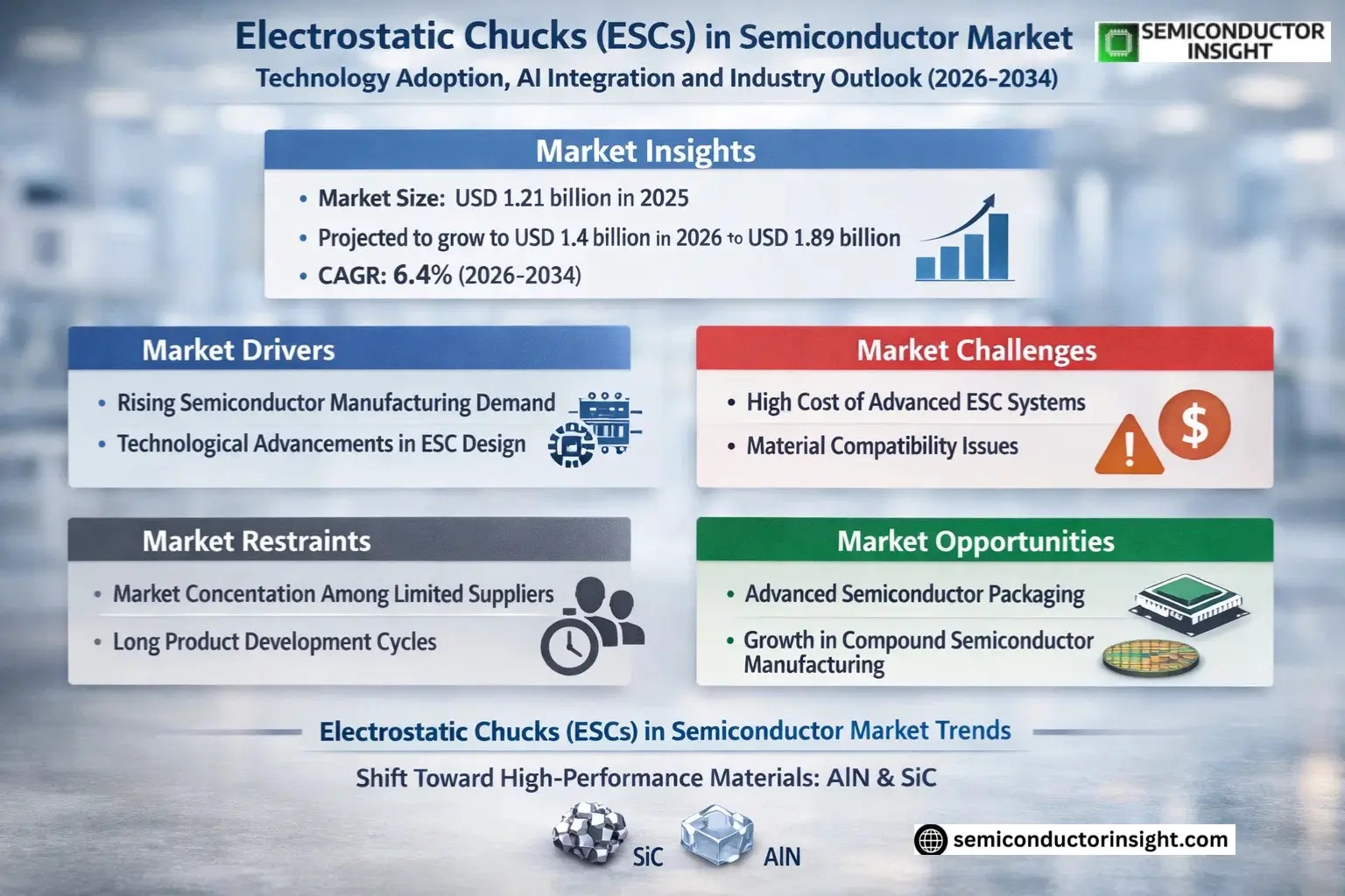
Global Electrostatic Chucks (ESCs) in Semiconductor Market size was valued at USD 1.21 billion in 2025. The market is projected to grow from USD 1.29 billion in 2026 to USD 1.89 billion by 2034, exhibiting a CAGR of 6.4% during the forecast period.
Electrostatic Chucks (ESCs) are critical components used in semiconductor manufacturing equipment to securely hold silicon wafers during processes like etching, deposition, and ion implantation. These devices utilize electrostatic force for wafer clamping, eliminating mechanical stress while ensuring precise positioning and thermal management. Key materials used in ESCs include alumina, aluminum nitride, and silicon carbide, which offer high thermal conductivity and electrical insulation properties required for advanced semiconductor fabrication.
The market growth is driven by increasing investments in semiconductor manufacturing capacity expansion and the transition to smaller process nodes below 7nm, which demand higher precision wafer handling solutions. While the industry faces challenges from supply chain complexities and material cost fluctuations, technological advancements in chuck design and the rising adoption of 300mm wafers continue to create new opportunities. Leading manufacturers are focusing on developing multi-electrode ESCs with enhanced temperature control capabilities to meet evolving industry requirements.
MARKET DRIVERS
Increasing Semiconductor Manufacturing Demand
The growing adoption of advanced semiconductor manufacturing processes is driving demand for precision wafer handling solutions like Electrostatic Chucks (ESCs). With semiconductor fabrication plants expanding globally, the need for high-performance ESCs has surged by approximately 18% annually over the past three years.
Technological Advancements in ESC Design
Modern ESCs now incorporate advanced materials and innovative electrostatic designs that improve heat dissipation and wafer stability. The development of bipolar ESCs has enabled higher throughput in semiconductor manufacturing, reducing production costs by an estimated 12-15% per wafer.
Miniaturization trends in semiconductor devices below 7nm nodes are creating additional demand for ultra-precise ESCs with sub-micron accuracy.
MARKET CHALLENGES
High Cost of Advanced ESC Systems
Coulomb-type and Johnsen-Rahbek ESCs for advanced semiconductor nodes can cost upwards of USD 20,000 per unit, creating significant capital expenditure challenges for smaller manufacturers. Maintenance and replacement costs add approximately 30% to the total cost of ownership.
Other Challenges
Material Compatibility Issues
Development of ESC materials compatible with new semiconductor processes remains challenging, particularly for gallium nitride and silicon carbide wafer applications.
Technical Complexity in ESC Manufacturing
The precision manufacturing requirements for semiconductor-grade ESCs limit production to a handful of specialized manufacturers, creating supply chain vulnerabilities.
MARKET RESTRAINTS
Market Concentration Among Limited Suppliers
Electrostatic Chucks (ESCs) in Semiconductor Market is dominated by three major suppliers controlling approximately 75% of global capacity. This oligopoly creates pricing pressures and limits technological innovation in certain segments of the market.
Long Product Development Cycles
Developing new ESC models for specific semiconductor applications typically requires 18-24 months of R&D and testing, slowing the pace of market expansion and technology adoption.
MARKET OPPORTUNITIES
Emerging Applications in Advanced Packaging
The rapid growth of 2.5D and 3D semiconductor packaging is creating new opportunities for specialized ESCs designed for through-silicon via (TSV) and wafer-level packaging applications.
Expansion in Compound Semiconductor Manufacturing
Increasing production of GaN and SiC power devices is driving demand for ESCs with specialized dielectric materials capable of handling higher temperatures and different wafer chemistries.
Electrostatic Chucks (ESCs) in Semiconductor Market TrendsShift Toward High-Performance Materials
Electrostatic Chucks (ESCs) in Semiconductor Market is witnessing increased adoption of advanced materials like aluminum nitride (AlN) and silicon carbide (SiC). These materials offer superior thermal conductivity and stability compared to traditional alumina-based chucks, meeting the demands of advanced semiconductor nodes. Leading manufacturers are investing in material innovation to improve wafer temperature uniformity and reduce particle contamination risks.
Other Trends
Integration with Smart Manufacturing Systems
ESC manufacturers are incorporating IoT-enabled sensors for real-time monitoring of chuck performance metrics like temperature distribution and clamping force. This integration supports predictive maintenance and enhances process control in semiconductor fabs, reducing downtime and improving yield rates.
Expansion in 300mm Wafer Applications
With semiconductor manufacturers transitioning to larger wafer sizes, demand for 300mm-compatible ESCs has surged. The market is seeing rapid development of multi-electrode designs that provide more uniform electrostatic force distribution across larger wafer surfaces, critical for leading-edge process nodes below 7nm.
Supply Chain Localization Initiatives
Geopolitical factors are driving regional ESC supply chain development, particularly in Asia and North America. Several semiconductor equipment manufacturers are forming strategic partnerships with local ESC suppliers to ensure stable component availability and reduce lead times for critical fab equipment.
Enhanced Thermal Management Solutions
Advanced thermal control systems are being integrated into next-generation ESCs to address heat dissipation challenges in extreme semiconductor processes. New designs incorporate optimized cooling channels and temperature feedback loops to maintain precise wafer temperatures during high-power operations.
COMPETITIVE LANDSCAPE
Key Industry Players
[Strategic Positioning in the USD 1.89 Billion ESCs Market by 2034]
Electrostatic Chucks (ESCs) in Semiconductor Market is dominated by specialized material science and precision engineering companies, with Japanese firms controlling approximately 65% of global production capacity. SHINKO and NGK Insulators lead the market with vertically integrated manufacturing from ceramic substrates to finished assemblies, securing contracts with major semiconductor equipment OEMs like Applied Materials and Lam Research. The industry structure features high entry barriers due to IP protection of ceramic compositions and proprietary electrode designs requiring over 18 months of qualification cycles with chip manufacturers.
Second-tier players including TOTO, NTK CERATEC, and Sumitomo Osaka Cement compete through niche material formulations and regional partnerships, particularly in emerging 300mm wafer fabs across Asia. Emerging Chinese suppliers like Beijing U-precision Tech are gaining traction in domestic markets through government-supported semiconductor equipment localization initiatives, though still lag in high-end Coulomb-type ESC technologies as of 2025. The competitive environment is intensifying as wafer processing temperatures exceed 600°C in advanced nodes, driving R&D investments in next-generation AlN/SiC composite materials.
List of Key Electrostatic Chucks (ESCs) Companies Profiled
- SHINKO
- NGK Insulators
- TOTO
- NTK CERATEC
- Entegris
- Sumitomo Osaka Cement
- LK ENGINEERING
- MiCo
- Kyocera
- Technetics
- Creative Technology Corporation
- Krosaki Harima Corporation
- TOMOEGAWA
- Beijing U-precision Tech
- Coherent
Segment Analysis:
| Segment Category | Sub-Segments | Key Insights |
| By Type |
|
Aluminum Nitride ESCs demonstrate superior thermal conductivity and electrical insulation properties, making them ideal for high-temperature semiconductor processes:
|
| By Application |
|
300mm Wafer Processing dominates application segments with critical performance requirements:
|
| By End User |
|
Foundries represent the most demanding segment with stringent technical requirements:
|
| By Electrode Type |
|
Johnsen-Rahbek (JR) Type ESCs offer significant operational advantages for semiconductor manufacturing:
|
| By Process Application |
|
Etching Processes demand the most sophisticated ESC solutions:
|
Regional Analysis: Electrostatic Chucks (ESCs) in Semiconductor Market
Asia-Pacific
Taiwan’s Foundry Leadership
Taiwan’s semiconductor foundries drive ESC innovation through extreme process requirements. TSMC’s transition to 2nm processes necessitates ESCs with nano-level flatness and superior particle control. Local ESC suppliers are developing specialized coatings for advanced node compatibility, while international manufacturers establish joint ventures to meet demand.
South Korea’s Memory Focus
South Korean memory manufacturers require ESCs optimized for high-volume 3D NAND production. ESC solutions in Korea emphasize thermal uniformity for stacked architectures and compatibility with extreme aspect ratio etching. Domestic ESC developers work closely with equipment OEMs to create customized chucking solutions for DRAM scaling challenges.
China’s Capacity Expansion
China’s aggressive semiconductor self-sufficiency push creates growing ESC demand across mature and advanced nodes. Domestic ESC suppliers are improving dielectric materials and power systems to compete with international players. The government’s “Big Fund” investments accelerate localization of critical components including precision ESCs.
Japan’s Materials Expertise
Japan leads in ESC ceramic materials and advanced coatings technology. Japanese suppliers provide critical components for global ESC manufacturers while developing next-gen solutions with improved wear resistance. Collaborations between material science institutes and equipment makers drive innovations in ESC durability for harsh process environments.
North America
North America maintains strong ESC market presence through semiconductor equipment innovation and R&D leadership. U.S.-based ESC manufacturers focus on advanced designs for EUV lithography tools and atomic layer deposition systems. The region sees growing demand for AI-optimized ESCs that integrate real-time process monitoring. Major IDMs and equipment vendors collaborate on ESC solutions for gate-all-around transistor architectures, pushing the boundaries of precision and thermal management requirements.
Europe
Europe’s ESC market benefits from specialization in power semiconductor and MEMS manufacturing. German and Dutch equipment makers drive demand for ESCs capable of handling large-diameter silicon carbide wafers. Research institutions across Europe collaborate on ESC technologies for quantum computing applications, focusing on ultra-low temperature operation. The region maintains a strong position in ESC control systems and precision power supply development.
Middle East & Africa
Emerging semiconductor initiatives in the Middle East create new opportunities for ESC technology adoption. Investment in compound semiconductor manufacturing requires specialized ESCs for gallium nitride and silicon carbide processing. Partnerships with European and Asian ESC suppliers help bridge the technology gap while local universities establish research programs in wafer handling technologies.
South America
South America’s growing semiconductor packaging and test sector drives basic ESC requirements. While the region has limited front-end semiconductor manufacturing, increasing investments in assembly facilities create demand for cost-effective ESC solutions. Local suppliers focus on refurbishment and maintenance services for existing ESC installations in industrial applications.
Report Scope
This market research report provides a comprehensive analysis of the Electrostatic Chucks (ESCs) in Semiconductor Market, covering the forecast period 2025–2034. It offers detailed insights into market dynamics, technological advancements, competitive landscape, and key trends shaping the industry.
Key focus areas of the report include:
- Market Overview: The report begins with an overview outlining its current market scenario, key growth indicators, and industry transformation drivers. It discusses macroeconomic factors, demand–supply balance, regulatory landscape, and the strategic role of ESCs in semiconductor manufacturing applications such as PVD, PECVD, etching, and ion implantation.
- Market Size & Forecast: Historical data and future projections for revenue, unit shipments, and market value across major regions and segments.
- Segmentation Analysis: Detailed breakdown by product type, electrode type, structural form, application, and end-user industry to identify high-growth segments.
- Regional Insights: Insights into market performance across North America, Europe, Asia-Pacific, Latin America, and Middle East & Africa.
- Competitive Landscape: Profiles of leading market participants including SHINKO, NGK Insulators, TOTO, NTK CERATEC, and Entegris.
- Technology Trends & Innovation: Assessment of material systems, structural design advancements, and reliability validation methods.
- Market Drivers & Restraints: Evaluation of factors driving market growth along with challenges in supply chain and high-end application validation.
- Stakeholder Insights: Strategic insights for component suppliers, OEMs, and investors regarding the evolving semiconductor equipment ecosystem.
Primary and secondary research methods are employed, including interviews with industry experts and data from verified sources to ensure accuracy.
FREQUENTLY ASKED QUESTIONS:
What is the current market size of Electrostatic Chucks (ESCs) in Semiconductor Market?
-> Electrostatic Chucks (ESCs) in Semiconductor Market size was valued at USD 1.21 billion in 2025. The market is projected to grow from USD 1.29 billion in 2026 to USD 1.89 billion by 2034, exhibiting a CAGR of 6.4% during the forecast period.
What is the expected CAGR of the market?
-> The market is expected to grow at a CAGR of 6.4% during 2025-2034.
Which key companies operate in Electrostatic Chucks (ESCs) in Semiconductor Market?
-> Key players include SHINKO, NGK Insulators, TOTO, NTK CERATEC, Entegris, Sumitomo Osaka Cement, Kyocera, and Coherent.
What are the key growth drivers?
-> Key growth drivers include sustained investment in semiconductor manufacturing equipment, advanced process node requirements, and supply chain security considerations.
Which region dominates the market?
-> Asia dominates the market, with strong presence in China, Japan, and South Korea.
What are the key applications of ESCs?
-> Primary applications include 200mm and 300mm wafer processing in PVD, PECVD, etching, and ion implantation equipment.
Get Sample Report PDF for Exclusive Insights
Report Sample Includes
- Table of Contents
- List of Tables & Figures
- Charts, Research Methodology, and more...
 Download Sample Report PDF





