
EDA Tools for Digital IC Design Market Insights
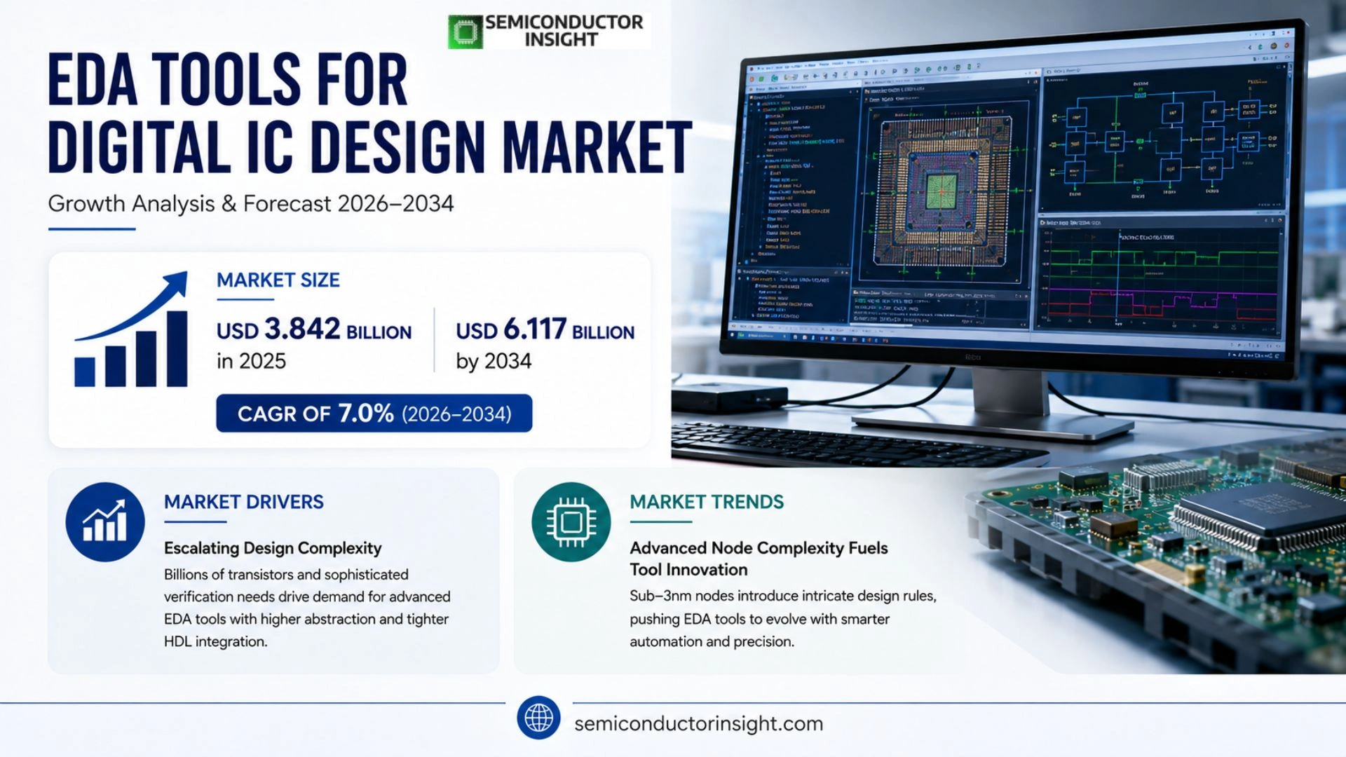
Global EDA Tools for Digital IC Design market size was valued at USD 3.842 billion in 2025 and is forecasted to reach USD 6.117 billion by 2034, reflecting a CAGR of 7.0% over the forecast horizon.
Electronic Design Automation (EDA) software supports chip creation through three core capabilities: simulation tools predict circuit behavior from a schematic before silicon fabrication; design tools translate functional descriptions into logical netlists and physical layout geometries, blending automated synthesis with interactive guidance; verification tools examine both logical and physical representations to confirm connectivity, timing closure, power budgets and reliability criteria.
The upward trajectory of the market stems from several influences including the transition to sub‑3 nm process nodes that raise design rule complexity, the surge in AI‑enabled workloads demanding custom accelerators, and the expansion of high‑performance computing, 5G/6G and autonomous vehicle applications that require sophisticated chip architectures. Companies such as Synopsys, Cadence, Siemens EDA and Silvaco have broadened their portfolios with cloud‑based offerings and subscription models to meet these demands, while recent collaborations among leading vendors aim to integrate machine‑learning‑assisted optimization into the design flow.
MARKET DRIVERS
Escalating Design Complexity
Modern semiconductor devices now incorporate billions of transistors, prompting designers to rely on sophisticated verification and synthesis capabilities. This surge in transistor count forces EDA Tools for Digital IC Design Market to deliver higher abstraction levels and tighter integration with hardware description languages, ensuring time‑to‑market remains competitive.
Shift Toward Heterogeneous Integration
Manufacturers increasingly adopt chip‑let architectures and 2.5 D/3 D packaging. Such architectures demand tools that can co‑optimize interconnects, power distribution, and thermal profiles across dissimilar blocks. Vendors that embed these functions into their suites are seeing stronger adoption rates among system‑level designers.
➤ “Design teams that integrate early‑stage power analysis report up to 15 % reduction in silicon iteration cycles.”
The industry’s emphasis on early validation translates into higher budget allocations for simulation engines capable of handling mixed‑signal corners. Consequently, firms that expand their portfolio with accurate, low‑ latency simulators are positioned to capture fresh spending streams.
MARKET CHALLENGES
Rising Licensing Costs
Premium pricing structures for flagship EDA suites compel many mid‑size design houses to evaluate total cost of ownership carefully. When licensing fees eclipse projected project margins, organizations may defer tool upgrades, slowing the diffusion of advanced capabilities.
Other Challenges
Talent Shortage
The rapid evolution of design methodologies outpaces the supply of engineers proficient in newer verification languages and AI‑augmented layout optimizers. Companies must invest heavily in training programs or risk extending development timelines.
MARKET RESTRAINTS
Intellectual Property Concerns
Design houses increasingly guard core IP behind secure repositories, limiting the extent to which third‑party tools can perform deep analysis. This protective stance can hinder tool integration and force vendors to negotiate costly access agreements.
Regulatory Compliance Overhead
Emerging standards for safety‑critical systems, such as automotive ISO 26262, impose rigorous verification checkpoints. Tools that do not natively support traceability or certification‑ready reporting face resistance from OEMs seeking to streamline compliance audits.
When combined, IP safeguards and compliance burdens create a friction layer that slows adoption of newer EDA functionalities, especially among firms operating in highly regulated verticals.
MARKET OPPORTUNITIES
AI‑Driven Design Automation
Machine‑learning models that predict routing congestion or suggest clock‑tree optimizations are moving from prototype to production. Companies that embed AI cores into their toolchains can offer designers a tangible reduction in manual iteration, unlocking new revenue streams within EDA Tools for Digital IC Design Market.
Cloud‑Based Collaborative Platforms
Distributed design teams benefit from SaaS environments that provide on‑demand compute and secure data sharing. As latency concerns diminish with edge‑cloud networks, providers that deliver scalable, subscription‑based solutions are likely to capture a growing share of design spend.
Finally, the convergence of hardware‑software co‑design, especially in the realm of emerging quantum‑compatible digital blocks, opens a niche where traditional EDA offerings can expand into new architectural territories, delivering differentiated value to forward‑looking semiconductor manufacturers.
EDA Tools for Digital IC Design Market Trends
Advanced Node Complexity Fuels Tool Innovation
The migration to sub‑3nm process nodes has introduced a lattice of design rules that exceed the capacity of legacy automation. As physical effects such as quantum tunneling and line‑edge roughness become dominant, simulation engines must predict behavior with picosecond precision, while place‑and‑route tools are required to reconcile timing, power and manufacturability in a single pass. Companies that adopt tighter integration between logical synthesis and physical implementation see a reduction in iteration loops, enabling them to meet aggressive product launch windows. For EDA Tools for Digital IC Design Market, this shift translates into higher spending on premium suites, a push for IP‑centric workflows, and an intensified focus on vendor partnerships that can deliver end‑to‑end sign‑off solutions.
Other Trends
Verification and Reliability Emphasis
Modern chips serve safety‑critical domains such as autonomous driving and medical imaging, raising the bar for proof of correctness. Verification platforms now embed machine‑learning classifiers that sift through massive stimulus sets to isolate corner cases, cutting down manual debug time. At the same time, reliability modules incorporate variation‑aware analysis to forecast yield loss under different operating conditions. The practical outcome for design houses is a tighter validation schedule, which in turn pressures tool vendors to supply out‑of‑the‑box compliance checks and customizable rule sets. This evolution reinforces the strategic importance of verification within the broader EDA Tools for Digital IC Design Market.
Shift Toward Cloud‑Based Subscription Models
Clients increasingly favor consumption‑based licensing over perpetual purchases, attracted by the ability to scale compute resources on demand. Cloud‑hosted EDA environments deliver elastic rendering power for intensive simulation tasks, while also centralizing data management across geographically dispersed teams. Vendors responding to this preference are re‑architecting their offerings to support multi‑tenant security frameworks and API‑driven integration with PLM systems. For the industry, the transition reshapes revenue streams, accelerates adoption cycles, and lowers the barrier for smaller firms to access state‑of‑the‑art design tools without large upfront capital outlays.
COMPETITIVE LANDSCAPE
Key Industry Players
Competitive dynamics in the Digital IC Design EDA Tools market
Synopsys and Cadence Design Systems dominate the upper tier of the ecosystem, accounting for a combined share that eclipses half of global revenue in 2025. Their advantage springs from end‑to‑end portfolios that span RTL synthesis, place‑and‑route, sign‑off verification and post‑silicon validation. By embedding extensive IP libraries and AI‑augmented optimization engines, they turn design turn‑around time into a differentiator for customers racing toward sub‑3 nm processes. Their licensing models,mixing perpetual cores with subscription layers,lock in long‑term relationships while providing the cash flow needed to sustain heavy R&D spend. Consequently, smaller competitors must either specialise in a narrow function or partner with these leaders to gain market exposure, shaping an oligopolistic structure where the two giants set pricing benchmarks and influence the direction of standards development.
The remainder of the field consists of firms that have carved out defensible niches through focused innovation or regional strength. Siemens EDA (formerly Mentor) commands a solid foothold in verification and advanced‑node physical‑design tools, leveraging its deep ties with major foundries. Silvaco remains the go‑to supplier for mixed‑signal and memory‑centric solutions, while Agnisys has pushed AI‑driven synthesis to the forefront of low‑power IoT chip projects. Empyrean Technology and Xpeedic differentiate themselves with cloud‑native platforms that promise rapid scalability for design teams scattered across continents. Companies such as Semitronix, Faraday Dynamics, MircoScape Technology, Primarius Technologies, Arcas‑tech, UniVista Industrial Software, Shanghai LEDA Technology and Phlexing Technology concentrate on bespoke functionalities,ranging from custom layout generators to security‑focused verification,allowing them to attract boutique customers and niche foundry programs. Their strategies,strategic alliances, targeted acquisitions, and SaaS‑first offerings,create a heterogeneous competitive set that pressures the incumbents to continuously broaden feature sets and improve cost efficiency.
List of Key EDA Tools for Digital IC Design Companies Profiled
- Synopsys
- Cadence Design Systems
- Siemens EDA
- Silvaco
- Agnisys
- Empyrean Technology
- Xpeedic
- Semitronix
- Faraday Dynamics
- MircoScape Technology
- Primarius Technologies
- Arcas-tech
- UniVista Industrial Software
- Shanghai LEDA Technology
- Phlexing Technology
Segment Analysis:
| Segment Category | Sub-Segments | Key Insights |
| By Type |
|
Simulation remains the cornerstone for early risk mitigation, enabling designers to anticipate functional behavior before silicon commitment.
|
| By Application |
|
Automotive applications drive a sophisticated blend of safety‑critical verification and power‑aware design.
|
| By End User |
|
Chip Designers seek seamless transitions from architectural exploration to physical implementation.
|
| By Deployment Mode |
|
Cloud‑based deployment is reshaping how design teams collaborate across geographies.
|
| By Business Model |
|
Subscription models are gaining traction as they provide continuous updates and support.
|
Regional Analysis: EDA Tools for Digital IC Design Market
North America
Vendors are prioritizing tighter integration with high‑performance simulation kernels to shave weeks off iterative loops, a necessity for companies racing to qualify next‑generation nodes.
Emerging machine‑learning modules embedded in synthesis tools are gaining traction, enabling designers to explore unconventional floorplans without manual trial and error.
Cloud‑based design environments that enforce granular access controls are becoming a prerequisite for multinational projects concerned about IP leakage.
Strategic alliances between EDA firms and silicon foundries are deepening, allowing toolchains to be tuned directly for specific process libraries and enhancing yield predictions.
Europe
European semiconductor hubs, notably in Germany and the Netherlands, are leveraging stringent energy‑efficiency standards to push tool developers toward low‑power optimization features. The region’s regulatory emphasis on sustainable design translates into a demand for verification suites that can model power‑grid interactions early in the flow. Moreover, a strong academic‑industry nexus fuels the incorporation of cutting‑edge formal methods, positioning Europe as a crucible for rigorous correctness guarantees. Companies operating here must reconcile tight environmental mandates with the need for rapid design closure, prompting vendors to offer modular solutions that can be tailored to diverse compliance frameworks.
Asia-Pacific
The Asia‑Pacific corridor, driven by manufacturing powerhouses in Taiwan, South Korea, and China, emphasizes throughput and scalability in its tool preferences. High‑volume fabs require design environments that can handle massive design databases without compromising performance, encouraging vendors to refine memory‑efficient algorithms. Additionally, the region’s aggressive product roadmaps demand early‑release support for emerging process nodes, compelling tool providers to adopt a forward‑looking development cadence. Cultural emphasis on cost‑effectiveness also steers customers toward flexible licensing models that align with fluctuating project pipelines.
South America
South American markets are gradually emerging from a historical reliance on imported design services toward building localized expertise. Brazil’s growing semiconductor research initiatives are prompting early‑stage adoption of comprehensive design suites that bundle layout, verification, and physical‑design capabilities. The focus here is on tools that can bridge skill gaps, offering intuitive user interfaces and robust training resources. While the overall market size remains modest, the region’s trajectory suggests increasing appetite for solutions that can accelerate knowledge transfer and reduce dependence on overseas consultancy.
Middle East & Africa
Investment in semiconductor design capabilities across the Middle East and Africa is still nascent, yet strategic government programs are nurturing a pipeline of engineering talent. Countries such as the United Arab Emirates are establishing innovation parks that attract multinational EDA vendors seeking footholds in emerging ecosystems. In this context, vendors are tailoring entry‑level toolkits that emphasize ease of integration with existing CAD infrastructures while providing scalability pathways as local design proficiency matures. The overarching narrative is one of cautious optimism, with a clear preference for solutions that can grow alongside the region’s evolving design ambitions.
Report Scope
This market research report provides a comprehensive analysis of the EDA Tools for Digital IC Design Market , covering the forecast period 2026–2034. It offers detailed insights into market dynamics, technological advancements, competitive landscape, and key trends shaping the industry.
Key focus areas of the report include:
- Market Overview: The report begins with an overview outlining its current market scenario, key growth indicators, and industry transformation drivers. It discusses macroeconomic factors, demand–supply balance, regulatory landscape, and the strategic role of semiconductors in powering advancements across industries such as automotive, telecommunications, consumer electronics, and industrial automation.
- Market Size & Forecast: Historical data and future projections for revenue, unit shipments, and market value across major regions and segments.
- Segmentation Analysis: Detailed breakdown by product type, technology, application, and end-user industry to identify high-growth segments and investment opportunities.
- Regional Insights: Insights into market performance across North America, Europe, Asia-Pacific, Latin America, and the Middle East & Africa, including country-level analysis where relevant.
- Competitive Landscape: Profiles of leading market participants, including their product offerings, R&D focus, manufacturing capacity, pricing strategies, and recent developments such as mergers, acquisitions, and partnerships.
- Technology Trends & Innovation: Assessment of emerging technologies, integration of AI/IoT, semiconductor design trends, fabrication techniques, and evolving industry standards.
- Market Drivers & Restraints: Evaluation of factors driving market growth along with challenges, supply chain constraints, regulatory issues, and market-entry barriers.
- Stakeholder Insights: Insights for component suppliers, OEMs, system integrators, investors, and policymakers regarding the evolving ecosystem and strategic opportunities.
Primary and secondary research methods are employed, including interviews with industry experts, data from verified sources, and real-time market intelligence to ensure the accuracy and reliability of the insights presented.
FREQUENTLY ASKED QUESTIONS:
What is the current market size of EDA Tools for Digital IC Design Market?
-> EDA Tools for Digital IC Design market is forecasted to reach USD 6.117 billion by 2034, reflecting a CAGR of 7.0%
Which key companies operate in EDA Tools for Digital IC Design Market?
-> Key players include Synopsys, Cadence, Siemens EDA, Silvaco, Agnisys, Empyrean Technology, Xpeedic, Semitronix, Faraday Dynamics, MircoScape Technology, Primarius Technologies, Arcas-tech, UniVista Industrial Software, Shanghai LEDA Technology, Phlexing Technology, Robei EDA, HyperSilicon, S2C, X-EPIC, Huaxin Jushu.
What are the key growth drivers?
-> Key growth drivers include advancement of sub‑3nm process nodes, increasing chip complexity, AI‑enabled design automation, rising demand for high‑performance computing, 5G/6G rollout, and autonomous‑driving applications.
Which region dominates the market?
-> Asia is the dominant region, driven by major semiconductor fabs in China, Japan, South Korea, and Taiwan, while North America remains a key innovation hub.
What are the emerging trends?
-> Emerging trends include cloud‑based EDA platforms, AI/ML‑assisted verification, increased adoption of subscription licensing models, and integration of hardware‑software co‑design workflows.

Get Sample Report PDF for Exclusive Insights
Report Sample Includes
- Table of Contents
- List of Tables & Figures
- Charts, Research Methodology, and more...
 Download Sample Report PDF