Market Insights
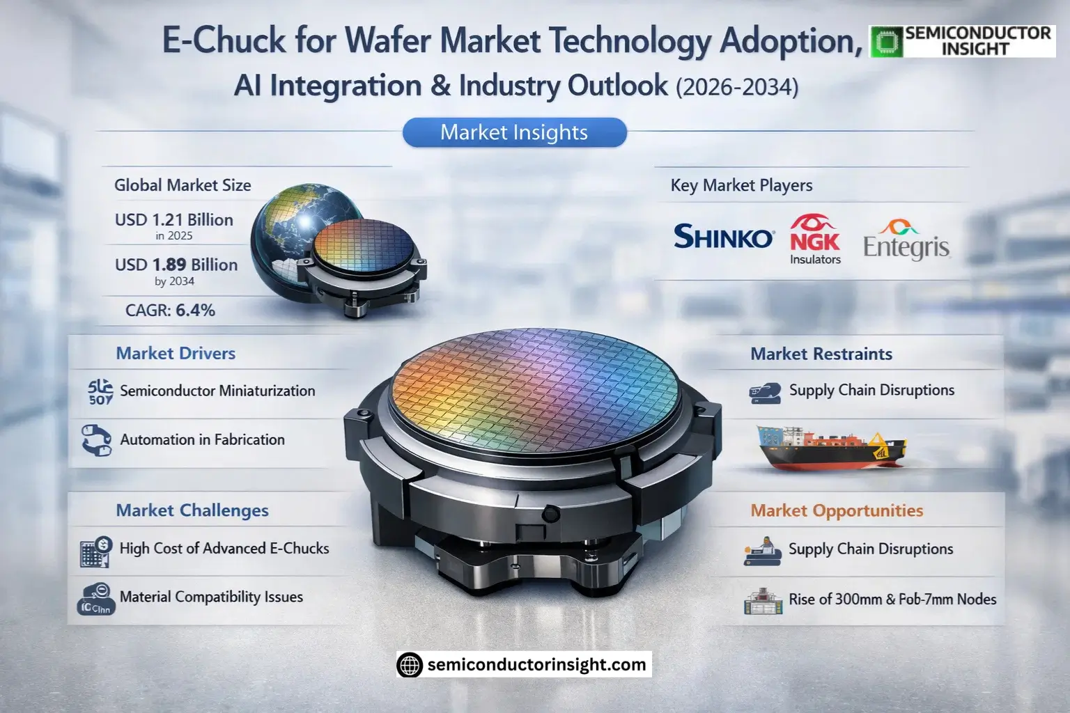
Global E-Chuck for Wafer Market size was valued at USD 1.21 billion in 2025. The market is projected to grow from USD 1.29 billion in 2026 to USD 1.89 billion by 2034, exhibiting a CAGR of 6.4% during the forecast period.
E-Chuck for Wafer are electrostatic clamping devices used in semiconductor manufacturing to securely hold silicon wafers during processes like etching, deposition, and ion implantation. These components utilize electrostatic force to maintain wafer stability without mechanical contact, ensuring precision while minimizing contamination risks.
The market growth is driven by increasing semiconductor fabrication investments and demand for advanced process nodes below 7nm, where wafer handling precision becomes critical. Key players such as SHINKO, NGK Insulators, and Entegris are expanding production capacities to meet rising demand from foundries like TSMC and Samsung.
MARKET DRIVERS
Growing Demand for Semiconductor Miniaturization
E-Chuck for Wafer Market is witnessing significant growth due to the increasing demand for smaller, more efficient semiconductor components. The rise of 5G technology, IoT devices, and advanced computing systems has accelerated the need for precise wafer handling solutions. E-Chucks play a crucial role in maintaining stability during semiconductor manufacturing, ensuring minimal contamination and high accuracy.
Automation in Semiconductor Fabrication
Automation trends in wafer processing are driving adoption of advanced E-Chuck systems. Manufacturers are investing in electrostatic chuck technology to enhance throughput and reduce manual intervention, leading to improved yield rates in high-volume production environments.
Additionally, the shift toward 300mm and larger wafers in foundries is creating demand for more sophisticated E-Chuck solutions capable of handling larger substrates with precision.
MARKET CHALLENGES
High Cost of Advanced E-Chuck Systems
The implementation of cutting-edge E-Chuck technology requires substantial capital investment, particularly for helium-cooled and multi-zone temperature control systems. This creates barriers to adoption for smaller semiconductor manufacturers operating with limited budgets.
Other Challenges
Technical Complexity in Material Compatibility
Developing E-Chucks that work seamlessly with new compound semiconductor materials (GaN, SiC) presents engineering challenges, requiring continuous R&D investments to maintain performance standards.
MARKET RESTRAINTS
Supply Chain Disruptions Impacting Semiconductor Equipment
Global supply chain challenges are affecting the timely delivery of critical components for E-Chuck manufacturing. Shortages of specialty ceramics and advanced thermal interface materials are causing production delays across the wafer equipment sector.
MARKET OPPORTUNITIES
Expansion of Advanced Packaging Applications
The growth of 3D IC packaging and heterogenous integration is creating new opportunities for specialized E-Chuck solutions. Manufacturers developing chucks capable of handling delicate interposers and thin wafers are gaining competitive advantage in this emerging segment.
E-Chuck for Wafer Market TrendsIncreasing Demand for Advanced Semiconductor Manufacturing
E-Chuck for Wafer Market is experiencing significant growth due to rising demand in semiconductor fabrication. As wafer sizes increase to 300mm and beyond, manufacturers require more precise electrostatic chucks to maintain positioning accuracy during processes like PVD, PECVD, and ion implantation. The transition to smaller process nodes below 7nm has further amplified the need for temperature uniformity and minimal particle contamination.
Other Trends
Material Innovations in E-Chuck Components
Leading manufacturers are investing in advanced ceramics like aluminum nitride and silicon carbide for improved thermal conductivity and durability. These materials enable better heat dissipation during high-power semiconductor processes while maintaining consistent electrostatic clamping force. Polyimide-based E-Chucks are gaining traction for lower-temperature applications due to their cost-effectiveness.
Regional Production Shifts and Supply Chain Optimization
Asia dominates E-Chuck for Wafer production with major suppliers establishing local manufacturing near semiconductor fabs in Taiwan, South Korea, and China. This geographic clustering reduces lead times and enables closer technical collaboration between equipment manufacturers and ESC suppliers. North American and European markets are seeing increased investments in domestic supply chains for strategic semiconductor components.
Competitive Landscape Developments
The market remains concentrated among specialized ceramic component manufacturers, with leaders like NGK Insulators and Kyocera expanding production capacity. Recent mergers between materials suppliers and equipment manufacturers aim to create vertically integrated solutions. Testing and validation capabilities are becoming key differentiators as process tolerances tighten in advanced nodes.
Technological Convergence in Wafer Handling Systems
Modern E-Chuck for Wafer designs increasingly incorporate integrated cooling channels, multi-zone temperature control, and real-time monitoring capabilities. This integration supports the semiconductor industry’s transition toward Industry 4.0 with smart equipment that can automatically adjust parameters for optimal process conditions.
COMPETITIVE LANDSCAPE
Key Industry Players
Leading players drive innovation in precision wafer handling technology
E-Chuck for Wafer Market is dominated by Japanese ceramic material specialists like NGK Insulators and Kyocera, which leverage their advanced ceramics expertise to command approximately 35% combined market share. SHINKO Electric Industries leads in high-precision bipolar electrode designs for 300mm wafer applications, with its products widely adopted by TSMC and Samsung for advanced node processing. The competitive landscape features vertical integration, with top players controlling critical material supply chains from alumina ceramics to polyimide films.
Niche specialists like Entegris and Creative Technology Corporation are gaining traction in specialized segments – particularly for etch and CVD applications requiring ultra-low contamination. Chinese manufacturers such as Beijing U-precision Tech are expanding rapidly with government-supported R&D investments, though still face challenges in high-end market validation. The market also sees emerging competition from semiconductor equipment OEMs developing in-house ESC solutions to secure supply chain resilience.
List of Key E-Chuck for Wafer Companies Profiled
- SHINKO
- NGK Insulators
- TOTO
- NTK CERATEC
- Entegris
- Sumitomo Osaka Cement
- LK ENGINEERING
- MiCo
- Kyocera
- Technetics
- Creative Technology Corporation
- Krosaki Harima Corporation
- TOMOEGAWA
- Beijing U-precision Tech
- AEGISCO
Segment Analysis:
| Segment Category | Sub-Segments | Key Insights |
| By Type |
|
Aluminum Nitride ESCs are emerging as preferred solutions due to superior thermal conductivity and electrical insulation properties:
|
| By Application |
|
300mm Wafer Processing dominates the market with several competitive advantages:
|
| By End User |
|
Foundries represent the largest demand segment with unique requirements:
|
| By Electrode Type |
|
Johnsen-Rahbek (JR) Type ESCs are gaining significant traction in the market:
|
| By Process Technology |
|
Etching Processes constitute the largest application area due to critical requirements:
|
Regional Analysis: E-Chuck for Wafer Market
Asia-Pacific
Tech Adoption Drivers
Localized R&D centers of major semiconductor equipment firms accelerate E-Chuck customization for regional wafer specifications. Japanese manufacturers pioneer AI-assisted alignment systems, while Chinese fabs prioritize cost-effective solutions for mid-range nodes.
AI Integration Trends
Smart E-Chuck systems with embedded IoT sensors are gaining traction across Korean mega-fabs. Predictive maintenance algorithms analyze wafer handling patterns to optimize E-Chuck performance between scheduled maintenance cycles.
Supply Chain Advantages
Regional clusters enable just-in-time E-Chuck component delivery. Local material science breakthroughs in electrostatic chuck ceramics reduce dependency on international suppliers for critical subsystems.
Future Outlook
Next-generation E-Chuck designs will emerge to support advanced packaging and chiplets. Market growth will concentrate in Southeast Asia as new semiconductor hubs develop in Malaysia and Singapore.
North America
The North American E-Chuck market benefits from strong R&D investments in semiconductor equipment. U.S. chipmakers focus on specialized E-Chuck solutions for compound semiconductor wafers used in defense and aerospace applications. Canadian research institutions collaborate with equipment manufacturers to develop novel chucking mechanisms. The region maintains technological leadership in E-Chuck control systems but faces challenges in scaling production volume compared to Asian counterparts. Nearshoring trends may create new opportunities for localized E-Chuck manufacturing clusters serving advanced packaging facilities.
Europe
European manufacturers emphasize E-Chuck solutions for specialized wafer types in automotive and industrial applications. Germany leads in precision mechanical components for wafer handling, while the Netherlands focuses on supporting EUV lithography requirements. Stringent environmental regulations drive development of energy-efficient E-Chuck systems. The region’s market remains smaller in volume but commands premium pricing for high-reliability solutions. Collaborative EU research programs aim to develop next-generation wafer handling technologies.
Middle East & Africa
Emerging semiconductor initiatives in the Middle East create new demand for E-Chuck systems, particularly in Israel’s thriving fabless ecosystem. UAE investments in semiconductor infrastructure may introduce new opportunities for wafer handling equipment. The region currently relies on imports but shows potential as a future growth market. Technical universities are establishing semiconductor engineering programs that include wafer handling system studies.
South America
Limited domestic semiconductor production restricts E-Chuck market size, though Brazil shows early-stage fab development. Most demand comes from research institutions and specialized electronics manufacturers. The region serves mainly as an endpoint in global supply chains, though local maintenance service providers are establishing expertise in E-Chuck refurbishment and repair.
Report Scope
This market research report provides a comprehensive analysis of the E-Chuck for Wafer Market, covering the forecast period 2025–2034. It offers detailed insights into market dynamics, technological advancements, competitive landscape, and key trends shaping the industry.
Key focus areas of the report include:
- Market Overview: The report begins with an overview outlining its current market scenario, key growth indicators, and industry transformation drivers. It discusses macroeconomic factors, demand–supply balance, regulatory landscape, and the strategic role of E-Chucks in semiconductor manufacturing equipment for applications such as PVD, PECVD, etching, and ion implantation.
- Market Size & Forecast: Historical data and future projections for revenue, unit shipments, and market value across major regions and segments.
- Segmentation Analysis: Detailed breakdown by product type (Alumina, Aluminum Nitride, Silicon Carbide, Polyimide), electrode type (Coulomb, Johnsen-Rahbek), structural form, and wafer size (200mm, 300mm).
- Regional Insights: Insights into market performance across North America, Europe, Asia-Pacific, Latin America, and the Middle East & Africa, including country-level analysis where relevant.
- Competitive Landscape: Profiles of leading market participants, including their product offerings, R&D focus, manufacturing capacity, pricing strategies, and recent developments such as mergers, acquisitions, and partnerships.
- Technology Trends & Innovation: Assessment of emerging technologies, material advancements, fabrication techniques, and evolving industry standards in electrostatic chuck manufacturing.
- Market Drivers & Restraints: Evaluation of factors driving market growth along with challenges, supply chain constraints, regulatory issues, and market-entry barriers.
- Stakeholder Insights: Insights for component suppliers, OEMs, system integrators, investors, and policymakers regarding the evolving ecosystem and strategic opportunities.
Primary and secondary research methods are employed, including interviews with industry experts, data from verified sources, and real-time market intelligence to ensure the accuracy and reliability of the insights presented.
FREQUENTLY ASKED QUESTIONS:
What is the current market size of E-Chuck for Wafer Market?
-> E-Chuck for Wafer Market size was valued at USD 1.21 billion in 2025. The market is projected to grow from USD 1.29 billion in 2026 to USD 1.89 billion by 2034, exhibiting a CAGR of 6.4% during the forecast period.
Which key companies operate in E-Chuck for Wafer Market?
-> Key players include SHINKO, NGK Insulators, TOTO, NTK CERATEC, Entegris, Sumitomo Osaka Cement, Kyocera, among others.
What are the key growth drivers?
-> Key growth drivers include increased semiconductor manufacturing investments, adoption of advanced process nodes, and rising demand for 300mm wafers.
Which region dominates the market?
-> Asia is the dominant market, with key semiconductor manufacturing hubs in China, Japan, and South Korea.
What are the emerging trends?
-> Emerging trends include material innovations (AlN, SiC), multi-electrode designs, and integrated thermal management solutions.
Get Sample Report PDF for Exclusive Insights
Report Sample Includes
- Table of Contents
- List of Tables & Figures
- Charts, Research Methodology, and more...