Market Insights
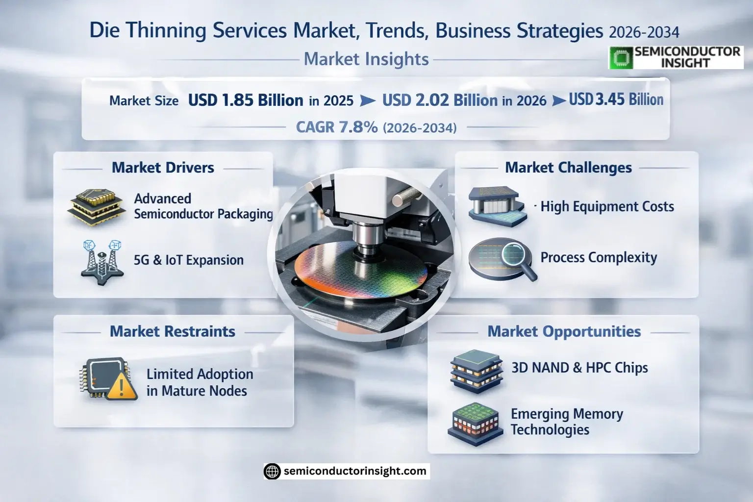
Global Die Thinning Services Market size was valued at USD 1.85 billion in 2025. The market is projected to grow from USD 2.02 billion in 2026 to USD 3.45 billion by 2034, exhibiting a CAGR of 7.8% during the forecast period.
Die thinning services involve precision wafer thinning processes such as grinding and etching, which are critical for semiconductor manufacturing. These services enhance device performance by reducing wafer thickness while maintaining structural integrity, enabling advanced packaging solutions like fan-out wafer-level packaging (FOWLP) and 3D IC integration.
The market growth is driven by increasing demand for compact and high-performance electronic devices, particularly in consumer electronics and automotive applications. Key players such as DISCO Corporation and Syagrus Systems are investing in advanced thinning technologies to cater to the rising need for miniaturization. Additionally, the expansion of AI and IoT applications further accelerates adoption, as thinner dies improve thermal management and power efficiency in next-generation chips.
MARKET DRIVERS
Growing Demand for Advanced Semiconductor Packaging
Die Thinning Services Market is experiencing significant growth due to the rising demand for advanced semiconductor packaging solutions. As devices become smaller and more powerful, manufacturers require ultra-thin dies to enable high-performance, compact designs. The shift toward 3D IC packaging and heterogeneous integration further accelerates adoption of precision die thinning services.
Expansion of 5G and IoT Applications
The proliferation of 5G networks and IoT devices has created substantial demand for thinner, energy-efficient semiconductor components. Die thinning services play a critical role in meeting the stringent performance and thermal management requirements of these applications. Mobile device manufacturers account for over 40% of the current demand for die thinning solutions.
Additionally, automotive semiconductor applications are driving new opportunities as electric vehicles require more advanced power electronics with thinner dies for improved heat dissipation.
MARKET CHALLENGES
High Equipment and Process Complexity
Die Thinning Services Market faces challenges from the high capital investment required for precision thinning equipment. Maintaining sub-micron accuracy while avoiding die damage during thinning remains a technical hurdle, especially for ultra-thin dies below 50μm.
Other Challenges
Yield Management and Cost Pressures
Achieving consistent yields at scale presents ongoing challenges, particularly with emerging materials like gallium nitride (GaN) and silicon carbide (SiC) which require specialized thinning processes.
MARKET RESTRAINTS
Limited Adoption in Mature Nodes
While die thinning services are essential for advanced packaging, their adoption remains limited in mature semiconductor nodes where cost sensitivity outweighs performance benefits. Many traditional applications continue to use standard thickness dies due to lower manufacturing costs.
MARKET OPPORTUNITIES
Emerging Memory and Logic Applications
Die Thinning Services Market is poised for growth through adoption in 3D NAND flash memory and high-performance computing chips. As memory stacking technologies advance, the need for precise thinning services will increase substantially. Leading foundries are already investing in dedicated die thinning capacity to support next-generation chips.
Die Thinning Services Market Trends
Increasing Demand for Advanced Semiconductor Packaging
Die Thinning Services Market is witnessing significant growth driven by the rising demand for advanced semiconductor packaging solutions. As consumer electronics and automotive industries require thinner, more efficient chips, wafer thinning technologies have become critical. Leading manufacturers are investing in precision grinding and etching techniques to meet these requirements.
Other Trends
Expansion of Grinding Technology Applications
Grinding remains the dominant technology in the Die Thinning Services market, accounting for the largest revenue share. Continuous improvements in grinding equipment and processes allow for thinner wafers with higher yields, particularly for high-performance computing and 5G applications.
Geographic Market Shifts
Asia-Pacific continues to lead in Die Thinning Services adoption, with China, Japan, and South Korea driving demand. North America and Europe maintain strong positions with specialized applications in aerospace and defense sectors. The market sees increasing competition from emerging players in Southeast Asia.
Industry Consolidation and Partnerships
The market is experiencing strategic partnerships between foundries and Die Thinning Service providers to ensure supply chain stability. Major players are acquiring smaller specialists to expand their technological capabilities and geographic reach in this competitive landscape.
Material Innovation Driving New Opportunities
Recent developments in compound semiconductor materials and new substrate technologies are creating additional demand for specialized Die Thinning Services. Manufacturers are adapting processes to handle diverse materials while maintaining precision and yield requirements for next-generation devices.
COMPETITIVE LANDSCAPE
Key Industry Players
Die Thinning Services Market Dominated by Specialized Semiconductor Players
Global Die Thinning Services Market is highly competitive, with specialized semiconductor equipment providers and wafer processing companies leading the segment. DISCO Corporation and Applied Materials currently dominate the market through their advanced grinding and etching technologies, collectively holding over 35% market share. The top five players, including Syagrus Systems and Optim Wafer Services, accounted for approximately 60% of 2025 revenues through their integrated solutions for advanced packaging applications in consumer electronics and automotive sectors.
Niche specialists like SIEGERT WAFER GmbH and NICHIWA KOGYO CO.,LTD. are gaining traction through regionally optimized solutions, particularly in Asian markets. Emerging players such as Aptek Industries and UniversityWafer, Inc. are focusing on R&D-intensive approaches, while foundry service providers like Phoenix Silicon International are expanding their die thinning capabilities to complement their existing semiconductor services. The market sees strong competition in precision thinning for 3D IC packaging and wafer-level packaging applications.
List of Key Die Thinning Services Companies Profiled
- DISCO Corporation
- Syagrus Systems
- Optim Wafer Services
- Silicon Valley Microelectronics, Inc.
- SIEGERT WAFER GmbH
- NICHIWA KOGYO CO.,LTD.
- Integra Technologies
- Valley Design
- AXUS TECHNOLOGY
- Helia Photonics
- Aptek Industries
- UniversityWafer, Inc.
- Micross
- Power Master Semiconductor Co., Ltd.
- Phoenix Silicon International
Segment Analysis:
| Segment Category | Sub-Segments | Key Insights |
| By Type |
|
Grinding dominates the Die Thinning Services Market due to:
|
| By Application |
|
Consumer Electronics remains the primary application driver because:
|
| By End User |
|
Foundries represent the most significant end-user segment as:
|
| By Wafer Size |
|
300mm wafers account for majority share due to:
|
| By Service Provider |
|
Pure-play Thinning Specialists maintain market leadership through:
|
Regional Analysis: Die Thinning Services Market
Asia-Pacific
Asia-Pacific maintains technology leadership with advanced temporary bonding/debonding systems and ultra-precision grinding equipment. Service providers consistently pioneer processes for thinner dies below 20μm while maintaining die strength for advanced packaging requirements.
Vertical integration with substrate manufacturers and test houses creates seamless workflow for customers. Many facilities co-locate thinning services with other back-end processes, reducing wafer handling risks and transportation costs for thin wafers.
Regional providers achieve 15-20% cost advantages through higher equipment utilization rates and shared engineering resources across multiple customer projects. Economies of scale allow competitive pricing for high-volume production orders.
ISO Class 1-3 cleanrooms are standard across leading facilities, with particulate controls meeting semiconductor-grade requirements. Comprehensive metrology capabilities ensure consistent thickness variation below ±2μm across 300mm wafers.
North America
The North American Die Thinning Services Market focuses on high-mix, low-to-medium volume specialized applications, particularly for aerospace, defense, and automotive sectors. Local providers emphasize flexible manufacturing capabilities to support diverse substrate materials and unconventional package sizes. Strong IP protection regimes attract innovative packaging developers requiring confidential die thinning process development. Regional advantages include proximity to major IDMs and fabless companies needing quick-turn prototyping services. The market sees increasing demand for compound semiconductor thinning services for GaN and SiC power devices.
Europe
Europe maintains specialized die thinning capabilities centered around automotive-grade reliability requirements. German and French providers lead in qualification processes for mission-critical applications. The region hosts several equipment manufacturers, enabling close collaboration between thinning service providers and machine developers for process optimization. Growing focus on heterogeneous integration for automotive radar and industrial IoT creates demand for advanced thinning services combined with wafer-level bonding techniques. Strict environmental regulations drive innovation in waste reduction and recycling of grinding slurries.
Middle East & Africa
Emerging investment in semiconductor packaging infrastructure creates niche opportunities for die thinning services in the region. Providers focus on serving local demand for consumer electronics while developing capabilities for MEMS and sensor applications. Government initiatives to develop technical expertise support workforce development in precision machining disciplines. Strategic location between European and Asian markets enables competitive logistics for certain customer segments requiring regional diversification of supply chains.
South America
The South American market remains in early development stages, with die thinning services primarily serving local electronics assembly needs. Brazil leads in establishing basic thinning capabilities for conventional packaging applications. Growing automotive manufacturing creates potential for expansion into more advanced thinning services. Limited local R&D infrastructure necessitates partnerships with international technology providers to upgrade capabilities for next-generation packaging requirements.
Report Scope
This market research report provides a comprehensive analysis of the Global Die Thinning Services Market, covering the forecast period 2025–2034. It offers detailed insights into market dynamics, technological advancements, competitive landscape, and key trends shaping the industry.
Key focus areas of the report include:
- Market Overview: The report begins with an overview outlining its current market scenario, key growth indicators, and industry transformation drivers. It discusses macroeconomic factors, demand–supply balance, regulatory landscape, and the strategic role of semiconductors in powering advancements across industries such as consumer electronics, automotive electronics, and data centers.
- Market Size & Forecast: Historical data and future projections for revenue, unit shipments, and market value across major regions and segments.
- Segmentation Analysis: Detailed breakdown by product type (Grinding, Etching, Others), application (Consumer Electronics, Automotive Electronics, Computer and Data Center), and end-user industry to identify high-growth segments.
- Regional Insights: Insights into market performance across North America, Europe, Asia, South America, and Middle East & Africa, including country-level analysis.
- Competitive Landscape: Profiles of leading market participants, including their product offerings, R&D focus, manufacturing capacity, and recent developments.
- Technology Trends & Innovation: Assessment of emerging technologies in wafer thinning and semiconductor fabrication techniques.
- Market Drivers & Restraints: Evaluation of factors driving market growth along with challenges in supply chain and regulatory environment.
- Stakeholder Insights: Strategic insights for semiconductor manufacturers, service providers, and investors.
Primary and secondary research methods are employed, including interviews with industry experts and data from verified sources to ensure accurate insights.
FREQUENTLY ASKED QUESTIONS:
What is the current market size of Die Thinning Services Market?
-> Die Thinning Services Market size was valued at USD 1.85 billion in 2025. The market is projected to grow from USD 2.02 billion in 2026 to USD 3.45 billion by 2034, exhibiting a CAGR of 7.8% during the forecast period.
Which key companies operate in Die Thinning Services Market?
-> Key players include Syagrus Systems, Optim Wafer Services, Silicon Valley Microelectronics, SIEGERT WAFER GmbH, NICHIWA KOGYO CO.,LTD., DISCO Corporation, and AXUS TECHNOLOGY, among others.
What are the key growth drivers?
-> Key growth drivers include increasing demand for thinner semiconductor devices, advancements in consumer electronics, and growth in automotive electronics applications.
Which region dominates the market?
-> Asia is the dominant market, with China estimated to reach USD million by 2034, while the U.S. market is valued at USD million in 2025.
What are the key product segments?
-> The market is segmented by type into Grinding (projected to reach USD million by 2034), Etching, and Others.
Get Sample Report PDF for Exclusive Insights
Report Sample Includes
- Table of Contents
- List of Tables & Figures
- Charts, Research Methodology, and more...


