
China AI Chip Substrate Market Insights
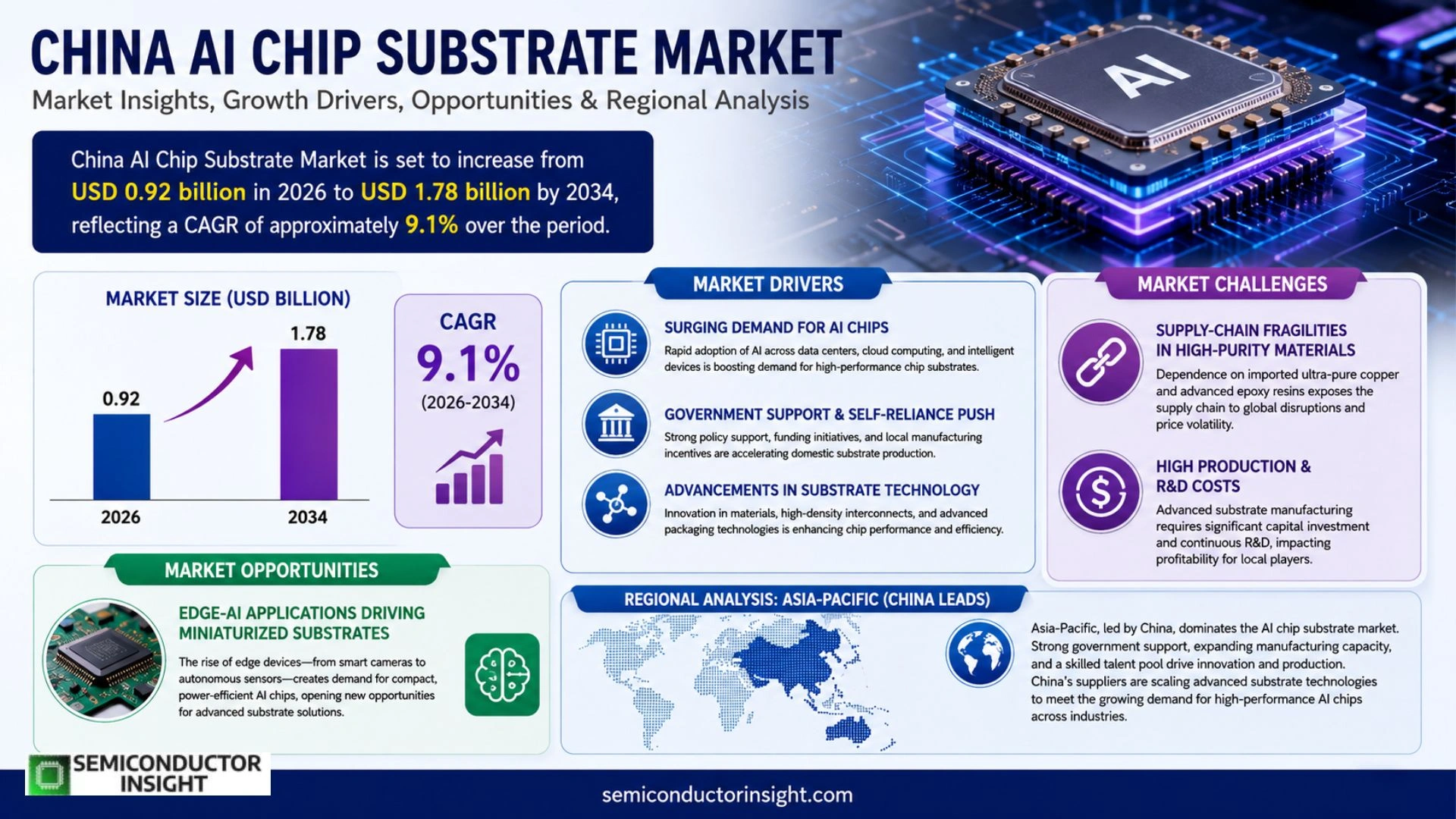
Global China AI Chip Substrate Market size was valued at USD 0.86 billion in 2025. The market is set to increase from USD 0.92 billion in 2026 to USD 1.78 billion by 2034, reflecting a CAGR of approximately 9.1 % over the period.
AI chip substrates are high‑performance interconnect layers that provide mechanical support and electrical routing for advanced processors used in artificial‑intelligence applications. These substrates incorporate materials such as copper‑clad laminates, glass‑fiber reinforced epoxy, and low‑dielectric‑constant polymers to enable dense signal transmission and thermal management.
The expansion is fueled by China’s aggressive AI strategy, rising demand for data‑center accelerators, and substantial public funding for semiconductor infrastructure. Moreover, advances in heterogeneous integration and the rollout of domestic fab capacities are encouraging adoption. Companies such as SMIC, Hua Hong Semiconductor, and JCET are actively expanding their substrate portfolios while collaborating with equipment suppliers.
MARKET DRIVERS
Rising Demand for Data‑Center AI Accelerators
Chinese hyperscale cloud operators are expanding their AI‑training capacity at a pace that outstrips traditional CPU growth. This forces OEMs to adopt high‑frequency substrates that can sustain the thermal and signal‑integrity requirements of modern AI chips. Manufacturers that can deliver substrates with tighter tolerances are likely to capture a larger share of these capital expenditures.
Targeted Government Incentives for Semiconductor Materials
The central and provincial authorities have rolled out subsidies aimed at the full stack of chip production, including the often‑overlooked substrate layer. By lowering effective material costs, these programmes make it feasible for midsize firms to invest in next‑generation copper‑core or organic‑laminate technologies. Companies that align their R&D roadmaps with policy priorities stand to benefit from both financial support and faster regulatory clearances.
➤ “Substrate performance is becoming the decisive factor for AI‑chip yield, especially as node sizes shrink below 5 nm,” notes a senior engineering director at a leading Chinese fab.
Beyond cost, the shift toward heterogeneous integration is reshaping design philosophies. Engineers are stitching memory, logic, and photonic elements onto a single substrate, which demands new dielectric formulations. Firms that master these multi‑layer stacks will unlock higher bandwidths and lower power envelopes, translating into a competitive edge in the AI workload market.
MARKET CHALLENGES
Supply‑Chain Fragilities in High‑Purity Materials
While domestic production of silicon wafers has grown, the ecosystem for ultra‑pure copper and advanced epoxy resins remains dependent on imported feedstock. Any disruption,whether geopolitical or logistical,can cascade into longer lead times for substrate orders. Customers may respond by increasing safety stock, which in turn elevates inventory costs across the supply chain.
Other Challenges
Talent Shortage
The substrate design discipline requires expertise in both materials science and high‑frequency signal engineering. Chinese universities are expanding curricula, yet the industry reports a gap of several thousand qualified engineers. Companies that invest early in training programs or strategic hiring from overseas will mitigate delays in product qualification.
Regulatory compliance adds another layer of complexity. New environmental standards for waste solvents and flame‑retardant additives are being enforced more rigorously, compelling manufacturers to redesign process flows. Failure to adapt promptly could result in production halts and potential penalties.
MARKET RESTRAINTS
Escalating Cost Structure of Advanced Materials
Transitioning from conventional FR‑4 to low‑loss, high‑frequency laminates introduces material premiums that can exceed 30 % of the bill of materials. When AI chip designers price their solutions aggressively to win market share, the added substrate cost squeezes profit margins for downstream assemblers. Enterprises that cannot pass these expenses onto end‑users may find pricing pressure eroding their viability.
Moreover, the capital intensity of upgrading production lines,such as installing precise laser drilling equipment or automated foil‑lamination units,requires multi‑year investment cycles. Smaller players lacking access to financing may be forced to exit the segment, leading to further concentration of market power among a few large incumbents.
MARKET OPPORTUNITIES
Edge‑AI Applications Driving Miniaturized Substrates
Edge devices,ranging from smart surveillance cameras to autonomous‑vehicle sensors,require compact AI chips that operate within strict power envelopes. This creates a niche for thin, lightweight substrates that incorporate embedded power‑distribution networks. Suppliers that can certify these substrates for automotive reliability standards will unlock a fast‑growing revenue stream.
In parallel, the emergence of heterogeneous integration platforms, where AI accelerators are co‑packaged with memory and analog front‑ends, opens a design space for multi‑die substrates. Companies that develop standardized interconnect architectures stand to become preferred partners for chipset vendors seeking quicker time‑to‑market. Such collaborations can accelerate overall ecosystem development and generate recurring engineering service income.
China AI Chip Substrate Market Trends
Accelerating Demand for AI‑Optimized Interconnects
China AI Chip Substrate Market is feeling the pressure of a swelling pipeline of AI workloads that require ever‑denser signal routing and tighter thermal budgets. Domestic data‑center operators are expanding accelerator farms faster than anticipated, compelling semiconductor fabs to source substrates that can sustain high‑frequency operation while minimizing power loss. This shift is not merely a reaction to headline AI projects; it reflects a broader strategic push to localise the entire AI hardware stack, reducing reliance on imported components. As a result, substrate manufacturers are prioritising process upgrades that deliver lower dielectric constants and enhanced copper adhesion, thereby enabling chip designs that push the envelope of compute density.
Other Trends
Material Innovation
Recent advances in low‑k polymer chemistry and glass‑fiber reinforced epoxy are reshaping the substrate landscape. Suppliers are blending these materials to achieve a balance between mechanical rigidity and signal integrity, a combination critical for next‑generation neural‑network processors. Concurrently, copper‑clad laminates are being engineered with finer line/space capabilities, allowing designers to route more interconnects within the same footprint. This material evolution is supported by joint R&D programmes between fabless AI chip designers and substrate producers, ensuring that the supply chain can keep pace with the rapid iteration cycles of AI algorithms.
Supply Chain Consolidation and Domestic Capability Build‑out
China’s semiconductor policy has encouraged a wave of investment in fab infrastructure, and substrate makers are consolidating to capture economies of scale. Companies such as SMIC, Hua Hong Semiconductor, and JCET have announced portfolio expansions that integrate substrate production into their wider manufacturing ecosystem. This vertical integration reduces lead times and improves coordination between wafer processing and substrate assembly, a critical advantage when dealing with the tight tolerances of AI chips. Moreover, the alignment of government funding with private capital has lowered barriers for smaller players to adopt advanced coating technologies, gradually widening the competitive field. For downstream AI system integrators, the resulting supply‑chain resilience translates into more predictable pricing and faster time‑to‑market for AI‑enabled products.
COMPETITIVE LANDSCAPE
Key Industry Players
China AI Chip Substrate Market Competitive Landscape
SMIC, Hua Hong Semiconductor and JCET dominate the substrate value chain, each leveraging extensive wafer‑fab capacity to offer integrated substrate solutions for AI accelerators. SMIC’s recent expansion of its 12‑inch line has allowed it to produce high‑density copper‑clad laminates that meet the thermal‑budget constraints of next‑generation AI cores. Hua Hong’s partnership with domestic equipment suppliers underlines a strategy of localized sourcing, reducing lead‑time and reinforcing supply‑chain resilience. JCET, while traditionally a packaging specialist, has broadened its portfolio to include low‑dielectric‑constant polymer layers, positioning itself as a one‑stop provider for heterogeneous integration projects. Collectively, these three firms command a sizable share of the market, setting pricing baselines and driving technology standards that ripple through downstream OEMs.
Beyond the frontrunners, a cadre of niche but technically sophisticated firms is shaping the market’s depth. Companies such as Unimicron China, Advanced Micro‑Fabrication (AMF), and Shanghai Xidian Microelectronics focus on specialty glass‑fiber reinforced epoxy substrates that cater to high‑frequency AI workloads. Fujian Jinhua and Hangzhou Silan contribute advanced thermal‑management laminates, addressing the heat‑dissipation challenges of densely packed AI chips. Emerging players like Sino IC and Nanjing Kongke have secured public‑funded projects to develop low‑κ polymer technologies, signaling a push toward cost‑effective yet high‑performance interconnects. The diversity of capabilities among these firms creates a competitive environment where material innovation, production scalability and strategic alliances become decisive factors for market share gains.
List of Key AI Chip Substrate Companies Profiled
- SMIC
- Hua Hong Semiconductor
- JCET Group
- Unimicron China
- Advanced Micro‑Fabrication (AMF)
- Shanghai Xidian Microelectronics
- Fujian Jinhua
- Hangzhou Silan
- Sino IC
- Nanjing Kongke
- ChipMOS Technologies
- ASE China
- Huaheng Precision
- Zhuhai Tianshan
- Guangdong Everbright
Segment Analysis:
| Segment Category | Sub-Segments | Key Insights |
| By Type |
|
Copper‑clad laminate dominates the type mix because it delivers the reliable high‑frequency signal integrity required by AI accelerator chips. – Provides excellent thermal conductivity that aligns with Chinese fab strategies for high‑density integration. – Established supply chains and mature processing heritage make it the preferred choice for both legacy and next‑generation designs. |
| By Application |
|
Data‑center accelerators emerge as the leading application segment due to strong governmental pushes for AI‑driven cloud services. – Substrates enable dense routing needed for large‑scale matrix multiplication cores. – Thermal management built into the substrate architecture supports the sustained high‑power operation of AI chips in server farms. |
| By End User |
|
Tech giants drive demand as they integrate AI chips into cloud platforms, AI‑as‑a‑service offerings, and intelligent software stacks. – Their scale enables close collaboration with substrate suppliers to co‑develop customized interconnect stacks. – Strategic emphasis on domestic supply security pushes them to prefer Chinese‑produced substrates that meet strict performance and reliability criteria. |
| By Integration Approach |
|
Heterogeneous integration is the most influential approach because it allows AI processors to combine memory, logic, and passive components on a single substrate. – Enables rapid time‑to‑market for AI accelerators tailored to specific workloads. – Aligns with China’s policy to boost vertical integration capabilities within its semiconductor ecosystem. |
| By Performance Tier |
|
High‑performance tier leads the market narrative as manufacturers target breakthroughs in deep‑learning throughput. – Substrate design focuses on ultra‑low loss signal paths and enhanced heat spreading. – The strategic push for sovereign AI compute capability reinforces investment in premium substrate solutions for flagship AI chips. |
Regional Analysis: China AI Chip Substrate Market
Asia‑Pacific
Companies are dissolving traditional silos between substrate fabrication and AI chip design. Collaborative roadmaps allow substrate engineers to anticipate power‑density trends, thereby tailoring dielectric compositions before silicon layout is frozen.
The region’s universities churn out specialists in materials science and nano‑fabrication, supplying a pipeline that fuels both start‑ups and incumbents, reinforcing the market’s inventive capacity.
Recent directives encourage joint ventures between substrate producers and AI chip founders, lowering entry barriers for niche players and accelerating technology diffusion across the value chain.
Growth in autonomous vehicles and smart manufacturing is prompting bespoke substrate solutions that can tolerate higher frequencies and stricter reliability standards.
North America
North American firms view China AI Chip Substrate Market as both a competitive benchmark and a sourcing opportunity. While most U.S. designers prefer domestic supply for security reasons, a subset is exploring dual‑sourcing strategies to tap the cost efficiencies of Asian substrates. This creates a nuanced dynamic where collaboration coexists with strategic hedging, compelling North American players to bolster their own substrate R&D to retain relevance.
Europe
European stakeholders are particularly attentive to sustainability criteria embedded within substrate manufacturing. The continent’s regulatory climate pushes suppliers toward greener chemistries, prompting European chipmakers to assess the environmental footprint of Asian‑sourced substrates. Consequently, joint sustainability projects are emerging, aiming to certify low‑impact production methods that satisfy EU standards while maintaining performance.
South America
In South America, market maturity remains embryonic, yet the region’s growing data‑center footprint has sparked interest in affordable AI chip substrates. Local assemblers are evaluating Chinese offerings as a gateway to cost‑effective AI deployment, balancing price advantages against concerns over long‑lead‑time logistics and intellectual‑property safeguards.
Middle East & Africa
The Middle East & Africa corridor is leveraging its expanding telecommunications infrastructure to trial AI‑enabled edge solutions. Reliance on imported substrates introduces a strategic imperative to develop regional capabilities, prompting governments to incentivize knowledge‑transfer initiatives with Chinese substrate firms.
Report Scope
This market research report provides a comprehensive analysis of the China AI Chip Substrate Market , covering the forecast period 2026–2034. It offers detailed insights into market dynamics, technological advancements, competitive landscape, and key trends shaping the industry.
Key focus areas of the report include:
- Market Overview: The report begins with an overview outlining its current market scenario, key growth indicators, and industry transformation drivers. It discusses macroeconomic factors, demand–supply balance, regulatory landscape, and the strategic role of semiconductors in powering advancements across industries such as automotive, telecommunications, consumer electronics, and industrial automation.
- Market Size & Forecast: Historical data and future projections for revenue, unit shipments, and market value across major regions and segments.
- Segmentation Analysis: Detailed breakdown by product type, technology, application, and end-user industry to identify high-growth segments and investment opportunities.
- Regional Insights: Insights into market performance across North America, Europe, Asia-Pacific, Latin America, and the Middle East & Africa, including country-level analysis where relevant.
- Competitive Landscape: Profiles of leading market participants, including their product offerings, R&D focus, manufacturing capacity, pricing strategies, and recent developments such as mergers, acquisitions, and partnerships.
- Technology Trends & Innovation: Assessment of emerging technologies, integration of AI/IoT, semiconductor design trends, fabrication techniques, and evolving industry standards.
- Market Drivers & Restraints: Evaluation of factors driving market growth along with challenges, supply chain constraints, regulatory issues, and market-entry barriers.
- Stakeholder Insights: Insights for component suppliers, OEMs, system integrators, investors, and policymakers regarding the evolving ecosystem and strategic opportunities.
Primary and secondary research methods are employed, including interviews with industry experts, data from verified sources, and real-time market intelligence to ensure the accuracy and reliability of the insights presented.
FREQUENTLY ASKED QUESTIONS:
What is the current market size of China AI Chip Substrate Market?
-> China AI Chip Substrate Market size is set to increase from USD 0.92 billion in 2026 to USD 1.78 billion by 2034, reflecting a CAGR of approximately 9.1 %
Which key companies operate in China AI Chip Substrate Market?
-> Key players include SMIC, Hua Hong Semiconductor, and JCET, among other domestic semiconductor manufacturers expanding their substrate portfolios.
What are the key growth drivers?
-> Key growth drivers include China’s aggressive AI strategy, rising demand for data‑center accelerators, substantial public funding for semiconductor infrastructure, and advances in heterogeneous integration.
Which region dominates the market?
-> China remains the dominant market, with Asia‑Pacific showing the fastest growth due to strong government support and expanding fab capacities.
What are the emerging trends?
-> Emerging trends include heterogeneous integration of AI chips, development of low‑dielectric‑constant polymer substrates, and increased adoption of advanced copper‑clad laminates for high‑performance interconnects.
Get Sample Report PDF for Exclusive Insights
Report Sample Includes
- Table of Contents
- List of Tables & Figures
- Charts, Research Methodology, and more...
 Download Sample Report PDF





