Key Statistics
Key Takeaways
- 12-inch BCD is the leading wafer-size segment because 300 mm manufacturing improves die-per-wafer economics and supports advanced BCD nodes with higher digital content, while 200 mm remains important for mature high-voltage and automotive power-management processes.
- Automotive electronics has the strongest application growth in the source market because electric vehicles, ADAS, infotainment, battery management and zonal electrical architectures require more PMIC, gate-driver and mixed-signal power functions per vehicle.
- Fabless semiconductor companies are the fastest-growing end-user group because specialized PMIC designers increasingly outsource manufacturing while concentrating capital on circuit architecture, firmware and customer-specific power solutions.
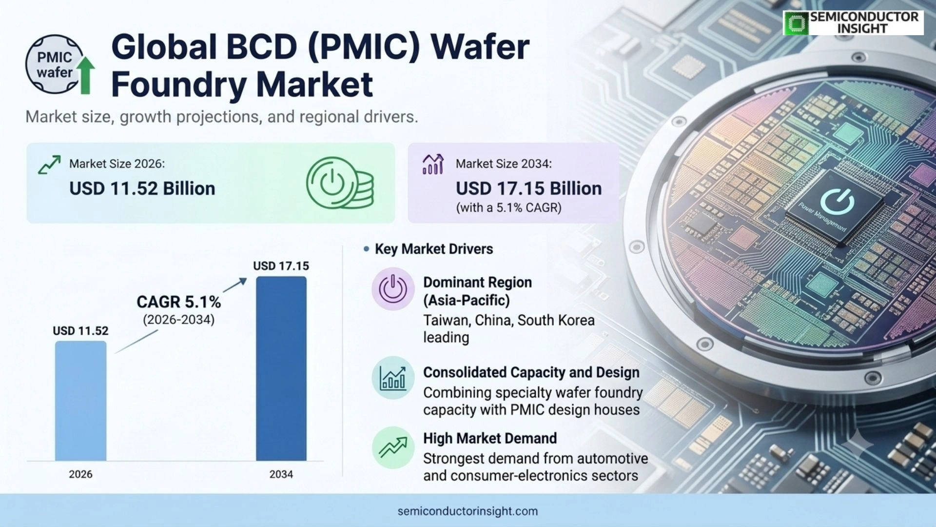
- Asia Pacific is the dominant region, with Taiwan at the center through TSMC, UMC, VIS and PSMC, while China is expanding domestic BCD capacity through SMIC, Hua Hong and other specialty foundries.
- BCD technology is moving to smaller nodes without abandoning mature platforms. TSMC now spans 0.6 µm to 22 nm BCD and UMC has launched a 55 nm BCD platform, while 90–180 nm processes remain attractive for high-voltage, automotive and industrial products.
BCD (PMIC) Wafer Foundry Market Overview
BCD (PMIC) Wafer Foundry market was valued at USD 10.96 billion in 2025 and is projected to reach USD 17.15 billion by 2034, representing a 5.1% CAGR during 2026–2034. The 2026 estimated market size is USD 11.52 billion. Asia Pacific is the dominant region because Taiwan, China, South Korea and other Asian markets combine specialty foundry capacity, PMIC design houses and large automotive and consumer-electronics demand.
BCD integrates bipolar devices, CMOS logic and DMOS power transistors on one wafer process so a single chip can combine control, analog precision and power handling. The architecture is well suited to PMICs, DC-DC converters, battery-management ICs, motor drivers, audio power and high-voltage interface products. Foundries compete by offering device libraries across several voltage classes, embedded non-volatile memory, thick metal, analog passives and automotive-qualified process flows.
Unlike leading-edge digital logic, BCD does not migrate uniformly to the smallest geometry. A 180 nm platform can remain economically superior for high-voltage devices and large analog components, while 90 nm, 65 nm, 55 nm and 40 nm BCD support more digital content, smaller die size and higher integration. The market therefore consists of overlapping generations rather than a simple replacement ladder, and customers select the node that gives the best total power, voltage, integration, cost and reliability.
AI infrastructure is creating a new high-current power-management opportunity alongside automotive and mobile demand. Server processors and accelerators require efficient conversion from 48 V or 12 V rails to low-voltage high-current domains near the load. TSMC has extended 0.18 µm Gen-2 BCD toward 100 V for 48 V server and EV systems, while Tower is using its 65 nm BCD platform for high-current point-of-load regulators targeting AI compute, cloud storage and telecom infrastructure.
Segment Analysis: By Type
By wafer size, the report segments the market into 12-inch BCD, 8-inch BCD and 6-inch BCD. 12-inch BCD leads because higher wafer productivity and newer process nodes improve economics for high-volume PMICs, while 8-inch capacity remains essential for mature automotive, industrial and high-voltage products where the process is already qualified and the die does not benefit enough from migration to justify a redesign.
| Wafer size / type | Manufacturing role | Market position |
|---|---|---|
| 12-inch BCD | 300 mm BCD supports advanced nodes such as 90 nm, 65 nm, 55 nm, 40 nm and future 22 nm platforms. Larger wafers provide more die per batch and pair well with higher automation, advanced lithography and dense digital integration. Foundries can use existing 300 mm infrastructure while tailoring high-voltage devices, thick metal and analog components for power-management applications. | Leading segment. The source report identifies 12-inch BCD as dominant because it offers better high-volume economics and supports complex automotive, mobile and AI power-management products. TSMC was an early production adopter of 12-inch BCD and Tower offers a 65 nm 300 mm power platform. |
| 8-inch BCD | 200 mm BCD remains widely used for 180 nm, 130 nm, 110 nm and other mature specialty processes. Equipment is fully depreciated in many fabs and the platform supports high-voltage LDMOS, analog devices, eNVM and automotive qualification. It is especially suitable where die size is driven by power devices rather than digital logic density. | A durable and capacity-sensitive segment. UMC, Tower, X-FAB, VIS and several Asian specialty foundries maintain strong 200 mm offerings. The economics can remain attractive for automotive and industrial products with long lifecycles and stable process qualifications. |
| 6-inch BCD | 150 mm lines serve legacy and specialty high-voltage products where volumes are lower and process migration offers limited economic benefit. Equipment and tooling costs can be low, but the smaller wafer size results in fewer die per batch and less automation than 200 mm or 300 mm manufacturing. | A declining but still relevant niche for mature specialty devices, regional foundries and products with long qualification histories. Migration occurs slowly because customers may prioritize continuity and proven reliability over lower cost per die. |
Technology node and integration-level segmentation
The report also segments demand by technology node and integration level. The 90 nm to 40 nm band is the most widely adopted because it balances logic density, analog performance and power-device capability. Nodes below 40 nm target highly integrated PMICs with substantial digital control, while 180 nm to 90 nm remains important for high voltage and automotive. System-on-chip BCD is gaining traction as designers integrate power stages, sensing, protection and control logic into fewer devices.
| Axis | Segments | Commercial implication |
|---|---|---|
| By Technology Node | 180nm–90nm · 90nm–40nm · Below 40nm | Mature nodes offer proven high-voltage devices and low mask cost, 90–40 nm provides a strong balance of digital density and analog/power performance, and sub-40 nm platforms target PMICs requiring much more embedded logic and smaller footprint. |
| By Integration Level | Discrete Power ICs · System-on-Chip Solutions · Power Management Modules | SoC BCD combines analog, logic and power functions on one die, reducing board area and interfaces. Discrete devices remain efficient for simple high-current functions, while modules combine several ICs and passives where system-level thermal or power density requires more integration. |
Segment Analysis: By Application
By application, the report covers Smart Phone, Automotive Electronics, Consumer Electronics and Industrial. Automotive shows the strongest growth because electrification and ADAS increase the number and power range of PMICs, gate drivers, motor controllers and battery-management functions. Smartphones remain a large volume market where smaller BCD nodes and high digital content help reduce die size and improve efficiency.
| Application | Demand characteristics |
|---|---|
| Automotive Electronics | The strongest growth application includes traction and auxiliary power, battery management, infotainment, ADAS, lighting, body electronics, motor drivers and zonal power distribution. Automotive BCD must meet stringent temperature, reliability and change-control requirements. Foundries compete on AEC-Q100-compatible flows, high-voltage LDMOS performance, embedded NVM and long product availability rather than only wafer price. |
| Smart Phone | Mobile devices use BCD PMICs for battery charging, application-processor power, display, audio, USB power delivery and RF-related power control. Advanced BCD nodes reduce die area and support more digital intelligence inside PMICs while maintaining efficient 5 V and other power devices. High annual volumes make die size and 300 mm cost economics especially important. |
| Consumer Electronics | PCs, wearables, home appliances, gaming systems and smart devices use a wide range of power-management and mixed-signal chips. Product lifecycles are shorter than automotive, so cost, integration and time to market carry more weight. BCD enables compact converters, audio amplifiers, LED drivers, chargers and battery-management functions across this diverse segment. |
| Industrial | Factory automation, robotics, HVAC, instrumentation, telecom and energy systems require motor drivers, gate drivers, power converters and high-voltage mixed-signal ICs. These products often use mature BCD nodes because they need rugged voltage capability, long lifecycle and stable analog behavior. Industrial customers value design kits, safe-operating-area data and reliable long-term wafer supply. |
Regional Analysis
Asia Pacific dominates the BCD (PMIC) Wafer Foundry market because Taiwan, China, South Korea and other Asian locations host many of the world’s leading specialty foundries and PMIC customers. Taiwan is the primary technology and capacity hub, while China is building domestic BCD capability. North America and Europe retain important design, automotive, industrial and specialty foundry positions through GlobalFoundries, Tower, X-FAB and regional customers.
How is BCD foundry capacity distributed across major semiconductor regions?
BCD capacity follows a different geography from leading-edge logic because mature 200 mm specialty fabs remain valuable alongside newer 300 mm lines. Taiwan combines both scales and has the broadest foundry ecosystem. China is expanding local power-management capacity, while North America and Europe emphasize automotive, industrial and data-center applications where process customization and long lifecycle support can justify premium specialty manufacturing.
| Region | Market position | Growth outlook | Demand profile | What decides supplier selection |
|---|---|---|---|---|
| Asia Pacific | Largest foundry base | High | Mobile, automotive & industrial | Process breadth, cost, capacity and automotive qualification |
| North America | Specialty and AI power hub | High | Server, automotive & industrial | High-current performance and local supply |
| Europe | Automotive/industrial specialty | Moderate to high | Automotive, industrial & energy | High-voltage capability and long lifecycle |
| South America | Small | Selective | Imported electronics & automotive | Foundry access through global fabless suppliers |
| Middle East & Africa | Niche / emerging | Selective | Specialty design and downstream demand | Technology access and global foundry partnerships |
Competitive Landscape
The report profiles TSMC, Samsung Foundry, GlobalFoundries, UMC, SMIC, Tower Semiconductor, PSMC, VIS, Hua Hong Semiconductor, HLMC, X-FAB, DB HiTek, Nexchip, Intel Foundry Services and GTA Semiconductor. TSMC and Samsung lead in advanced 300 mm BCD capability, while UMC, Tower, X-FAB and other specialty foundries compete through mature-node depth, automotive qualification and customized high-voltage device portfolios.
TSMC has one of the broadest BCD roadmaps, spanning mature high-voltage platforms through 22 nm development. Its 2025 technology updates include 55 nm BCD with new 5 V devices, second-generation 40 nm ultra-low-power BCD moving into volume production, 90 nm BCD in its second production year and extended 0.18 µm high-voltage options for AI servers and EVs. This breadth lets customers reuse a common foundry ecosystem across very different PMIC products.
UMC competes through a specialty-focused model and announced a 55 nm BCD platform in October 2025 with non-EPI, EPI and SOI variants. The offering supports multiple automotive grades and high voltage, while UMC’s wider BCD portfolio extends from mature geometries to 55 nm on 200 mm and 300 mm manufacturing. Process options and foundry design kits are important because power IC customers need device libraries that match specific voltage and isolation requirements.
Tower Semiconductor emphasizes high-value analog and power rather than scale leadership in digital logic. Its 65 nm 300 mm BCD platform and Gen3 LDMOS improvements target mobile, automotive and AI data-center power. X-FAB and other specialty foundries compete strongly where long lifecycle, high voltage, embedded NVM and automotive certification matter more than leading-edge geometry.
Competitive tier structure
| Tier | Companies | Basis of competition |
|---|---|---|
| Global 300 mm leaders | TSMC; Samsung Foundry; UMC | Advanced 55/40 nm and other 300 mm BCD, high volume, broad IP, automotive and mobile PMIC support |
| Specialty foundry leaders | Tower Semiconductor; X-FAB; GlobalFoundries; VIS; PSMC | Mature-node depth, high voltage, automotive reliability, analog customization and long product lifecycle |
| China / Asia challengers | SMIC; Hua Hong; HLMC; DB HiTek; Nexchip; GTA Semiconductor | Domestic PMIC ecosystem growth, 200 mm/300 mm expansion and cost-competitive regional capacity |
Key companies profiled in the report scope
- TSMC
- Samsung Foundry
- GlobalFoundries
- United Microelectronics Corporation (UMC)
- SMIC
- Tower Semiconductor
- PSMC
- VIS (Vanguard International Semiconductor)
- Hua Hong Semiconductor
- HLMC
- X-FAB
- DB HiTek
- Nexchip
- Intel Foundry Services (IFS)
- GTA Semiconductor Co., Ltd.
BCD Foundry Capacity & Manufacturing Analysis
BCD capacity is split between mature 200 mm specialty fabs and newer 300 mm lines. This mixed footprint is commercially important because customers do not always gain from shrinking a power-management design. Capacity planning therefore depends on voltage class, device area, digital content, automotive qualification and wafer-size economics. Foundries that can support both mature high-voltage processes and advanced high-integration platforms have a broader addressable market.
200 mm capacity remains tight in many specialty segments because the same fabs also serve display drivers, analog, MEMS, sensors and other mature products. Expanding an existing 200 mm line can be difficult because some tools are no longer produced in large volume. This supports migration of high-volume PMICs to 300 mm where process capability allows, but automotive customers may retain qualified 200 mm platforms for years to avoid redesign and reliability requalification.
300 mm BCD improves die-per-wafer economics and provides access to more advanced lithography, automation and process control. TSMC and Tower are examples of foundries using 300 mm for newer BCD nodes. However, the economic benefit depends on sustained utilization. A low-volume high-voltage product may still be better served on a mature 200 mm line with depreciated equipment and lower mask cost, so both wafer sizes will coexist through the forecast period.
Market Dynamics
Growth is supported by EVs, mobile power management, AI-server power delivery, industrial automation and the migration of high-content PMICs to advanced BCD nodes. Restraints include long automotive qualification, specialty-fab capacity constraints, node-migration cost and the complexity of integrating high-voltage devices with dense digital logic. Opportunities center on 300 mm BCD, 55/40 nm PMIC platforms, 48 V AI-server power and higher-voltage automotive integration.
MARKET DRIVERS
Drivers Impact Analysis*
| Factor | Forecast impact* | Geographic relevance | Impact timeline |
|---|---|---|---|
| Electric vehicles and ADAS | High | Asia Pacific, Europe, North America | Medium to long term |
| AI and data-center power delivery | High | North America, Asia Pacific | Medium to long term |
| Mobile / consumer PMIC integration | Medium to high | Asia Pacific | Persistent |
| Industrial automation and energy efficiency | Medium | Global | Persistent |
*Directional analytical rating; it is not a measured contribution to the headline CAGR.
Electric vehicles increase PMIC content
EVs add battery management, traction auxiliaries, charging, infotainment, ADAS, lighting and zonal power systems. These functions require efficient converters, drivers and monitoring circuits across a wide range of voltages. BCD is well suited because it combines analog precision, logic and power transistors on one die. Automotive qualification also creates long-lived foundry relationships once a process is approved.
AI servers create a new high-current BCD opportunity
AI racks distribute very large electrical power and require several conversion stages from facility or rack-level voltages down to sub-volt rails near processors. BCD platforms can integrate fast control logic with low-resistance LDMOS power devices, reducing losses and board area. TSMC’s 100 V 0.18 µm BCD extension and Tower’s 65 nm AI power work show this opportunity moving into foundry roadmaps.
Mobile devices reward higher digital integration
Smartphone PMICs increasingly include digital control, telemetry, charging intelligence and protection around power stages. Moving from 180/130 nm toward 90/55/40 nm BCD can reduce logic area and integrate more functions while maintaining required high-voltage devices. High smartphone volumes make die-size savings economically meaningful when the process is mature enough for strong yield.
Industrial systems sustain mature-node demand
Motor control, HVAC, robotics, factory equipment and energy systems need reliable power and analog functions but often do not require small digital geometry. Mature BCD nodes can deliver excellent voltage capability, low mask cost and proven reliability. This keeps 200 mm foundries economically relevant even as advanced BCD migrates to 300 mm.
MARKET RESTRAINTS
Restraints Impact Analysis*
| Factor | Forecast impact* | Geographic relevance | Impact timeline |
|---|---|---|---|
| Long automotive qualification cycles | High | Automotive supply chain | Persistent |
| Specialty 200 mm capacity constraints | Medium to high | Global | Short to medium term |
| Cost of node migration | Medium | Fabless PMIC designers | Persistent |
| High-voltage / digital integration complexity | High | Advanced BCD nodes | Persistent |
*Directional analytical rating; it is not a measured contribution to the headline CAGR.
Automotive process changes are slow
Automotive PMICs must meet reliability, traceability and quality requirements across temperature extremes and long vehicle lifetimes. Changing the foundry process can trigger device, package and system requalification, so customers often keep a mature node even when a newer one has lower die cost. This slows migration and makes market share sticky once a foundry has an approved platform.
Mature specialty capacity can be constrained
BCD shares 200 mm fabs with analog, display, sensor, MEMS and other specialty products. During strong demand, limited tool availability and long equipment lead times can restrict expansion. Customers may dual-source or migrate to 300 mm, but both actions require design and qualification work that cannot be completed instantly.
Shrinking the node does not always reduce total cost
High-voltage transistors, isolation structures and analog passives do not scale like digital logic. A smaller node may add mask layers and process complexity without reducing die area enough to justify the cost for a power-dominated design. PMIC companies must therefore evaluate the mix of logic and power content before migrating from 180 or 130 nm to advanced BCD.
Combining high voltage with dense logic is technically difficult
Advanced BCD must maintain low leakage, safe operating area and robust isolation while shrinking CMOS logic. These goals can conflict because high-voltage devices need larger structures and thicker oxides. Foundries invest heavily in device engineering and reliability characterization, raising development cost and limiting the number of suppliers able to support leading BCD platforms.
MARKET OPPORTUNITIES
Scale 55 nm and 40 nm BCD for high-content PMICs
New mobile, automotive and AI power products include more digital intelligence and telemetry. UMC’s 55 nm platform and TSMC’s 55/40 nm developments show growing foundry focus on this range. Suppliers that provide robust high-voltage options, embedded memory and automotive qualification can capture designs that would otherwise remain on 90/130 nm.
Address 48 V AI data-center power
Modern AI racks increasingly use 48 V distribution to reduce current and copper losses. Foundries can extend BCD voltage capability and optimize low-resistance LDMOS for intermediate-bus and point-of-load conversion. The opportunity extends from the power transistor itself to integrated controllers, drivers, telemetry and protection logic.
Use 300 mm migration to expand effective capacity
Moving suitable high-volume PMICs from 200 mm to 300 mm can increase die output per wafer and free mature lines for products that cannot migrate economically. The strategy is strongest for mobile and high-volume computing PMICs with enough digital content to benefit from smaller geometry and high 300 mm utilization.
Build specialized automotive BCD platforms
EV and ADAS applications need high voltage, temperature robustness, functional safety support and long lifecycle. Foundries can differentiate through automotive-qualified devices, embedded NVM, isolation options and documented reliability rather than trying to compete solely on node number. These platforms can create sticky multi-year design wins.
BCD (PMIC) Wafer Foundry Value Chain Analysis
Design requirements select the BCD node
A PMIC designer starts from system voltage, current, efficiency, control complexity and die-size targets. High-voltage and power-dominated products may fit mature nodes, while digitally intensive PMICs benefit from smaller geometry. The foundry’s PDK, device models and IP therefore influence architecture before the wafer process is selected, making design enablement a key part of foundry competition.
The BCD platform combines several device families
Foundries must integrate CMOS logic, bipolar devices, LDMOS, passive components, thick metal and sometimes embedded NVM in one process. Device interactions, isolation and reliability must remain controlled across a wide voltage range. This makes BCD more customized than commodity digital CMOS and creates switching costs once a customer’s design is qualified on a specific platform.
Wafer fabrication economics depend on product mix
200 mm fabs can be cost effective for mature, long-lived products, while 300 mm offers better die-per-wafer economics for high-volume advanced BCD. Yield, tool utilization and mask count determine the final wafer cost. Automotive customers add additional monitoring, traceability and screening requirements that increase manufacturing discipline but can support premium pricing.
Packaging converts wafer capability into system power density
PMIC packages must remove heat, carry high current and minimize parasitic resistance or inductance. Advanced packages, copper clips, exposed pads and multi-chip modules can increase power density beyond what the die alone provides. Foundry and package choices therefore interact, especially for AI server, automotive and fast-charging applications where electrical and thermal performance are tightly coupled.
Recent Developments in the BCD (PMIC) Wafer Foundry Market
Tower releases Gen3 BCD LDMOS technology for AI power
Tower Semiconductor announced a new generation of BCD power devices targeting the AI data-center power wall, advanced mobile PMICs and other high-current applications. The platform emphasizes improved LDMOS performance and demonstrates how AI-server power delivery is becoming a strategic specialty-foundry market.
Tower and Switch Semiconductor introduce AI-server regulator on 65 nm BCD
The companies announced a monolithic 12 V-to-1 V point-of-load regulator built on Tower’s 65 nm BCD platform. The device targets servers, AI compute, cloud storage and telecom and reaches up to 87% efficiency at a 20 A load.
UMC releases a new 55 nm BCD platform
UMC announced non-EPI, EPI and SOI 55 nm BCD options covering mobile, consumer, automotive and industrial power. The EPI solution supports operating voltage up to 150 V and targets demanding automotive reliability requirements.
TSMC expands 40 nm, 55 nm and high-voltage BCD roadmap
TSMC’s 2025 technology update states that second-generation 40 nm ultra-low-power BCD entered volume production, a new 55 nm 5 V device PDK was released and 0.18 µm Gen-2 BCD was extended toward 100 V for 48 V AI-server and EV power systems.
REPORT SCOPE & SEGMENTATION
| Attribute | Details |
|---|---|
| Study Period | 2019–2034 |
| Base Year | 2025 |
| Estimated Year | 2026 |
| Forecast Period | 2026–2034 |
| Historical Period | 2019–2025 |
| Market Size 2025 | USD 10.96 billion |
| Market Size 2034 | USD 17.15 billion |
| Growth Rate | CAGR of 5.1% from 2026–2034 |
| Unit | Value (USD Million/Billion) and wafer output where applicable |
| Segmentation | By Type, By Application, By End User, By Technology Node, By Integration Level, By Region |
| By Type | 12-inch BCD · 8-inch BCD · 6-inch BCD |
| By Application | Smart Phone · Automotive Electronics · Consumer Electronics · Industrial |
| By End User | IDMs · Fabless Semiconductor Companies · System Companies |
| By Technology Node | 180nm–90nm · 90nm–40nm · Below 40nm |
| By Integration Level | Discrete Power ICs · System-on-Chip Solutions · Power Management Modules |
| By Region | Each region analysed by wafer size, application, end user, technology node, integration level and country foundry ecosystemNorth AmericaUnited States, Canada, MexicoEuropeGermany, France, Austria, Belgium and other European marketsAsia PacificTaiwan, China, South Korea, Japan, Singapore and other Asian marketsSouth AmericaBrazil, Argentina and other South American marketsMiddle East & AfricaIsrael, Saudi Arabia, UAE, South Africa and other MEA markets |
| Key Companies Profiled | TSMC · Samsung Foundry · GlobalFoundries · United Microelectronics Corporation (UMC) · SMIC · Tower Semiconductor · PSMC · VIS (Vanguard International Semiconductor) · Hua Hong Semiconductor · HLMC · X-FAB · DB HiTek · Nexchip · Intel Foundry Services (IFS) · GTA Semiconductor Co., Ltd. |
| Customization Scope | Free report customization equivalent to up to four analyst working days with purchase. Addition or alteration to country, regional and segment scope. |
Frequently Asked Questions
What is the 2025 size of the BCD (PMIC) Wafer Foundry market?
The market was valued at USD 10.96 billion in 2025 and is projected to reach USD 17.15 billion by 2034. Those endpoint values imply a 5.1% CAGR during 2026–2034 and a normalized 2026 estimate of USD 11.52 billion. The endpoint-derived values are used consistently throughout this overview.
Which wafer size leads the market?
12-inch BCD is the leading type because 300 mm manufacturing provides better die-per-wafer economics for high-volume PMICs and supports advanced 90 nm, 65 nm, 55 nm and 40 nm platforms with higher digital content. Mature 8-inch BCD remains very important for automotive, industrial and high-voltage products.
Which application has the strongest growth?
Automotive electronics shows the strongest growth potential because electric vehicles, ADAS, battery management, infotainment, lighting and zonal power distribution require more PMICs and high-voltage mixed-signal devices per vehicle. Automotive qualification also creates long product lifecycles and durable foundry relationships.
Which region leads in 2025?
Asia Pacific is the dominant region, led by Taiwan’s broad specialty foundry ecosystem and expanding BCD capacity in China and South Korea. TSMC, UMC, VIS, PSMC, SMIC, Hua Hong, DB HiTek and other regional suppliers provide a wide range of mature and advanced BCD process platforms.
What is the estimated market size in 2026?
The normalized 2026 market size is USD 11.52 billion. It is calculated from the 2025 base of USD 10.96 billion and 2034 forecast of USD 17.15 billion using a constant annual growth factor, which produces a 5.1% CAGR for the 2026–2034 forecast period.
What technology node is most widely adopted?
The 90 nm to 40 nm range is the most widely adopted in the source segmentation because it offers a strong balance between digital logic density, analog performance, power-device capability and manufacturing cost. Mature 180–90 nm remains important for higher voltage, while sub-40 nm targets highly integrated PMICs.
Why does 8-inch BCD remain important?
Many automotive and industrial power devices are already qualified on 180 nm, 130 nm or similar 200 mm platforms. High-voltage transistors and analog passives do not scale like digital logic, so migration to a smaller node may not reduce total cost enough to justify redesign and requalification. Mature capacity therefore remains economically durable.
How is AI changing BCD foundry demand?
AI servers create demand for efficient high-current conversion close to processors and accelerators. Foundries are extending BCD toward lower-resistance power devices, advanced digital control and higher voltage ranges for 48 V rack architectures. Tower and TSMC have both highlighted AI-server power in recent BCD technology developments.
What are the main market restraints?
The main restraints are long automotive qualification cycles, constrained specialty 200 mm capacity, the cost of migrating mature designs to smaller nodes and the technical difficulty of integrating high-voltage devices with dense digital logic. These factors slow technology transitions and keep several BCD generations in production simultaneously.
What does the report cover?
The report covers 12-inch, 8-inch and 6-inch BCD; smartphone, automotive, consumer and industrial applications; IDM, fabless and system-company end users; 180 nm through sub-40 nm node bands; discrete, SoC and power-module integration; five global regions; capacity analysis; and all profiled foundries.
Research Sources & Evidence Base
View primary and authoritative evidence used in this overview
- TSMC. Bipolar-CMOS-DMOS Technology – Official foundry description covering 0.6 µm to 22 nm BCD, 55 nm and 40 nm platforms, 90 nm volume production and high-voltage extensions.
- UMC. BCD Technology Platform – Official UMC description of BCD from mature nodes through 55 nm, 200/300 mm manufacturing, voltage ranges and embedded-memory options.
- UMC. UMC releases 55 nm BCD platform – October 2025 official announcement covering non-EPI, EPI and SOI options for mobile, automotive and industrial power.
- Tower Semiconductor. Gen3 BCD technology addressing AI power – March 2026 official announcement on high-current LDMOS and AI data-center power-management applications.
- Tower Semiconductor. 65 nm BCD AI and server power collaboration – November 2025 official evidence on a 12 V-to-1 V regulator targeting AI compute and cloud infrastructure.
- TSMC. 2025 Annual Report – Primary source for 2025 BCD technology progress, volume production and power-management roadmap.

Get Sample Report PDF for Exclusive Insights
Report Sample Includes
- Table of Contents
- List of Tables & Figures
- Charts, Research Methodology, and more...
 Download Sample Report PDF