MARKET INSIGHTS
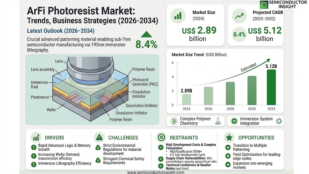
The global ArFi Photoresist Market size was valued at US$ 2.89 billion in 2024 and is projected to reach US$ 5.12 billion by 2032, at a CAGR of 8.4% during the forecast period 2025-2032.
ArFi photoresists are light-sensitive materials used in semiconductor manufacturing for advanced lithography processes at the 193nm wavelength with immersion techniques. These specialized chemical formulations enable the fabrication of integrated circuits with finer feature sizes, making them critical for cutting-edge chip production. Key product variants include formulations optimized for 8-inch and 12-inch wafers, with differing chemical compositions tailored for specific semiconductor applications.
The market growth is primarily driven by increasing demand for advanced semiconductor devices, particularly in artificial intelligence and 5G applications. However, supply chain challenges and the complexity of developing next-generation photoresists pose hurdles for manufacturers. Leading players such as Shin-Etsu Chemical and JSR Corporation continue to invest heavily in R&D to maintain technological leadership in this highly specialized market segment.
 MARKET DYNAMICS
MARKET DRIVERS
Expansion of Semiconductor Fabrication Capabilities to Accelerate Market Growth
The global ArFi photoresist market is experiencing significant growth driven by expanding semiconductor fabrication capabilities worldwide. As chipmakers transition to more advanced process nodes below 10nm, demand for ArFi (Argon Fluoride Immersion) lithography solutions has surged. Major foundries are aggressively investing in new fabrication facilities, with over 40 new semiconductor plants announced globally since 2021. This manufacturing expansion directly correlates with increased consumption of high-performance photoresists capable of supporting finer feature patterning. The transition toward 3D NAND flash memory and advanced DRAM technologies particularly benefits the ArFi photoresist segment, as these applications require the precision offered by 193nm immersion lithography.
Technological Advancements in Photoresist Formulations to Drive Adoption
Continuous innovation in chemically amplified resist (CAR) formulations presents a crucial driver for the ArFi photoresist market. Recent developments have focused on improving resolution, line edge roughness, and sensitivity characteristics – the critical triumvirate of photoresist performance. Advanced resist platforms now enable fabrication of features below 30nm with improved process windows and defect control. The introduction of metal-oxide resists has been particularly impactful, offering superior etch resistance and pattern fidelity compared to traditional polymer-based materials. Furthermore, the integration of machine learning in photoresist development has accelerated formulation optimization, reducing time-to-market for next-generation materials.
Growing Demand for Advanced Packaging Solutions to Fuel Market Expansion
The proliferation of advanced packaging technologies represents another significant growth driver for ArFi photoresist products. As the electronics industry embraces heterogeneous integration approaches like 2.5D/3D IC packaging, fan-out wafer-level packaging (FOWLP), and chiplet architectures, demand for precision lithography materials has intensified. These packaging methods require photoresists capable of accommodating high aspect ratio features and multi-layer patterning with stringent overlay requirements. The advanced packaging market segment is projected to grow at approximately 8% CAGR through 2030, creating sustained demand for specialized ArFi photoresist solutions tailored for packaging applications.
MARKET RESTRAINTS
High Development Costs and Complex Formulation Challenges to Limit Market Penetration
The ArFi photoresist market faces significant restraints due to the substantial R&D investments and technical barriers associated with advanced resist development. Creating photoresist materials that meet the stringent requirements of leading-edge semiconductor nodes requires extensive expertise in polymer chemistry, photochemistry, and materials science. The development cycle for new resist platforms typically spans 3-5 years with costs often exceeding $50 million for comprehensive qualification. This high barrier to entry limits participation to only a handful of well-capitalized chemical suppliers with established semiconductor materials portfolios.
Other Restraints
Supply Chain Vulnerabilities
The concentrated nature of photoresist supply chains presents operational risks, particularly given geopolitical tensions in key semiconductor manufacturing regions. Nearly 80% of advanced photoresist production capacity resides in just a few countries, creating potential bottlenecks during periods of trade friction or logistical disruptions. These vulnerabilities could restrict market growth if alternative supply sources aren’t developed.
Technical Limitations at Smaller Nodes
As semiconductor manufacturing progresses toward sub-5nm nodes, the inherent resolution limitations of 193nm lithography become increasingly apparent. While multiple patterning techniques have extended ArFi’s usefulness, the added process complexity drives up costs and reduces yields. This creates economic pressure for chipmakers to transition to alternative lithography methods, potentially capping long-term growth for traditional ArFi photoresist products.
MARKET CHALLENGES
Stringent Environmental Regulations to Challenge Material Development
The photoresist industry faces growing regulatory scrutiny regarding chemical safety and environmental impact, presenting significant challenges for market participants. New regulatory frameworks are mandating reductions in volatile organic compound (VOC) emissions and restricting certain solvent systems traditionally used in resist formulations. Compliance with evolving regulations like REACH and TSCA requires costly reformulation efforts and environmental impact assessments. These regulatory pressures coincide with heightened industry focus on sustainability, forcing manufacturers to balance performance requirements with environmental considerations.
Other Challenges
Technical Barriers in Extreme Ultraviolet (EUV) Transition
The semiconductor industry’s gradual shift toward EUV lithography creates competitive pressures for ArFi photoresist suppliers. While EUV adoption remains limited by throughput and cost considerations, its superior resolution capabilities pose a long-term threat to 193nm immersion lithography. Photoresist manufacturers must strategically allocate resources between maintaining traditional product lines while developing EUV-compatible materials.
Material Purity Requirements
Achieving the necessary purity levels for advanced photoresists presents ongoing technical challenges. Modern semiconductor fabs demand resist materials with metal contamination levels below parts-per-billion thresholds. Maintaining these purity standards through complex synthesis and purification processes significantly increases manufacturing costs and complexity.
MARKET OPPORTUNITIES
Emerging Applications in Advanced Memory and Logic Devices to Create New Growth Avenues
The ArFi photoresist market stands to benefit from expanding applications in next-generation memory and logic devices. Emerging non-volatile memory technologies like MRAM and ReRAM require specialized lithography materials capable of patterning complex multilayer structures. Similarly, the development of gate-all-around (GAA) transistor architectures in leading-edge logic devices demands photoresists with enhanced profile control capabilities. These technological transitions create opportunities for material suppliers to develop application-specific resist formulations catering to unique processing requirements.
Geographic Expansion in Semiconductor Manufacturing to Drive Regional Growth
Government initiatives to establish domestic semiconductor ecosystems in previously underserved regions present compelling growth opportunities for photoresist suppliers. Major markets including the European Union, India, and Southeast Asia are implementing substantial incentive programs to attract semiconductor manufacturing investment. As new fabrication facilities come online in these regions, demand for localized photoresist supply chains will intensify, encouraging material suppliers to expand distribution networks and technical support capabilities in emerging semiconductor hubs.
Development of Hybrid Lithography Approaches to Sustain Market Relevance
The growing adoption of hybrid lithography strategies combining ArFi with EUV and multi-patterning techniques offers opportunities to extend the technology’s commercial viability. As foundries implement cost-sensitive mixed-mode lithography solutions, demand arises for photoresist products specifically optimized for these hybrid processes. Material suppliers that can develop resists facilitating seamless integration between different lithography approaches will maintain competitive advantages during the semiconductor industry’s transitional period toward EUV dominance.
ARFI PHOTORESIST MARKET TRENDS
Increasing Semiconductor Miniaturization Driving Demand for ArFi Photoresists
The global ArFi (Argon Fluoride Immersion) photoresist market is experiencing significant growth due to the rising demand for advanced semiconductor manufacturing processes. With semiconductor nodes shrinking below 10nm, ArFi photoresists have become critical in lithography applications, providing superior resolution and pattern fidelity compared to traditional KrF and ArF photoresists. The market is projected to grow at a compound annual growth rate (CAGR) of approximately 7.5% from 2024 to 2032, as manufacturers increasingly adopt extreme ultraviolet (EUV)-compatible and high-performance photoresists. The ability of ArFi photoresists to enable finer feature patterning in memory and logic chips positions them as essential materials for next-generation chip production.
Other Trends
Expansion in Advanced Packaging Applications
The growing adoption of 2.5D and 3D IC packaging is fueling demand for ArFi photoresists, as these materials play a crucial role in through-silicon via (TSV) and redistribution layer (RDL) patterning. Advanced packaging technologies are increasingly used in high-performance computing (HPC), artificial intelligence (AI) chips, and 5G applications, where precision is paramount. The market for ArFi photoresists in advanced packaging is expected to surpass $850 million by 2030, driven by innovations in wafer-level packaging (WLP) and heterogeneous integration. Furthermore, the transition towards fan-out wafer-level packaging (FOWLP) is creating additional opportunities as chipmakers seek thinner and more efficient interconnect solutions.
Shift Towards Larger Wafer Sizes in Semiconductor Manufacturing
The semiconductor industry’s shift from 8-inch to 12-inch wafers is reshaping the ArFi photoresist market, with 12-inch wafer production accounting for over 60% of global capacity. Foundries and integrated device manufacturers (IDMs) are increasingly investing in 12-inch wafer fabs to achieve cost efficiencies and higher yields, directly boosting the demand for high-volume-compatible ArFi photoresists. While 8-inch wafer manufacturing remains crucial for specialized applications such as power devices and MEMS, the 12-inch segment is projected to grow at a CAGR of nearly 8% through 2032. Additionally, supply chain resilience concerns are prompting regional expansion of semiconductor fabs, particularly in the U.S. and Europe, further driving photoresist consumption.
COMPETITIVE LANDSCAPE
Key Industry Players
Market Leaders Invest in R&D and Strategic Expansions to Capture Larger Shares
The global ArFi photoresist market demonstrates a moderately consolidated competitive landscape, dominated by established chemical and semiconductor material manufacturers. Sumitomo Chemical Co., Ltd. and Shin-Etsu Chemical Co., Ltd. jointly command nearly 35% of the market share as of 2024, leveraging their decades of experience in high-performance photoresist formulations and strong distribution networks across Asia and North America.
DuPont maintains a robust position through its advanced ArFi photoresist solutions tailored for cutting-edge semiconductor nodes, particularly in the 12-inch wafer segment. Meanwhile, Fujifilm Corporation has been aggressively expanding its market presence through technological collaborations with leading foundries, securing approximately 15% of global revenue share.
Mid-sized players like TOKYO OHKA KOGYO CO., LTD. are gaining traction by focusing on niche applications such as advanced packaging and MEMS devices. Their specialized formulations cater to emerging demands in IoT and automotive semiconductor sectors, driving above-market growth rates.
The competitive intensity continues to rise as LG Chem and Mitsui Chemicals Inc. allocate substantial R&D budgets toward next-generation ArFi photoresists with improved resolution and etch resistance. These developments aim to address the industry’s shift toward sub-7nm process nodes and 3D NAND memory production.
List of Key ArFi Photoresist Manufacturers
- Sumitomo Chemical Co., Ltd. (Japan)
- DuPont (U.S.)
- Shin-Etsu Chemical Co., Ltd. (Japan)
- Fujifilm Corporation (Japan)
- LG Chem (South Korea)
- Mitsui Chemicals Inc. (Japan)
- Everlight Chemical Industrial Co. (Taiwan)
- TOKYO OHKA KOGYO CO., LTD. (Japan)
Segment Analysis:
By Type
8 Inch Wafer Segment Leads the Market Due to High Adoption in Foundry Applications
The market is segmented based on type into:
- 8 Inch Wafer
- 12 Inch Wafer
- Others
By Application
Advanced Packaging Segment Dominates Owing to Rising Semiconductor Miniaturization Trends
The market is segmented based on application into:
- Advanced Packaging
- MEMS Devices
- LED Devices
- Others
By Technology Node
Sub-20nm Technology Node Segment Grows Rapidly for High-Performance Computing Applications
The market is segmented based on technology node into:
- Above 180nm
- 90nm-180nm
- 45nm-90nm
- 20nm-45nm
- Sub-20nm
By End User
Foundries Maintain Market Leadership Through High-Volume Semiconductor Production
The market is segmented based on end user into:
- Foundries
- IDMs
- OSATs
- Research Institutes
Regional Analysis: ArFi Photoresist Market
North America
The North American ArFi photoresist market is primarily driven by robust semiconductor demand from the U.S., where leading manufacturers are investing heavily in advanced chip fabrication technologies. With the CHIPS Act allocating $52 billion to boost domestic semiconductor production, local demand for high-precision ArFi photoresists is accelerating. These materials are critical for manufacturing sub-20nm node chips used in AI, 5G, and automotive applications. While environmental regulations on solvent-based resists remain strict, suppliers are adapting with EUV-compatible formulations to meet evolving industry needs. Key players like DuPont maintain strong R&D footprints in the region, positioning North America as an innovation hub.
Europe
Europe’s market growth is tempered by limited local semiconductor production capacity compared to Asia, but strategic initiatives like the European Chips Act aim to double the region’s market share to 20% by 2030. Germany and France are leading adopters of ArFi technology for specialized applications in automotive and industrial IoT chips. Manufacturers face pressure to comply with stringent EU chemical regulations, prompting a shift toward more sustainable photoresist chemistries. Collaborative R&D between academic institutions and chemical companies, particularly in photoresist purification processes, is helping bridge the technology gap with Asian competitors while maintaining high purity standards.
Asia-Pacific
Dominating over 65% of global ArFi photoresist consumption, Asia-Pacific is the undisputed market leader due to concentrated semiconductor manufacturing in Taiwan, South Korea, and China. Leading-edge fabs like TSMC and Samsung drive relentless demand for high-performance formulations compatible with immersion lithography. However, the market faces supply chain vulnerabilities, as seen during recent material shortages that exposed regional over-reliance on Japanese suppliers. Local production is expanding, with Chinese manufacturers making significant inroads in mid-range photoresist segments. While cost competition is intense, quality improvements are enabling Asian producers to gradually challenge established players in high-end applications.
South America
The South American market remains in nascent stages, with Brazil showing the most potential as it develops basic semiconductor packaging capabilities. Most ArFi photoresist demand stems from multinational companies with local assembly operations rather than cutting-edge fabrication. Limited domestic expertise in advanced lithography and reliance on imports constrain market growth, although educational partnerships with foreign universities aim to build technical capabilities. Economic instability and currency fluctuations further discourage major investments in photoresist production facilities, keeping the region dependent on global suppliers.
Middle East & Africa
This emerging region is currently focused on establishing foundational semiconductor ecosystems, with the UAE and Israel making targeted investments in specialized chip design rather than fabrication. While direct ArFi photoresist consumption is minimal, growing interest in compound semiconductors for defense and aerospace applications could create niche demand. Regional governments are actively courting semiconductor equipment vendors, which may gradually stimulate supporting material markets. However, absent major fabrication projects, photoresist adoption will likely remain confined to research institutions and small-scale prototyping facilities in the medium term.
Report Scope
This market research report provides a comprehensive analysis of the global and regional ArFi Photoresist markets, covering the forecast period 2025–2032. It offers detailed insights into market dynamics, technological advancements, competitive landscape, and key trends shaping the industry.
Key focus areas of the report include:
- Market Size & Forecast: Historical data and future projections for revenue, unit shipments, and market value across major regions and segments.
- Segmentation Analysis: Detailed breakdown by product type, wafer size, application, and end-user industry to identify high-growth segments and investment opportunities.
- Regional Outlook: Insights into market performance across North America, Europe, Asia-Pacific, Latin America, and the Middle East & Africa, including country-level analysis where relevant.
- Competitive Landscape: Profiles of leading market participants, including their product offerings, R&D focus, manufacturing capacity, pricing strategies, and recent developments such as mergers, acquisitions, and partnerships.
- Technology Trends & Innovation: Assessment of emerging photolithography technologies, semiconductor fabrication techniques, and evolving industry standards for advanced node semiconductor manufacturing.
- Market Drivers & Restraints: Evaluation of factors driving market growth along with challenges, supply chain constraints, regulatory issues, and market-entry barriers.
- Stakeholder Analysis: Insights for chemical suppliers, semiconductor manufacturers, foundries, investors, and policymakers regarding the evolving ecosystem and strategic opportunities.
Primary and secondary research methods are employed, including interviews with industry experts, data from verified sources, and real-time market intelligence to ensure the accuracy and reliability of the insights presented.
FREQUENTLY ASKED QUESTIONS:
What is the current market size of Global ArFi Photoresist Market?
-> ArFi Photoresist Market size was valued at US$ 2.89 billion in 2024 and is projected to reach US$ 5.12 billion by 2032, at a CAGR of 8.4% during the forecast period 2025-2032.
Which key companies operate in Global ArFi Photoresist Market?
-> Key players include Sumitomo Chemical Co., Ltd., DuPont, Shin-Etsu Chemical Co., Ltd., Fujifilm Corporation, LG Chem, Mitsui Chemicals Inc., Everlight Chemical Industrial Co., and TOKYO OHKA KOGYO CO., LTD.
What are the key growth drivers?
-> Key growth drivers include increasing demand for advanced semiconductor devices, expansion of foundry capacities, and technological advancements in photolithography processes.
Which region dominates the market?
-> Asia-Pacific dominates the market, accounting for over 65% of global demand, driven by semiconductor manufacturing hubs in Taiwan, South Korea, and China.
What are the emerging trends?
-> Emerging trends include development of EUV-compatible photoresists, adoption of new resist chemistries for sub-10nm nodes, and increasing R&D investments in advanced materials.

Get Sample Report PDF for Exclusive Insights
Report Sample Includes
- Table of Contents
- List of Tables & Figures
- Charts, Research Methodology, and more...