Any-layer HDI PCB Market Insights
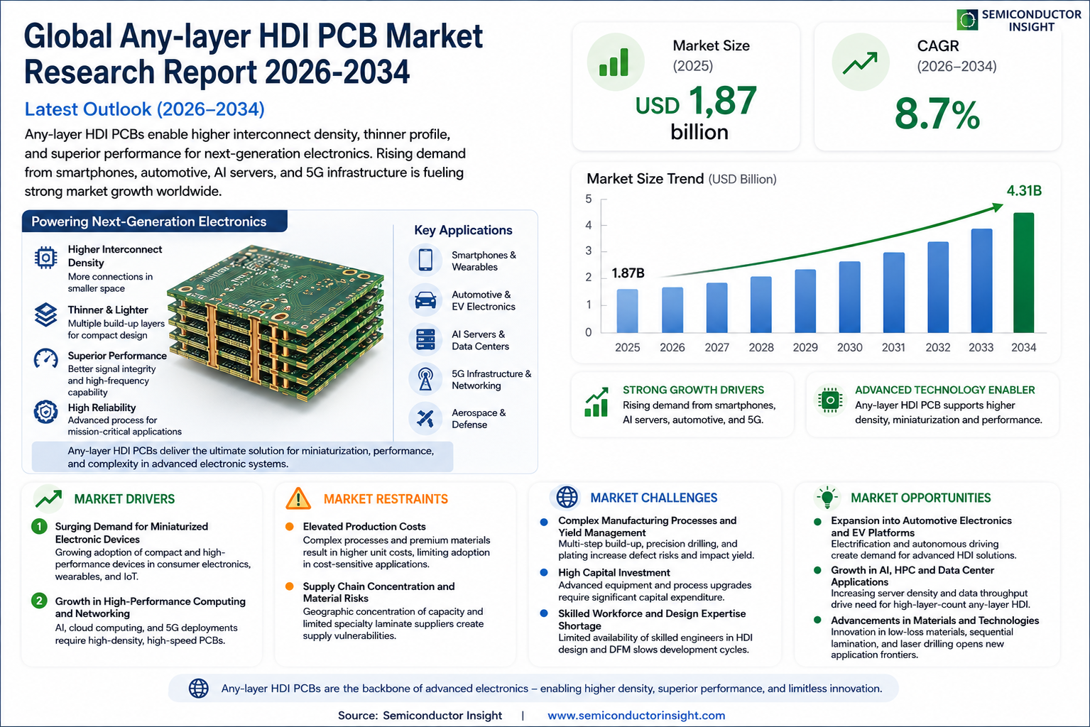
Global Any-layer HDI PCB market size was valued at USD 1.87 billion in 2025. The market is projected to grow from USD 2.04 billion in 2026 to USD 4.31 billion by 2034, exhibiting a CAGR of 8.7% during the forecast period.
Any-layer HDI PCB is an advanced high-density interconnect board manufactured using Anylayer interconnect technology, which enables connections between any two layers within a multi-layer printed circuit board (PCB). This sophisticated technology breaks through the conventional limitations of traditional HDI interlayer connections, significantly improving circuit board integration and overall performance. By allowing designers to freely route circuits within a constrained physical space, Anylayer HDI technology facilitates more complex, efficient, and compact circuit architectures — a capability increasingly critical in modern electronics manufacturing.
The market is witnessing robust growth driven by surging demand for miniaturized and high-performance electronics across consumer, automotive, and industrial sectors. The rapid proliferation of smartphones, wearables, and advanced driver-assistance systems (ADAS) has accelerated the adoption of Any-layer HDI PCBs. Furthermore, the expanding deployment of 5G infrastructure and the rise of Internet of Things (IoT) applications are compelling manufacturers to invest in higher-density, more reliable PCB technologies. Key global manufacturers operating in this space include MEIKO ELECTRONICS, Shennan Circuits, AKM Meadville, Aoshikang Technology, Founder Technology, Guangdong Goworld, Multek, iPCB, and Unitech PCB, among others, collectively shaping competitive dynamics across Global landscape.
MARKET DRIVERS
Rising Demand for Miniaturized and High-Performance Electronics
Any-layer HDI PCB market is witnessing robust expansion driven by the accelerating global demand for compact, lightweight, and high-performance electronic devices. As consumer electronics, telecommunications infrastructure, and automotive systems continue to evolve toward greater functional complexity within smaller form factors, any-layer HDI PCBs have emerged as a critical enabling technology. Unlike conventional HDI designs, any-layer interconnect structures allow vias to be placed between any two conductive layers, dramatically increasing routing density and enabling designers to achieve superior signal integrity in space-constrained applications. This architectural flexibility is particularly valuable for flagship smartphones, wearables, and advanced computing modules where board real estate is at a premium.
Proliferation of 5G Infrastructure and Advanced Semiconductor Packaging
Global rollout of 5G networks is a significant catalyst for Any-layer HDI PCB market. Base stations, small cells, and millimeter-wave antenna modules demand PCBs that can support high-frequency signal transmission with minimal loss, tight impedance control, and dense interconnection — attributes that any-layer HDI technology delivers with precision. Simultaneously, the semiconductor industry’s shift toward advanced packaging formats such as flip-chip BGA, system-in-package (SiP), and chiplet architectures requires substrate-level interconnect solutions where any-layer HDI structures play a foundational role. Leading chipmakers and ODMs are increasingly specifying any-layer HDI PCBs as mandatory for next-generation processor and memory module assemblies.
➤ The convergence of 5G deployment, AI-driven edge computing, and advanced semiconductor packaging is positioning any-layer HDI PCBs as an indispensable component in the electronics value chain, with design wins across tier-1 OEMs accelerating adoption throughout the forecast period.
The automotive sector represents another powerful demand driver for Any-layer HDI PCB market. The rapid electrification of vehicles and the integration of advanced driver-assistance systems (ADAS), LiDAR modules, and in-vehicle infotainment platforms are generating demand for PCBs that combine high reliability with exceptional interconnect density. Any-layer HDI designs support the fine-pitch component placement required by automotive-grade processors and radar chipsets, while also meeting stringent thermal and mechanical durability standards. As electric vehicle production scales globally, procurement of high-density interconnect substrates by Tier-1 automotive electronics suppliers is expected to intensify considerably.
MARKET CHALLENGES
Complex Manufacturing Processes and Yield Management
One of the foremost challenges confronting Any-layer HDI PCB market is the inherent complexity of the manufacturing process. Producing any-layer structures requires sequential lamination cycles, precision laser drilling for blind and buried microvias, and electroless copper deposition across multiple build-up layers — each step introducing potential sources of defect and yield loss. The tolerance stack-up across numerous lamination passes demands tightly controlled process environments and advanced inspection methodologies, including automated optical inspection (AOI) and X-ray tomography. Manufacturers operating at scale must invest substantially in process engineering and equipment calibration to maintain acceptable yield rates, which directly impacts production economics and delivery reliability for OEM customers.
Other Challenges
High Capital Investment Requirements
Establishing or upgrading fabrication capacity for any-layer HDI PCBs demands significant capital expenditure in laser drilling systems, direct imaging equipment, and advanced plating lines. For mid-tier fabricators, the financial barrier to entry constrains market participation and limits competitive dynamics, potentially creating supply concentration risks for buyers dependent on specialized any-layer HDI sourcing.
Skilled Workforce and Design Expertise Shortage
Any-layer HDI PCB market faces a persistent shortage of engineers proficient in high-density interconnect design rules, signal integrity simulation, and design-for-manufacturability (DFM) practices specific to any-layer architectures. As design complexity escalates with each new product generation, the gap between available talent and industry requirements poses a tangible constraint on market growth, particularly in regions where PCB engineering education has not kept pace with technology advancement.
MARKET RESTRAINTS
Elevated Production Costs Limiting Broader Market Penetration
Despite strong demand fundamentals, Any-layer HDI PCB market faces a significant restraint in the form of elevated unit production costs relative to conventional multilayer PCBs and standard HDI constructions. The sequential build-up process, high material consumption of specialty low-loss laminates and prepregs, and the capital intensity of microvia formation technologies collectively drive manufacturing cost structures that are substantially higher than traditional alternatives. While premium end markets such as flagship smartphones and aerospace-grade electronics can absorb these costs, the price sensitivity of mid-range consumer electronics and industrial applications remains a meaningful barrier to wider adoption of any-layer HDI solutions across a broader application spectrum.
Supply Chain Concentration and Raw Material Availability
Any-layer HDI PCB market is also restrained by a geographically concentrated supply chain, with the majority of advanced fabrication capacity situated in East Asia, particularly in Taiwan, South Korea, Japan, and mainland China. This concentration creates vulnerability to regional disruptions including geopolitical tensions, logistics bottlenecks, and natural events, as demonstrated by supply shocks experienced during recent global disruptions. Furthermore, the availability of specialty laminate materials — including ultra-low-loss dielectric substrates required for high-frequency any-layer HDI applications — is controlled by a limited number of qualified material suppliers, adding a procurement risk dimension that constrains the ability of PCB manufacturers to rapidly scale output in response to demand surges.
MARKET OPPORTUNITIES
Expansion into Automotive Electronics and Electric Vehicle Platforms
The accelerating global transition toward vehicle electrification and autonomous driving presents a compelling growth opportunity for Any-layer HDI PCB market. Automotive OEMs and Tier-1 suppliers are actively qualifying advanced PCB substrates capable of supporting the dense component integration required by battery management systems, power inverter control units, and centralized domain controller architectures prevalent in next-generation EV platforms. Any-layer HDI constructions offer the interconnect density, thermal performance, and long-term reliability demanded by automotive operating environments, positioning qualified manufacturers to capture growing design-win volumes as EV production ramps across North America, Europe, and Asia-Pacific through the coming years.
Growth in Wearable Medical Devices and Healthcare Electronics
The wearable medical device segment represents an emerging and high-value opportunity for Any-layer HDI PCB market. Continuous glucose monitors, cardiac rhythm management devices, neural stimulators, and next-generation hearing aids all require PCBs that deliver maximum functionality within extremely constrained dimensions — a requirement that any-layer HDI technology is uniquely positioned to address. Regulatory approvals for an expanding range of connected health monitoring devices, combined with aging global demographics and the increasing clinical acceptance of remote patient monitoring solutions, are expected to drive sustained procurement of miniaturized high-density PCBs by medical device manufacturers. This segment offers premium pricing potential and strong customer loyalty given the high qualification and compliance standards involved.
Artificial Intelligence Hardware and High-Performance Computing Applications
The explosive growth of artificial intelligence workloads and the corresponding build-out of data center infrastructure optimized for AI inference and training presents a substantial incremental opportunity for Any-layer HDI PCB market. AI accelerator cards, high-bandwidth memory modules, and optical interconnect interface boards increasingly rely on any-layer HDI substrates to achieve the interconnect densities required for multi-chip module integration and high-speed signal routing. As hyperscale data center operators and cloud service providers accelerate capital investment in AI infrastructure, demand for advanced PCB substrates with any-layer HDI capabilities is anticipated to grow meaningfully, offering PCB fabricators with the requisite process technology a strategically attractive avenue for revenue diversification and margin expansion.
MAIN TITLE HERE () Trends
Rising Demand for Miniaturized Electronics Driving Any-layer HDI PCB Market Adoption
Any-layer HDI PCB market is witnessing significant momentum as the electronics industry continues its shift toward smaller, more powerful, and highly integrated devices. Any-layer HDI PCB technology enables electrical connections between any two layers within a multi-layer printed circuit board, overcoming the traditional limitations of conventional HDI designs. This breakthrough allows engineers and circuit designers to optimize layouts within constrained physical spaces, supporting the development of compact yet high-performance electronic assemblies across a wide range of end-use sectors.
Consumer electronics remains one of the most influential demand drivers for Any-layer HDI PCB market. Smartphones, tablets, wearable devices, and ultra-thin laptops increasingly require circuit boards that support high-density interconnects without compromising reliability or signal integrity. The proliferation of 5G-enabled devices has further amplified design complexity, prompting manufacturers to adopt any-layer interconnect solutions that allow more flexible routing and reduced signal loss over shorter trace distances.
Other Trends
Automotive Electronics Integration
The automotive sector is emerging as a high-growth application area for Any-layer HDI PCB market. As vehicles incorporate advanced driver-assistance systems (ADAS), infotainment platforms, and electric powertrain controls, the need for compact and reliable circuit boards has intensified. Any-layer HDI technology supports the stringent performance and durability requirements of automotive-grade electronics, enabling automakers and Tier-1 suppliers to design more sophisticated electronic control units within tight spatial constraints.
Industrial and Medical Electronics Expansion
Industrial automation equipment and medical diagnostic devices are also contributing to growing demand within Any-layer HDI PCB market. In medical applications, miniaturized imaging systems, patient monitoring devices, and implantable electronics require boards with exceptional precision and high layer counts. Industrial use cases, including robotics, programmable logic controllers, and factory automation systems, similarly benefit from the enhanced interconnect density and design flexibility that any-layer technology provides.
Asia-Pacific Leading Regional Growth with Strong Manufacturing Base
Asia-Pacific continues to dominate Any-layer HDI PCB market, driven by a robust electronics manufacturing ecosystem concentrated in China, Japan, South Korea, and Southeast Asia. China, in particular, hosts several of the world’s leading Any-layer HDI PCB manufacturers, including Shennan Circuits, Aoshikang Technology, Founder Technology, and Guangdong Goworld, among others. The region benefits from integrated supply chains, cost-competitive production capacity, and sustained investments in advanced PCB fabrication technologies. Meanwhile, North America and Europe are registering steady demand, particularly from automotive, aerospace, and industrial electronics segments, where high-reliability PCB solutions are essential for mission-critical applications.
COMPETITIVE LANDSCAPE
Key Industry Players
Any-layer HDI PCB Market – Competitive Dynamics, Key Manufacturers, and Strategic Positioning
Global Any-layer HDI PCB market is characterized by intense competition among a concentrated group of technologically advanced manufacturers, predominantly headquartered in Asia, with significant influence from Japanese, Chinese, and Taiwanese players. MEIKO ELECTRONICS stands out as one of the foremost leaders in the any-layer HDI PCB space, leveraging decades of precision manufacturing expertise and a robust R&D pipeline to maintain a dominant share in high-end applications such as smartphones, wearables, and advanced automotive electronics. Shennan Circuits and AKM Meadville also command substantial market presence, with their vertically integrated production capabilities and strategic partnerships with global OEMs enabling them to serve high-volume consumer electronics and industrial segments efficiently. The top five players collectively accounted for a significant portion of global revenue in 2025, underscoring the market’s moderately consolidated structure. Competition is primarily driven by technological differentiation — specifically, the ability to deliver fine-line circuitry, laser-drilled microvias, and reliable interlayer connectivity across 10-layer and 12-layer any-layer HDI configurations — alongside cost competitiveness, yield optimization, and speed-to-market capabilities.
Beyond the leading incumbents, several regionally significant and niche players are actively expanding their footprint in Any-layer HDI PCB market. Aoshikang Technology and Founder Technology have emerged as strong contenders within China’s rapidly scaling PCB ecosystem, benefiting from domestic demand in consumer electronics and government-backed initiatives supporting advanced electronics manufacturing. Guangdong Goworld and Unitech PCB continue to carve out competitive positions through capacity expansions and investments in automated production lines, particularly targeting the automotive electronics and industrial segments. Multek, with its global manufacturing network, caters to high-reliability applications, while iPCB focuses on agile, quick-turn solutions for smaller-volume, high-complexity orders. As miniaturization trends intensify and demand for any-layer interconnect technology accelerates across applications including 5G devices, ADAS systems, and medical electronics, competitive pressure is expected to mount further, compelling players to invest aggressively in advanced process technologies, strategic alliances, and geographic diversification to sustain and grow their market positions through 2034.
List of Key Any-layer HDI PCB Companies Profiled
- MEIKO ELECTRONICS
- Shennan Circuits
- AKM Meadville
- Aoshikang Technology
- Founder Technology
- Guangdong Goworld
- Multek
- iPCB
- Unitech PCB
- TTM Technologies
- Tripod Technology Corporation
- Compeq Manufacturing
- AT&S (Austria Technologie & Systemtechnik)
- Ibiden Co., Ltd.
- Unimicron Technology Corporation
Segment Analysis:
| Segment Category | Sub-Segments | Key Insights |
| By Type |
|
10 Layer boards represent the leading segment in Any-layer HDI PCB market, driven by their optimal balance between design complexity and manufacturing feasibility.
|
| By Application |
|
Consumer Electronics stands as the dominant application segment, propelled by the relentless demand for thinner, lighter, and more powerful devices across global markets.
|
| By End User |
|
OEMs (Original Equipment Manufacturers) represent the largest end-user group in Any-layer HDI PCB market, as they drive design specifications and procurement volumes across consumer, automotive, and industrial sectors.
|
| By Technology |
|
Laser Drilling Technology is the leading manufacturing technology segment underpinning Any-layer HDI PCB market, enabling the formation of ultra-fine microvias that are essential to achieving the high interconnect densities demanded by modern electronics.
|
| By Region |
|
Asia Pacific dominates Global Any-layer HDI PCB market, anchored by the manufacturing powerhouses of China, Japan, South Korea, and Southeast Asia, which together host a dense concentration of leading PCB fabricators and their downstream electronics customers.
|
Regional Analysis: Any-layer HDI PCB Market
Asia-Pacific
Asia-Pacific hosts the world’s most advanced any-layer HDI PCB manufacturing clusters, with facilities in Japan, Taiwan, and South Korea operating at the frontier of precision fabrication. These nations have cultivated decades of process expertise, enabling consistent production of ultra-fine line widths and via structures that meet the stringent demands of next-generation consumer and industrial electronics applications.
The region’s insatiable appetite for smartphones, tablets, advanced wearables, and automotive electronics creates a self-sustaining demand cycle for any-layer HDI PCB solutions. Major consumer electronics brands headquartered or assembled across Asia-Pacific continuously push design boundaries, requiring increasingly complex board architectures that only any-layer HDI technology can reliably deliver at scale.
Governments across Asia-Pacific have introduced targeted industrial policies, subsidies, and technology grants aimed at strengthening domestic advanced PCB capabilities. These initiatives reduce dependence on imported substrates and materials while encouraging local innovation. Strategic investments in research infrastructure and workforce development are steadily elevating the regional any-layer HDI PCB market’s technical sophistication and global competitiveness.
One of Asia-Pacific’s most formidable advantages in Any-layer HDI PCB market is its vertically integrated supply chain, spanning specialty laminates, laser drilling equipment, chemical processes, and finished board assembly. This integration reduces lead times, lowers production costs, and enables rapid design iteration — critical factors for electronics brands competing in fast-moving, innovation-driven global markets.
North America
North America represents a strategically significant region in Any-layer HDI PCB market, distinguished by its concentration of high-value end-use industries including aerospace and defense, advanced medical devices, and high-performance computing. The United States in particular drives demand for ruggedized, high-reliability any-layer HDI PCB solutions that meet stringent military and medical certifications. While large-scale volume manufacturing has largely migrated to Asia, North American fabricators have carved a sustainable niche by specializing in low-to-medium volume, technologically complex orders where precision and compliance outweigh cost considerations. Growing domestic initiatives to reshore critical electronics manufacturing, combined with increasing defense and semiconductor-related government spending, are gradually expanding the regional manufacturing base. The proliferation of electric vehicles, 5G network infrastructure, and data center expansion further amplifies demand for advanced any-layer HDI PCB technologies across the region through the forecast period.
Europe
Europe occupies a measured yet increasingly relevant position in Global any-layer HDI PCB market, anchored by robust demand from the automotive, industrial automation, and telecommunications sectors. Germany, Switzerland, and the Nordic countries are particularly active in deploying any-layer HDI PCB technology within precision engineering and automotive electronics applications, where reliability and thermal performance are paramount. European manufacturers are increasingly prioritizing sustainability, pushing suppliers and fabricators toward environmentally responsible materials and production processes — a dynamic that is reshaping procurement strategies across the any-layer HDI PCB supply chain. The region’s strong regulatory environment and focus on quality certification encourage the adoption of advanced interconnect solutions. Strategic partnerships between European automotive OEMs and PCB technology providers are expected to sustain steady market expansion through 2034, particularly as electrification and autonomous vehicle development accelerate.
South America
South America remains an emerging participant in Any-layer HDI PCB market, with growth primarily concentrated in Brazil and, to a lesser extent, Mexico and Argentina. The region’s electronics manufacturing sector is developing gradually, supported by government-backed industrial programs aimed at reducing import dependence and stimulating local technology production. Demand for any-layer HDI PCBs in South America is largely driven by the telecommunications, consumer electronics, and energy sectors, with increasing interest from automotive assembly operations. While the region currently relies heavily on imports from Asia-Pacific and North America for advanced PCB solutions, rising foreign direct investment and improving technical education infrastructure are laying the groundwork for longer-term manufacturing capability development. Any-layer HDI PCB market in South America is expected to evolve steadily as industrial modernization initiatives gain traction across the forecast period.
Middle East & Africa
The Middle East and Africa represent nascent but forward-looking markets within the broader any-layer HDI PCB landscape. Demand in this region is primarily driven by telecommunications infrastructure expansion, government-led smart city initiatives, and growing investments in defense and security electronics. Gulf Cooperation Council nations, particularly the UAE and Saudi Arabia, are channeling substantial resources into technology diversification as part of broader economic transformation agendas, creating indirect demand for advanced PCB solutions including any-layer HDI technology. Africa’s contribution remains limited by infrastructure constraints and early-stage electronics manufacturing ecosystems, though select markets show promise as mobile connectivity and industrial digitalization expand. Over the forecast period to 2034, increasing technology adoption, regional data center development, and cross-border trade agreements are expected to gradually elevate the Middle East and Africa’s role in Global any-layer HDI PCB market.
Report Scope
This market research report provides a comprehensive analysis of Any-layer HDI PCB market, covering the forecast period 2026–2034. It offers detailed insights into market dynamics, technological advancements, competitive landscape, and key trends shaping the industry.
Key focus areas of the report include:
- Market Overview: The report begins with an overview outlining its current market scenario, key growth indicators, and industry transformation drivers. It discusses macroeconomic factors, demand–supply balance, regulatory landscape, and the strategic role of Any-layer HDI PCB technology in powering advancements across industries such as automotive electronics, telecommunications, consumer electronics, and industrial automation.
- Market Size & Forecast: Historical data and future projections for revenue, unit shipments, and market value across major regions and segments.
- Segmentation Analysis: Detailed breakdown by product type (10 Layer, 12 Layer, Other), application, and end-user industry to identify high-growth segments and investment opportunities.
- Regional Insights: Insights into market performance across North America, Europe, Asia-Pacific, Latin America, and the Middle East & Africa, including country-level analysis where relevant.
- Competitive Landscape: Profiles of leading market participants, including their product offerings, R&D focus, manufacturing capacity, pricing strategies, and recent developments such as mergers, acquisitions, and partnerships.
- Technology Trends & Innovation: Assessment of emerging technologies, integration of AI/IoT, Anylayer interconnect design trends, fabrication techniques, and evolving industry standards.
- Market Drivers & Restraints: Evaluation of factors driving market growth along with challenges, supply chain constraints, regulatory issues, and market-entry barriers.
- Stakeholder Insights: Insights for component suppliers, OEMs, system integrators, investors, and policymakers regarding the evolving ecosystem and strategic opportunities.
Primary and secondary research methods are employed, including interviews with industry experts, data from verified sources, and real-time market intelligence to ensure the accuracy and reliability of the insights presented.
FREQUENTLY ASKED QUESTIONS:
What is the current market size of Any-layer HDI PCB Market?
-> Global Any-layer HDI PCB Market was valued at USD 1.87 billion in 2025 and is expected to reach USD 4.31 billion by 2034, growing at a CAGR of 8.7% during the forecast period.
Which key companies operate in Any-layer HDI PCB Market?
-> Key players include MEIKO ELECTRONICS, Shennan Circuits, AKM Meadville, Aoshikang Technology, Founder Technology, Guangdong Goworld, Multek, iPCB, and Unitech PCB, among others. In 2025, Global top five players held approximately % of the market in terms of revenue.
What are the key growth drivers?
-> Key growth drivers include rising demand for high-density interconnect solutions in consumer electronics and automotive electronics, increasing adoption of Anylayer interconnect technology enabling complex multi-layer circuit designs, and growing requirements for miniaturized and high-performance PCBs across industrial and medical applications.
Which region dominates the market?
-> Asia is a dominant and fastest-growing region in Any-layer HDI PCB market, with China projected to reach USD million and the U.S. market estimated at USD million in 2025. Key manufacturing hubs are concentrated across China, Japan, South Korea, and Southeast Asia.
What are the emerging trends?
-> Emerging trends include adoption of Anylayer HDI technology for ultra-compact circuit designs, increasing use of 10 Layer and 12 Layer HDI boards in advanced applications, growing integration of HDI PCBs in automotive electronics and industrial/medical devices, and rising demand for high-integration, high-performance printed circuit boards driven by miniaturization trends across the electronics industry.

Get Sample Report PDF for Exclusive Insights
Report Sample Includes
- Table of Contents
- List of Tables & Figures
- Charts, Research Methodology, and more...
 Download Sample Report PDF