AI Thin Film Stress Measurement Wafer Curvature Analysis Chip Market Insights
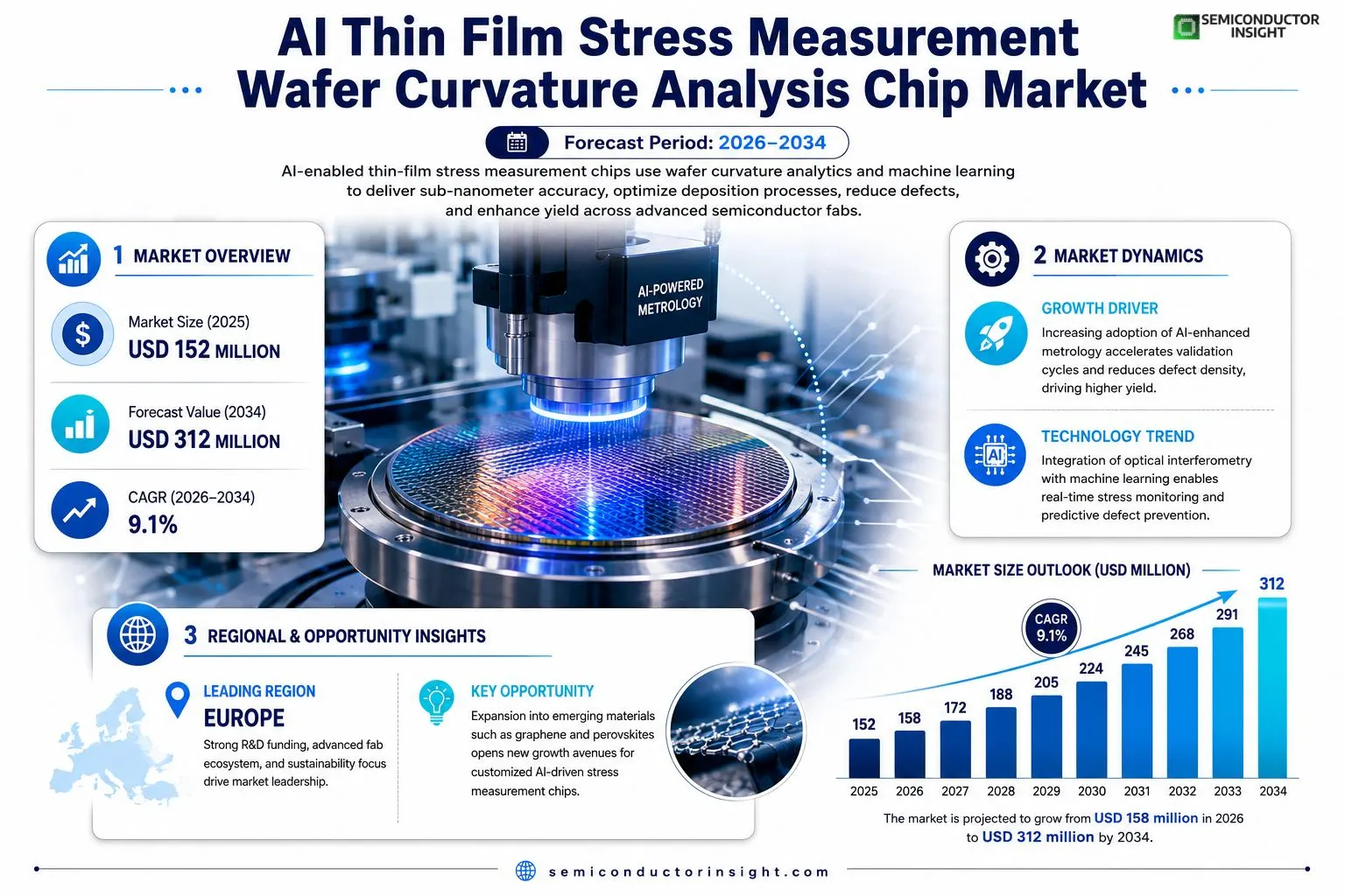
AI Thin Film Stress Measurement Wafer Curvature Analysis Chip market size was valued at USD 152 million in 2025. The market is projected to grow from USD 158 million in 2026 to USD 312 million by 2034, exhibiting a CAGR of 9.1% during the forecast period.
AI‑enabled thin‑film stress measurement chips are specialized semiconductor devices that quantify wafer curvature to infer intrinsic stress in deposited layers. By integrating optical interferometry with machine‑learning algorithms, these chips deliver sub‑nanometer resolution and real‑time analytics, enabling manufacturers to optimize deposition processes, reduce defect density, and improve yield across advanced CMOS, MEMS, and photonic foundries.The market is experiencing rapid growth because semiconductor fabs are scaling to sub‑3 nm nodes, which demand tighter stress control. Furthermore, rising adoption of AI‑driven predictive maintenance in fabs accelerates demand for such chips. However, high capital expenditure for equipment upgrades poses a challenge for smaller fabs. Leading players such as KLA Corporation, Applied Materials, and Nanometrics are expanding their portfolios through strategic acquisitions and collaborationse.g., KLA’s partnership with IBM in March 2024 to integrate quantum‑enhanced analytics into curvature sensorsfueling further expansion.
MARKET DRIVERS
Increasing Adoption of AI‑Enhanced Metrology
The integration of artificial intelligence into thin‑film stress measurement has accelerated validation cycles, enabling manufacturers to achieve up to 30% faster time‑to‑market. This efficiency gain is a primary catalyst for AI Thin Film Stress Measurement Wafer Curvature Analysis Chip Market, as semiconductor fabs seek higher throughput.
Rising Demand for Miniaturized Sensors
Compact curvature analysis chips are replacing bulkier optical setups, allowing integration directly onto production lines. Analysts project a compound annual growth rate of 12% driven by this shift toward in‑situ monitoring.
➤ AI algorithms now predict film delamination before it occurs, reducing scrap rates by up to 18%.
These predictive capabilities, combined with lower equipment cost, are strengthening supplier confidence and prompting new capital expenditures across major foundries.
MARKET CHALLENGES
Data Integration Complexity
Legacy manufacturing execution systems often lack the interfaces needed to ingest real‑time curvature data, creating bottlenecks that hinder full AI utilization. Companies must invest in middleware to bridge this gap.
Other Challenges
High Initial Investment
The upfront cost of AI‑enabled chips and supporting analytics platforms can exceed $500k for a mid‑size fab, which may delay adoption among cost‑sensitive operators.
MARKET RESTRAINTS
Regulatory and Qualification Barriers
Stringent qualification standards for metrology equipment in aerospace and automotive sectors add lengthy approval cycles. This slows market penetration despite clear performance advantages.Furthermore, the requirement for extensive calibration against reference wafers increases operational overhead, limiting scalability for smaller enterprises.
MARKET OPPORTUNITIES
Expansion into Emerging Materials
New material systems such as graphene and perovskites demand precise stress monitoring. AI Thin Film Stress Measurement Wafer Curvature Analysis Chip Market is uniquely positioned to serve these niches, offering customized algorithms that account for anisotropic curvature behavior.Strategic partnerships with material research institutes are expected to unlock additional revenue streams, as bespoke chip designs become integral to next‑generation device fabrication.
AI Thin Film Stress Measurement Wafer Curvature Analysis Chip Market Trends
AI‑Enabled Stress Measurement Gains Broad Adoption
AI Thin Film Stress Measurement Wafer Curvature Analysis Chip Market is witnessing accelerated uptake as semiconductor manufacturers target sub‑3 nm process nodes. Tight control of wafer curvature has become essential to maintain device reliability, and AI‑driven analytics embedded in the chips enable real‑time correction of deposition parameters. Leading foundries are deploying these sensors to lower defect density and improve overall yield, leveraging the combination of optical interferometry and adaptive machine‑learning models. Recent collaborations, such as the partnership between KLA Corporation and IBM to integrate quantum‑enhanced analytics into curvature sensors, exemplify how the market is moving toward increasingly sophisticated predictive capabilities.
Other Trends
Integration of Optical Interferometry with Machine Learning
Modern stress‑measurement chips combine sub‑nanometer optical interferometry with AI algorithms that continuously learn from process data. This fusion delivers unprecedented resolution and facilitates automated process adjustments without manual intervention. The result is a closed‑loop control system that shortens cycle times and reduces the need for costly trial‑and‑error experiments. Manufacturers report measurable improvements in yield consistency, especially in advanced CMOS, MEMS, and photonic platforms where stress gradients can critically affect performance.
Capital Investment and Competitive Landscape
A notable challenge for AI Thin Film Stress Measurement Wafer Curvature Analysis Chip Market is the high capital outlay required for equipment upgrades and sensor integration. Smaller fabs often face budgeting constraints, which can slow adoption despite clear technical benefits. Nevertheless, major players such as Applied Materials, Nanometrics, and KLA continue to expand their portfolios through strategic acquisitions and joint development programs. These activities foster a competitive environment that drives innovation and gradually reduces entry barriers, encouraging broader market participation over the next several years.
COMPETITIVE LANDSCAPE
Key Industry Players
AI Thin Film Stress Measurement Wafer Curvature Analysis Chip Market – Competitive Overview
The AI‑enabled thin‑film stress measurement segment is dominated by a few semiconductor metrology leaders that have integrated advanced optics with machine‑learning analytics. KLA Corporation leverages its deep wafer inspection heritage and recently expanded its curvature‑sensor portfolio through a partnership with IBM to embed quantum‑enhanced analytics, positioning it as the de‑facto standard for sub‑nanometer stress monitoring. Applied Materials complements its equipment base with AI‑driven metrology modules that feed directly into deposition tool controls, reinforcing its cross‑portfolio advantage. Nanometrics, now part of Onto Innovation, continues to differentiate through high‑resolution interferometric chips that support predictive maintenance across 3 nm and smaller nodes, thereby shaping the market’s consolidation trajectory and setting pricing benchmarks for the emerging chip ecosystem.Beyond the tier‑one trio, a broader set of niche players contributes critical depth and specialization. ASML’s metrology arm offers complementary curvature diagnostics integrated with lithography platforms, while Tokyo Electron supplies AI‑augmented wafer inspection solutions to Asian fabs. Hitachi High‑Technologies, Advantest, and Lam Research deliver sensor‑centric modules that address MEMS and photonic foundry needs. Emerging innovators such as Nova Measuring Instruments, Bruker, and Rudolph Technologies (under Onto) focus on low‑cost, high‑throughput curvature analysis for mid‑size fabs. Together, these companies create a competitive mosaic that balances scale, AI capability, and application‑specific expertise, driving adoption despite the high capital outlay required for full‑system upgrades.
List of Key AI Thin Film Stress Measurement Wafer Curvature Analysis Chip Companies Profiled
- KLA Corporation
- Applied Materials
- Advantest
- Lam Research
- Nova Measuring Instruments
- Bruker
- Rudolph
Segment Analysis:
| Segment Category | Sub-Segments | Key Insights |
| By Type |
|
Optical‑Interferometry Based Chips are viewed as the leading type because they combine proven interferometric precision with machine‑learning driven curvature interpretation. • They enable sub‑nanometer curvature detection, allowing fabs to fine‑tune stress control at sub‑3 nm nodes. • Integration with AI delivers predictive alerts on stress‑induced defects before they propagate. • Their proven reliability makes them the first choice for high‑volume CMOS and photonic foundries seeking tight process windows. |
| By Application |
|
Advanced CMOS Node Calibration dominates application relevance as wafer curvature insights directly influence lithography overlay and stress‑aware patterning. • AI‑driven curvature analytics feed back into deposition recipes, reducing defect generation. • The capability to monitor stress in real time supports rapid “try‑and‑learn” cycles essential for sub‑3 nm process development. • Foundries value the seamless integration with existing process control software, fostering a unified data ecosystem. |
| By End User |
|
Semiconductor Foundries are the primary end‑user segment, driven by the need for ultra‑precise stress control in next‑generation node production. • Foundries adopt AI‑enabled curvature chips to embed predictive maintenance within the fab, reducing unplanned downtime. • The technology aligns with their broader digital‑twin initiatives, enhancing overall yield management. • Collaboration between chip vendors and AI specialists creates a feedback loop that continuously refines stress models. |
| By Integration Architecture |
|
Embedded Wafer‑Scale Controllers are emerging as the most influential architecture because they allow curvature data to be processed directly on the wafer, shortening decision latency. • On‑chip AI models adapt to local process variations without relying on external computation. • This architecture supports seamless integration with existing fab automation frameworks, enhancing overall process transparency. • Industry leaders are investing in modular designs that can be retrofitted to legacy equipment, accelerating adoption. |
| By Value Chain Position |
|
Equipment OEMs drive the segment because they embed the chips into deposition and metrology tools, shaping how stress data is captured. • OEMs collaborate closely with AI firms to embed analytics, creating differentiated tool offerings. • Their influence extends to standards development for curvature data formats, fostering ecosystem interoperability. • Strategic partnerships, such as KLA’s alliance with IBM, illustrate how OEMs leverage AI expertise to enhance sensor capabilities. |
Regional Analysis: AI Thin Film Stress Measurement Wafer Curvature Analysis Chip Market
Europe
The European Union’s semiconductor sustainability directives incentivize the deployment of AI‑driven stress monitoring, prompting manufacturers to adopt chips that provide accurate curvature analytics while minimizing chemical usage in wafer processing.
Leading equipment suppliers are forming joint ventures with AI start‑ups, co‑creating wafer curvature analysis solutions that embed machine‑learning models for instant defect prediction across EU fabs.
European fabs are piloting edge‑AI chips that combine optical interferometry with deep‑learning inference, achieving sub‑nanometer stress resolution and reducing cycle times for thin‑film processes.
A resilient supply chain backed by EU‑wide strategic stockpiles ensures steady availability of AI‑enabled measurement components, mitigating disruptions that could affect wafer curvature analysis production.
North America
North America’s market is shaped by the United States’ focus on advanced node development and substantial venture capital backing for AI‑centric metrology startups. Industry consortia are standardizing data formats for curvature analysis, fostering interoperability across toolchains. While the region benefits from a large customer base, it faces pressure to lower latency in AI inference, driving interest in on‑chip processing solutions that enhance wafer stress monitoring without cloud dependence.
Asia‑Pacific
In the Asia‑Pacific, rapid fab expansion in China, South Korea, and Taiwan fuels demand for AI Thin Film Stress Measurement solutions that can keep pace with high‑volume production. Regional manufacturers prioritize cost‑effective chips with robust AI models to manage stress in dense multi‑layer stacks. Government incentives for smart manufacturing further accelerate adoption, though intellectual property considerations remain a strategic challenge.
South America
South America’s semiconductor activity is emerging, with Brazil and Argentina investing in pilot lines that incorporate AI‑enabled curvature analysis for specialized thin‑film applications. Market growth is modest but driven by academic‑industry collaborations that aim to build local expertise in AI‑based metrology, positioning the region for incremental market entry in the coming decade.
Middle East & Africa
The Middle East & Africa region is witnessing early-stage interest as nations diversify economies beyond oil and gas. Initiatives in the United Arab Emirates and South Africa focus on establishing research hubs that explore AI‑integrated wafer stress measurement, targeting niche markets such as aerospace and renewable energy where thin‑film reliability is critical.
Report Scope
This market research report provides a comprehensive analysis of the AI Thin Film Stress Measurement Wafer Curvature Analysis Chip Market , covering the forecast period 2026–2034. It offers detailed insights into market dynamics, technological advancements, competitive landscape, and key trends shaping the industry.
Key focus areas of the report include:
- Market Overview: The report begins with an overview outlining its current market scenario, key growth indicators, and industry transformation drivers. It discusses macroeconomic factors, demand–supply balance, regulatory landscape, and the strategic role of semiconductors in powering advancements across industries such as automotive, telecommunications, consumer electronics, and industrial automation.
- Market Size & Forecast: Historical data and future projections for revenue, unit shipments, and market value across major regions and segments.
- Segmentation Analysis: Detailed breakdown by product type, technology, application, and end-user industry to identify high-growth segments and investment opportunities.
- Regional Insights: Insights into market performance across North America, Europe, Asia-Pacific, Latin America, and the Middle East & Africa, including country-level analysis where relevant.
- Competitive Landscape: Profiles of leading market participants, including their product offerings, R&D focus, manufacturing capacity, pricing strategies, and recent developments such as mergers, acquisitions, and partnerships.
- Technology Trends & Innovation: Assessment of emerging technologies, integration of AI/IoT, semiconductor design trends, fabrication techniques, and evolving industry standards.
- Market Drivers & Restraints: Evaluation of factors driving market growth along with challenges, supply chain constraints, regulatory issues, and market-entry barriers.
- Stakeholder Insights: Insights for component suppliers, OEMs, system integrators, investors, and policymakers regarding the evolving ecosystem and strategic opportunities.
Primary and secondary research methods are employed, including interviews with industry experts, data from verified sources, and real-time market intelligence to ensure the accuracy and reliability of the insights presented.
FREQUENTLY ASKED QUESTIONS:
What is the current market size of AI Thin Film Stress Measurement Wafer Curvature Analysis Chip Market?
-> AI Thin Film Stress Measurement Wafer Curvature Analysis Chip Market was valued at USD 152 million in 2025 and is expected to reach USD 312 million by 2034.
Which key companies operate in AI Thin Film Stress Measurement Wafer Curvature Analysis Chip Market?
-> Key players include KLA Corporation, Applied Materials, and Nanometrics, among others.
What are the key growth drivers?
-> Key growth drivers include scaling of semiconductor fabs to sub‑3 nm nodes, tighter wafer stress control requirements, and AI‑driven predictive maintenance adoption.
Which region dominates the market?
-> The market sees strong adoption worldwide, with notable activity in North America, Europe, and Asia‑Pacific where leading fabs are concentrated.
What are the emerging trends?
-> Emerging trends include integration of machine‑learning algorithms with optical interferometry, real‑time analytics for stress monitoring, and quantum‑enhanced analytics collaborations such as the KLA‑IBM partnership.
Get Sample Report PDF for Exclusive Insights
Report Sample Includes
- Table of Contents
- List of Tables & Figures
- Charts, Research Methodology, and more...