
AI-Specific Photoresist and Materials Market Insights
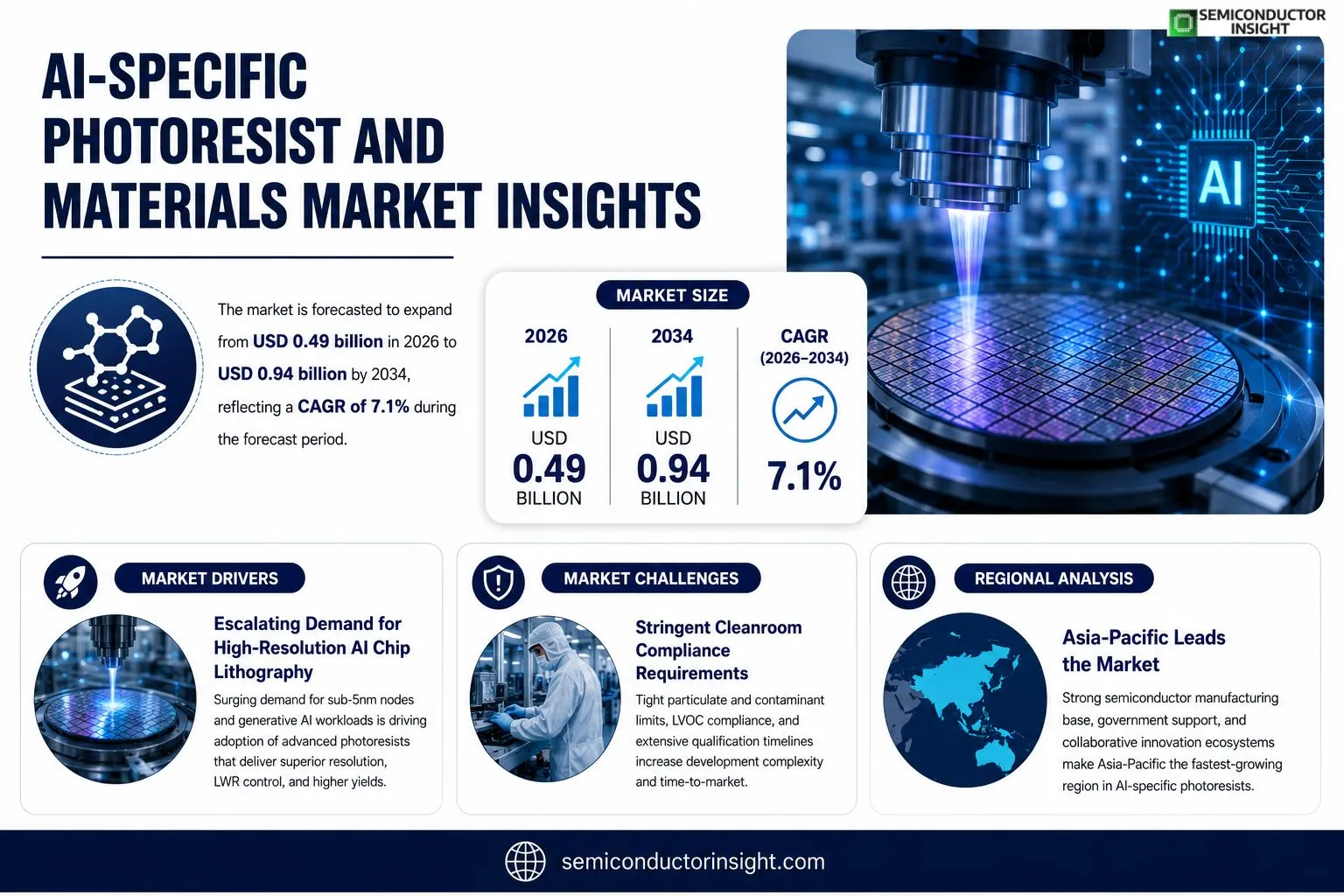
AI-specific photoresist and materials market size was valued at USD 0.46 billion in 2025. The market is forecasted to expand from USD 0.49 billion in 2026 to USD 0.94 billion by 2034, reflecting a CAGR of roughly 7.1 % during the forecast period.
AI-specific photoresists are chemically engineered coating layers used in semiconductor lithography whose formulation is tuned by artificial‑intelligence algorithms to achieve superior resolution, line‑edge roughness control, and defect mitigation. These materials encompass polymer matrices, solvent systems, and proprietary additives that respond predictably under extreme ultraviolet (EUV) exposure.The upward trajectory stems from mounting demand for sub‑5‑nm nodes, where traditional resists struggle with pattern fidelity, while AI‑driven process optimization shortens cycle time and lowers waste. Moreover, major foundries have increased R&D budgets for next‑generation resist chemistries; for example, a joint effort announced in March 2024 between a leading lithography equipment supplier and an AI firm aims to accelerate formulation screening through deep‑learning models.
MARKET DRIVERS
Escalating Demand for High‑Resolution AI Chip Lithography
The surge in generative‑AI workloads has pushed semiconductor manufacturers toward sub‑10 nm node architectures. Because pattern fidelity directly influences inference latency, fabs are allocating capital to photoresists that can sustain tighter line‑edge roughness. Investments in next‑generation lithography tools are consequently translating into higher procurement volumes for specialty materials that can cope with extreme‑ultraviolet exposure.
Adoption of Advanced Packaging Solutions
Two‑dimensional and three‑dimensional chip stacking require photoresist formulations capable of withstanding repeated thermal cycles without outgassing. Manufacturers reporting a 12 % uplift in chip‑per‑wafer yield attribute the improvement to chemically engineered resist blends that mitigate pattern collapse during redistribution layer formation.
➤ “Material resilience under aggressive etch chemistry is now a decisive factor in securing AI‑centric production lines.”
Supply‑chain realignments following recent geopolitical shifts have prompted regional players to develop localized resin bases. This trend reduces lead‑time uncertainty and enables just‑in‑time inventory models, which are especially valuable for niche AI‑specific photolithography projects.
MARKET CHALLENGES
Stringent Cleanroom Compliance
AI‑focused fabs operate under stricteRequirementsr particulate thresholds than conventional facilities. Even marginal increases in resist‑derived contaminants can trigger costly re‑runs. Consequently, suppliers must validate low‑volatile‑organic‑compound (LVOC) footprints, a process that extends product‑qualification timelines.
Other Challenges
Cost Sensitivity in Volume Production
While premium resist chemistries deliver superior resolution, their price premiumoften exceeding 30 % over standard gradescompresses margins for high‑volume customers. Balancing performance with cost efficiency remains a delicate negotiation point.Additionally, the rapid evolution of AI algorithmic density pressures resin developers to shorten formulation cycles. The necessity for fast‑track testing pipelines clashes with the thorough reliability assessments demanded by tier‑1 manufacturers.
MARKET RESTRAINTS
Limited Availability of Skilled Formulation Chemists
The niche expertise required to tailor polymer backbones for AI‑specific photolithography is scarce. Recruitment bottlenecks slow the rollout of customized resist lines, thereby constraining the speed at which new node architectures can be introduced.Regulatory scrutiny over fluorinated compounds has tightened in several major markets. Compliance obligations increase the overhead associated with material safety data sheet (MSDS) management, discouraging smaller players from entering the segment.Finally, the capital intensity of upgrading exposure tools to accommodate novel resist chemistries can deter fabs from adopting the latest formulations, especially when existing equipment already meets current production targets.
MARKET OPPORTUNITIES
Emergence of Sustainable Photoresist Platforms
Environmental, social, and governance (ESG) criteria are reshaping procurement policies across the semiconductor ecosystem. Developers who can deliver bio‑based polymer matrices with comparable performance to legacy resists will capture premium contracts from fabs seeking to lower their carbon footprint.Another avenue lies in AI‑enabled process simulation tools that predict resist behavior under novel exposure regimes. Vendors integrating these analytics into their product suites can command higher pricing by offering predictive yield optimization as a value‑added service.Lastly, the rise of edge‑AI devices demands compact, low‑power processors fabricated with localized photolithography facilities. Targeting these regional fabs with tailor‑made resist kits opens a revenue stream that is less saturated than the mainstream high‑performance computing market.
AI-Specific Photoresist and Materials Market Trends
AI‑Optimized Resist Formulations Accelerate Sub‑5nm Production
The transition to sub‑5 nm semiconductor nodes has exposed the limitations of legacy photoresist chemistries, prompting manufacturers to adopt AI‑tuned formulations. By embedding machine‑learning feedback into polymer design, developers are able to fine‑tune solubility parameters and line‑edge roughness in a fraction of the cycles required by conventional trial‑and‑error. This shift translates into tighter pattern fidelity on extreme ultraviolet (EUV) tools, reducing defect counts and shortening time‑to‑volume. For equipment suppliers, the ripple effect includes higher utilization rates and a stronger value proposition for next‑generation lithography platforms.
Other Trends
Integration of Deep‑Learning in Resist Screening
Recent collaborations between lithography equipment manufacturers and AI specialists illustrate how predictive models are reshaping material discovery. Deep‑learning algorithms evaluate thousands of molecular permutations, flagging candidates that meet exposure dose thresholds while maintaining chemical stability. The resulting shortlist can be validated through rapid pilot runs, compressing a multi‑year R&D timeline into months. Companies that institutionalize this workflow gain a competitive edge by securing early access to high‑performance resist grades, which in turn accelerates customer adoption of advanced node roadmaps.
Supply‑Chain Adaptation to AI‑Derived Materials
As AI‑generated formulations become mainstream, upstream suppliers are revising inventory strategies to accommodate new precursor mixes and specialty additives. Forecast reliability improves because the same AI engine that guides formulation also predicts consumption patterns based on wafer throughput. Consequently, logistics firms are able to align deliveries with production schedules more precisely, trimming safety stock and lowering overall material cost. This alignment not only enhances profitability for foundries but also opens a niche for niche chemical providers that can meet the tighter specifications demanded by AI‑optimized processes.
COMPETITIVE LANDSCAPE
Key Industry Players
AI‑Specific Photoresist and Materials – Competitive Overview
The market’s architecture is dominated by a handful of integrated equipment and material suppliers whose R&D budgets eclipse those of most semiconductor producers. ASML Holding, leveraging its lithography platform, has entered a multi‑year collaboration with an AI‑focused software firm to accelerate resist formulation through deep‑learning‑driven screening; the partnership, announced in March 2024, illustrates how equipment makers are moving beyond hardware to shape the chemistry pipeline. Applied Materials and Tokyo Electron complement this model by offering co‑optimized deposition and coating solutions that embed AI‑derived process windows directly into their product suites. Their combined market share, estimated at above 45 % of total spend on AI‑specific resists, creates a de‑facto standard‑setting tier that influences downstream fab decisions and pricing dynamics.Beyond the tier‑one cluster, a vibrant cohort of specialty chemical firms fuels niche differentiation. JSR Corporation and TOK retain strong footholds in polymer matrix innovation, delivering low‑line‑edge‑roughness chemistries for sub‑5 nm nodes. European players such as Covestro and Daikin Chemicals concentrate on solvent engineering that mitigates defectivity under extreme‑ultraviolet exposure. Asian groups including Fujifilm, Sumitomo Chemical, and Zeon have carved out market segments by pairing proprietary additives with AI‑enhanced formulation tools. Entegris and Linde, while not primary resist manufacturers, provide critical ancillary servicespurified gases and filtrationthat underpin the reliability of AI‑tuned processes, thereby rounding out a supply chain where collaboration is as decisive as scale.
List of Key AI‑Specific Photoresist and Materials Companies Profiled
- ASML Holding
- Applied Materials
- Tokyo Electron
- JSR Corporation
- TOK
- Covestro
- Daikin Chemicals
- Fujifilm
- Sumitomo Chemical
- Zeon Corporation
- Entegris
- Linde
Segment Analysis:
| Segment Category | Sub-Segments | Key Insights |
| By Type |
|
Chemically Engineered Resists
|
| By Application |
|
Advanced Logic Devices
|
| By End User |
|
Foundries
|
| By Technology |
|
Deep Learning Formulation Screening
|
| By Market Driver |
|
Sub‑5nm Node Demand
|
Regional Analysis: AI-Specific Photoresist and Materials Market
Asia‑Pacific
Collaborative labs hosted by regional universities feed directly into corporate R&D pipelines, enabling quick proof‑of‑concept cycles for AI‑tailored resist chemistries. These ecosystems lower entry barriers for niche players and accelerate technology transfer.
A deep pool of engineers proficient in both materials science and machine learning fuels cross‑disciplinary projects. Companies benefit from hiring graduates who can translate AI model outputs into concrete process adjustments.
Proximity between raw‑material suppliers, wafer fabs, and testing facilities creates a robust loop, allowing rapid recalibration of resist formulations when AI diagnostics flag deviations during lithography runs.
Regional standards bodies are updating compliance frameworks to accommodate AI‑augmented lithography, granting manufacturers clearer pathways to certify new photoresist products.
North America
North America retains a strong foothold in algorithmic development for lithography optimization, with several AI research labs anchored in Silicon Valley and Boston. While the region does not match the sheer manufacturing scale of Asia‑Pacific, its expertise lies in translating sophisticated AI models into software tools that guide resist selection and exposure parameters. Major equipment vendors are partnering with material suppliers to embed predictive analytics into their suites, a move that shortens time‑to‑market for new resist chemistries. The business implication is a shift toward service‑oriented revenue models, where value is derived from continuous algorithm updates rather than single‑sale material contracts.
Europe
European markets exhibit a cautious but innovative approach, leveraging deep regulatory experience and a tradition of precision engineering. Nations such as Germany and the Netherlands host niche fab facilities that prioritize reliability over sheer volume, making them early adopters of AI‑specific resist formulations that guarantee defect‑free patterns. Collaborative frameworks between EU research programs and industry consortia ensure that advancements in AI‑driven process control are aligned with stringent environmental standards. For vendors, this creates opportunities to position high‑purity, low‑emission resist lines as premium offerings tailored to the region’s sustainability agenda.
South America
South American activity remains exploratory, with pilot projects emerging in Brazil’s semiconductor clusters. Local players are attracted by the prospect of leveraging AI to compensate for limited access to the most advanced lithography equipment. Partnerships with overseas material firms enable technology transfer, while regional universities contribute research on cost‑effective resist synthesis. The market implication is a gradual shift from import‑heavy consumption toward modest domestic formulation capabilities, fostering a nascent ecosystem that could serve neighboring markets.
Middle East & Africa
In the Middle East & Africa, interest centers on building foundational capabilities for AI‑enhanced photoresist production. Government‑backed tech incubators in the United Arab Emirates and South Africa are funding joint ventures that combine AI analytics with locally sourced raw materials. Although volumes are modest, the strategic intent is to establish pilot lines that demonstrate the feasibility of AI‑guided processes, thereby attracting foreign investment. Companies that can offer turnkey solutionsincluding AI software licensing, training, and material supplystand to capture early market share as the region matures.
Report Scope
This market research report provides a comprehensive analysis of the AI-Specific Photoresist and Materials Market , covering the forecast period 2026–2034. It offers detailed insights into market dynamics, technological advancements, competitive landscape, and key trends shaping the industry.
Key focus areas of the report include:
- Market Overview: The report begins with an overview outlining its current market scenario, key growth indicators, and industry transformation drivers. It discusses macroeconomic factors, demand–supply balance, regulatory landscape, and the strategic role of semiconductors in powering advancements across industries such as automotive, telecommunications, consumer electronics, and industrial automation.
- Market Size & Forecast: Historical data and future projections for revenue, unit shipments, and market value across major regions and segments.
- Segmentation Analysis: Detailed breakdown by product type, technology, application, and end-user industry to identify high-growth segments and investment opportunities.
- Regional Insights: Insights into market performance across North America, Europe, Asia-Pacific, Latin America, and the Middle East & Africa, including country-level analysis where relevant.
- Competitive Landscape: Profiles of leading market participants, including their product offerings, R&D focus, manufacturing capacity, pricing strategies, and recent developments such as mergers, acquisitions, and partnerships.
- Technology Trends & Innovation: Assessment of emerging technologies, integration of AI/IoT, semiconductor design trends, fabrication techniques, and evolving industry standards.
- Market Drivers & Restraints: Evaluation of factors driving market growth along with challenges, supply chain constraints, regulatory issues, and market-entry barriers.
- Stakeholder Insights: Insights for component suppliers, OEMs, system integrators, investors, and policymakers regarding the evolving ecosystem and strategic opportunities.
Primary and secondary research methods are employed, including interviews with industry experts, data from verified sources, and real-time market intelligence to ensure the accuracy and reliability of the insights presented.
FREQUENTLY ASKED QUESTIONS:
What is the current market size of AI-Specific Photoresist and Materials Market?
-> AI-Specific Photoresist and Materials Market was valued at USD 0.46 billion in 2025 and is expected to reach USD 0.94 billion by 2034.
Which key companies operate in AI-Specific Photoresist and Materials Market?
-> Key players include Axalta Coating Systems, AkzoNobel, BASF SE, PPG, Sherwin-Williams, and 3M, among others.
What are the key growth drivers?
-> Key growth drivers include railway infrastructure investments, urbanization, and demand for durable coatings.
Which region dominates the market?
-> Asia-Pacific is the fastest-growing region, while Europe remains a dominant market.
What are the emerging trends?
-> Emerging trends include bio-based coatings, smart coatings, and sustainable rail solutions.

Get Sample Report PDF for Exclusive Insights
Report Sample Includes
- Table of Contents
- List of Tables & Figures
- Charts, Research Methodology, and more...
 Download Sample Report PDF



