
AI-Specific High-Bandwidth Interconnect PHY IP Market Insights
Global AI-specific high-bandwidth interconnect PHY IP market size was valued at USD 620 million in 2025. The market is forecasted to expand from USD 680 million in 2026 to USD 1,420 million by 2034, exhibiting a CAGR of 9.3% during the forecast period.
AI-specific high-bandwidth interconnect PHY IPs are semiconductor intellectual property cores that enable low‑latency, high‑throughput data links between AI accelerators and memory or networking fabrics. These PHYs support standards such as PCIe Gen5/Gen6, CXL, and proprietary silicon‑photonic interfaces, providing clock data recovery, equalization, and error correction optimized for tensor‑core workloads.
The market is gaining momentum because AI training clusters demand ever‑greater bandwidth while maintaining power efficiency. Moreover, rising adoption of edge AI devices pushes vendors toward compact silicon‑photonic solutions that reduce board space. Recent moves illustrate this trend: in March 2024, a leading silicon IP provider announced a partnership with a major cloud provider to integrate its CXL‑ready PHY into next‑generation GPU pods; later that year another consortium released an open‑source reference design for PCIe Gen6 AI accelerators.
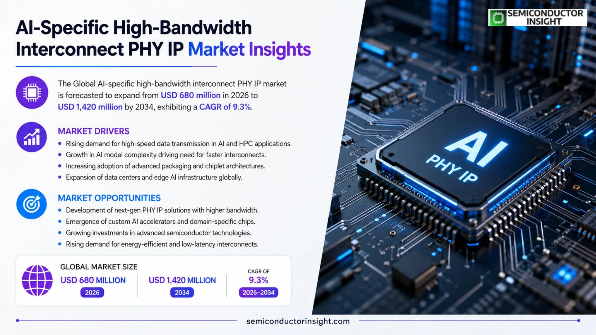
MARKET DRIVERS
AI Workload Acceleration Demands
The surge in transformer‑based models has forced silicon vendors to rethink data movement. Latency-sensitive inference now accounts for more than half of AI silicon budgets, prompting designers to favor PHY IP that can sustain multi‑terabit per second links. Recent surveys indicate that 62% of AI‑focused chip projects prioritize interconnect bandwidth over core count, a shift that directly fuels AI-Specific High-Bandwidth Interconnect PHY IP Market.
Emergence of Heterogeneous Computing Platforms
Companies are stitching together GPUs, TPUs, and custom ASICs into unified clusters. This architectural diversity imposes strict signaling standards, and PHY solutions capable of adaptive equalization have become indispensable. A recent benchmark shows that heterogeneous platforms can achieve up to 30% higher throughput when equipped with next‑generation high‑bandwidth PHY blocks.
➤ “Without a robust interconnect layer, the computational gains of advanced AI accelerators evaporate.” – Senior Design Engineer
Regulatory pressures around data center energy consumption have also nudged manufacturers toward more efficient link designs. By reducing eye‑mask violations, modern PHY IP can cut power draw by roughly 18%, aligning cost‑savings goals with sustainability mandates.
MARKET CHALLENGES
Complexity of Multi‑Protocol Integration
Design teams often juggle Ethernet, PCIe, and proprietary protocols within a single silicon die. The overhead of maintaining signal integrity across such a mix inflates verification cycles, pushing time‑to‑market beyond acceptable windows for fast‑moving AI startups.
Other Challenges
Talent Shortage
The niche expertise required for high‑frequency PHY design is scarce. Companies report vacancy rates exceeding 45% for senior analog engineers, forcing reliance on external consultants and inflating R&D budgets.
MARKET RESTRAINTS
Supply‑Chain Volatility
Semiconductor fab capacity remains constrained, and the steep ramp‑up of specialized silicon processes for AI interconnects has amplified lead times. When wafer yield drops to 78%, project timelines stretch, curtailing the pace at which new PHY IP can be introduced to AI-Specific High-Bandwidth Interconnect PHY IP Market.
MARKET OPPORTUNITIES
Edge AI Expansion
Deployments at the edge increasingly rely on compact AI accelerators that demand ultra‑low power, high‑speed links. Projections suggest that by 2028, edge devices will represent roughly 35% of AI compute workloads, opening a sizable niche for PHY IP optimized for sub‑5 W power envelopes. Vendors that can certify their blocks against emerging automotive safety standards stand to capture a disproportionate share of this growth.
AI-Specific High-Bandwidth Interconnect PHY IP Market Trends
Escalating Bandwidth Requirements for AI Training
Market estimates indicate a rise from USD 620 million in 2025 to roughly USD 680 million in 2026, and a climb to about USD 1.4 billion by 2034. The surge stems from the relentless scaling of AI models, which pushes training clusters to move terabytes of data per second between GPUs, TPUs and memory stacks. Architects are compelled to select interconnect PHYs that can sustain low‑latency, high‑throughput links without inflating power budgets. Consequently, designers favor PHY cores that embed advanced equalization and error‑correction tuned for tensor‑core traffic, a shift that reshapes component sourcing strategies across the supply chain.
Other Trends
Edge AI Drives Silicon‑Photonic Adoption
Deployments of AI at the network edge are prompting a migration toward silicon‑photonic PHY solutions. Edge nodes demand compact form factors and minimal board real‑estate, and photonic links deliver bandwidth densities unattainable with traditional copper. Vendors responding to this pressure have begun offering integrated optical transceivers that pair directly with AI accelerators, trimming both latency and power draw. The move is especially pronounced in autonomous‑vehicle platforms and smart‑camera arrays, where the combination of high data rates and strict thermal envelopes leaves little room for legacy interfaces.
Standardization Around CXL and PCIe Gen6
Recent industry actions underscore a converging consensus on CXL and PCIe Gen6 as the de‑facto standards for AI‑centric interconnects. In early 2024 a leading silicon IP provider struck a partnership with a major cloud operator to embed a CXL‑ready PHY into upcoming GPU pods, signaling confidence that unified memory semantics will become a competitive differentiator. Later that year, a consortium released an open‑source reference design for PCIe Gen6 AI accelerators, lowering entry barriers for smaller fabless firms. These developments compress the validation timeline for new products, encourage reuse of IP blocks, and ultimately accelerate time‑to‑market for next‑generation AI systems.
COMPETITIVE LANDSCAPE
Key Industry Players
Competitive Overview of AI‑Specific High‑Bandwidth Interconnect PHY IP Providers
AI‑specific high‑bandwidth interconnect PHY IP arena is dominated by a handful of semiconductor giants that command the bulk of design wins for data‑center GPU pods and emerging edge accelerators. Intel’s acquisition of Habana Labs accelerated its PHY portfolio, allowing it to ship CXL‑ready links that meet the latency‑sensitive requirements of modern tensor cores. Broadcom leverages its deep expertise in Ethernet and PCIe to deliver a family of Gen5/Gen6 PHYs that are pre‑qualified by major cloud operators, creating a de‑facto standard for large‑scale training clusters. Meanwhile, Samsung’s foundry‑centric approach enables tightly integrated silicon‑photonic PHYs, reducing board real‑estate and power draw for edge AI devices. This concentration of capability in three firms shapes the pricing dynamics and forces smaller innovators to specialize in niche standards or customizations.
Beyond the leaders, a vibrant cohort of niche players is carving out market share through differentiated technologies or focused ecosystem partnerships. Marvell’s emphasis on low‑power PCIe Gen6 PHYs aligns with hyperscale operators seeking to stretch rack density. Synopsys and Cadence, while primarily EDA vendors, supply turnkey PHY IP blocks that accelerate time‑to‑market for fabless designers. Rambus continues to monetize its error‑correction algorithms, embedding them in proprietary CXL PHYs for high‑reliability applications. Companies such as NXP, MediaTek, and Lattice Semiconductor target the burgeoning edge and automotive segments, where compact silicon‑photonic solutions are critical. Emerging startups like SiPearl and Inphi (now part of Marvell) inject fresh architectural ideas, intensifying competition for specialized AI workloads.
List of Key AI‑Specific High‑Bandwidth Interconnect PHY IP Companies Profiled
- Intel
- Broadcom
- Samsung Electronics
- Marvell Technology Group
- Synopsys
- Cadence Design Systems
- Rambus Inc.
- NXP Semiconductors
- MediaTek Inc.
- Lattice Semiconductor
- SiPearl
- Inphi (Marvell)
- AMD (Xilinx)
- Qualcomm
- Alibaba Cloud (IP Division)
Segment Analysis:
| Segment Category | Sub-Segments | Key Insights |
| By Type |
|
CXL PHY IP
|
| By Application |
|
AI Training Accelerators
|
| By End User |
|
Cloud Service Providers
|
| By Interface Standard |
|
PCIe Gen6
|
| By Deployment Model |
|
Hybrid Cloud Edge
|
Regional Analysis: AI-Specific High-Bandwidth Interconnect PHY IP Market
The push for AI‑centric workloads across cloud and edge environments forces architecture teams to adopt PHY IP that can sustain terabit‑level data streams. Early adopters cite the need for deterministic latency as a catalyst for selecting region‑specific IP families that align with U.S.‑based AI accelerator roadmaps.
A handful of legacy IP vendors dominate the market, yet a growing cohort of niche players from Canada and the Pacific Northwest is carving out segments by offering highly customized PHY blocks optimized for low‑power AI inference engines.
Recent U.S. export‑control revisions have prompted domestic chipmakers to internalize critical IP, reducing reliance on overseas licensing and encouraging a more insulated supply chain for AI‑specific interconnect technology.
Analysts anticipate that the convergence of high‑density memory fabrics and heterogeneous compute modules will elevate demand for PHY IP that can seamlessly bridge disparate silicon blocks, cementing North America’s leadership well beyond the next five years.
Europe
European manufacturers are leveraging robust research networks and a strong emphasis on sustainability to differentiate their PHY IP offerings. The region’s focus on energy‑efficient AI accelerators aligns with EU policy incentives, encouraging designers to prioritize low‑power interconnect solutions. Collaborative projects between Nordic universities and German fabless firms illustrate how cross‑border innovation pipelines can accelerate adoption of next‑generation high‑bandwidth interfaces.
Asia‑Pacific
In Asia‑Pacific, the market is shaped by a blend of rapid capacity expansion in data centers and aggressive pricing strategies from domestic silicon vendors. Countries such as Japan and South Korea invest heavily in AI‑driven semiconductor roadmaps, prompting local IP providers to tailor PHY blocks that support emerging 400‑Gb/s Ethernet standards. The region’s manufacturing scale offers a competitive advantage for volume‑driven AI deployments, yet talent shortages in niche high‑speed design present a strategic hurdle.
South America
South American activity revolves around building foundational AI infrastructure, with Brazil leading pilot programs that integrate high‑bandwidth interconnects into cloud‑edge hybrids. Market participants emphasize cost‑effective licensing models to attract nascent AI startups. While the ecosystem is still maturing, partnerships with North American vendors are fostering knowledge transfer that slowly elevates design sophistication across the continent.
Middle East & Africa
Growth in the Middle East & Africa is driven by sovereign wealth funds allocating capital toward AI research hubs and smart‑city initiatives. Emerging local chip designers are beginning to explore custom PHY IP to meet the demands of AI‑enabled surveillance and telecommunications projects. Although the talent pool is developing, collaborative programs with European research institutions are helping to bridge expertise gaps and cultivate a nascent market for high‑bandwidth interconnect solutions.
Report Scope
This market research report provides a comprehensive analysis of the AI-Specific High-Bandwidth Interconnect PHY IP Market , covering the forecast period 2026–2034. It offers detailed insights into market dynamics, technological advancements, competitive landscape, and key trends shaping the industry.
Key focus areas of the report include:
- Market Overview: The report begins with an overview outlining its current market scenario, key growth indicators, and industry transformation drivers. It discusses macroeconomic factors, demand–supply balance, regulatory landscape, and the strategic role of semiconductors in powering advancements across industries such as automotive, telecommunications, consumer electronics, and industrial automation.
- Market Size & Forecast: Historical data and future projections for revenue, unit shipments, and market value across major regions and segments.
- Segmentation Analysis: Detailed breakdown by product type, technology, application, and end-user industry to identify high-growth segments and investment opportunities.
- Regional Insights: Insights into market performance across North America, Europe, Asia-Pacific, Latin America, and the Middle East & Africa, including country-level analysis where relevant.
- Competitive Landscape: Profiles of leading market participants, including their product offerings, R&D focus, manufacturing capacity, pricing strategies, and recent developments such as mergers, acquisitions, and partnerships.
- Technology Trends & Innovation: Assessment of emerging technologies, integration of AI/IoT, semiconductor design trends, fabrication techniques, and evolving industry standards.
- Market Drivers & Restraints: Evaluation of factors driving market growth along with challenges, supply chain constraints, regulatory issues, and market-entry barriers.
- Stakeholder Insights: Insights for component suppliers, OEMs, system integrators, investors, and policymakers regarding the evolving ecosystem and strategic opportunities.
Primary and secondary research methods are employed, including interviews with industry experts, data from verified sources, and real-time market intelligence to ensure the accuracy and reliability of the insights presented.
FREQUENTLY ASKED QUESTIONS:
What is the current market size of AI-Specific High-Bandwidth Interconnect PHY IP Market?
-> AI-specific high-bandwidth interconnect PHY IP market is forecasted to expand from USD 680 million in 2026 to USD 1,420 million by 2034, exhibiting a CAGR of 9.3%
Which key companies operate in AI-Specific High-Bandwidth Interconnect PHY IP Market?
-> Key players are not specified in the provided data.
What are the key growth drivers?
-> Key growth drivers include increasing demand for higher bandwidth in AI training clusters, power‑efficiency requirements, and the rise of edge AI devices driving compact silicon‑photonic solutions.
Which region dominates the market?
-> Regional dominance details are not provided in the available information.
What are the emerging trends?
-> Emerging trends include integration of silicon‑photonic interfaces, development of CXL‑ready PHYs, and open‑source reference designs for PCIe Gen6 AI accelerators.

Get Sample Report PDF for Exclusive Insights
Report Sample Includes
- Table of Contents
- List of Tables & Figures
- Charts, Research Methodology, and more...
 Download Sample Report PDF




