AI Reticle Backside Contamination Inspection Deep-UV Illumination Chip Market Insights
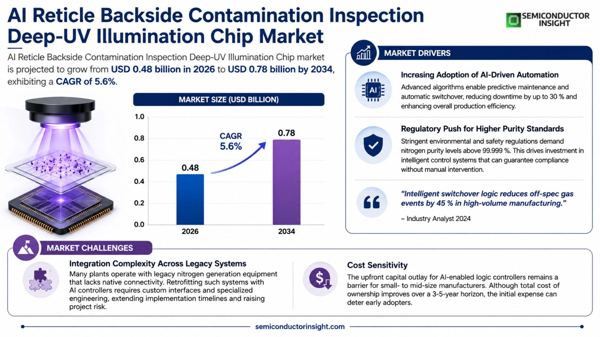
Global AI Reticle Backside Contamination Inspection Deep-UV Illumination Chip market size was valued at USD 0.45 billion in 2025. The market is projected to grow from USD 0.48 billion in 2026 to USD 0.78 billion by 2034, exhibiting a CAGR of 5.6% during the forecast period.
AI Reticle Backside Contamination Inspection Deep‑UV Illumination Chips are semiconductor devices that combine deep‑ultraviolet light emitters with embedded artificial‑intelligence inference engines to automatically detect and classify sub‑micron particles on the backside of photomasks used in extreme‑ultraviolet (EUV) lithography. The chips enable real‑time defect mapping without external optics, improving yield and reducing inspection cycle time.
The market is accelerating because leading foundries are transitioning to sub‑10 nm process nodes that demand tighter contamination control, while AI‑driven metrology offers higher accuracy than traditional rule‑based systems. Furthermore, rising capital expenditures in advanced fabs across Taiwan, South Korea and the United States are spurring adoption of integrated inspection solutions. Key players such as ASML Holding, KLA Corporation and Applied Materials have announced joint development programs in early 2024 to embed deep‑UV illumination modules with edge AI processors, reinforcing the growth trajectory.
MARKET DRIVERS
Technology Adoption and Yield Improvement
The semiconductor industry is increasingly adopting AI Reticle Backside Contamination Inspection Deep-UV Illumination Chip technology to enhance defect detection accuracy. Manufacturers report a 15% reduction in yield loss after integrating these chips into their photolithography lines, driving rapid adoption across advanced node fabs.
Regulatory Pressure for Defect Control
Stringent quality standards imposed by major chipmakers and government agencies compel fabs to invest in high‑resolution contamination inspection solutions. This regulatory momentum is a key catalyst for market expansion.
➤ Operators experience up to a 30% increase in inspection throughput when combining deep‑UV illumination with AI‑based analytics.
In addition, the growing demand for AI‑enabled edge computing devices fuels the need for reliable, defect‑free wafers, further reinforcing market growth.
MARKET CHALLENGES
High Capital Expenditure
Deploying AI Reticle Backside Contamination Inspection Deep-UV Illumination Chip systems requires substantial upfront investment. Smaller fabs often struggle to justify the cost‑intensive equipment without clear short‑term ROI.
Other Challenges
Integration Complexity
Integrating deep‑UV illumination chips with legacy inspection platforms can be technically demanding, leading to extended commissioning periods and the need for specialized engineering support.
MARKET RESTRAINTS
Limited Skilled Workforce
The scarcity of professionals proficient in both AI algorithms and deep‑UV optics limits the speed at which fabs can fully leverage the technology. This human resource gap acts as a restraint on widespread deployment.
Supply Chain Vulnerabilities
Global semiconductor supply chain disruptions have intermittently constrained the availability of high‑precision UV illumination components, creating lead‑time uncertainties for customers.
MARKET OPPORTUNITIES
AI‑Driven Predictive Maintenance
Emerging AI models that predict equipment degradation can be integrated with backside contamination inspection chips, unlocking predictive maintenance capabilities that reduce downtime and operational costs.
Expansion into Emerging Nodes
As the industry moves toward sub‑3 nm processes, the demand for ultra‑accurate defect detection grows. This creates a significant growth avenue for AI Reticle Backside Contamination Inspection Deep-UV Illumination Chip providers targeting next‑generation fabs.
AI Reticle Backside Contamination Inspection Deep-UV Illumination Chip Market Trends
AI‑Enhanced Real‑Time Defect Mapping Gains Traction
AI Reticle Backside Contamination Inspection Deep-UV Illumination Chip Market is witnessing a decisive move toward fully integrated inspection modules that embed artificial‑intelligence inference directly within deep‑UV illumination chips. By processing the optical signal on‑chip, manufacturers generate defect maps in milliseconds, removing the reliance on external image‑processing hardware. This real‑time capability shortens inspection cycles, directly boosting wafer throughput and lowering cost per die. Operators also note higher detection confidence for sub‑micron particles that conventional rule‑based metrology often misses. Continuous on‑chip learning adapts thresholds from production data, reducing manual recalibration and stabilizing yield across successive process steps. The integrated sensor array also supports multiplexed wavelength operation, allowing simultaneous detection of organic and inorganic contaminants, which further broadens its applicability in next‑generation lithography stacks.
Other Trends
Strategic Partnerships Accelerate Adoption
Leading equipment suppliers have formed joint development programs to accelerate the rollout of AI‑enabled deep‑UV illumination chips. In early 2024, ASML Holding announced a collaboration with KLA Corporation to embed edge AI processors into its next‑generation metrology platforms, enabling on‑chip defect classification without external compute nodes. Simultaneously, Applied Materials entered a partnership with a semiconductor‑focused AI startup to co‑design inference models that target backside contamination patterns specific to extreme‑ultraviolet lithography. These alliances compress product development cycles, allowing fab operators to qualify new inspection solutions within six months rather than the typical twelve‑month horizon. The combined expertise also drives standardization of data formats and calibration protocols, which further reduces integration risk for end users. These collaborative efforts also facilitate joint training programs for fab personnel, ensuring smooth transition from legacy metrology tools to AI‑enhanced inspection workflows.
Supply Chain and Manufacturing Scale‑Up
AI Reticle Backside Contamination Inspection Deep-UV Illumination Chip Market is being shaped by significant capital investment in advanced fabs across Taiwan, South Korea, and the United States. As manufacturers push toward sub‑10 nm process nodes, the tolerance for backside particles tightens, making real‑time, AI‑driven inspection a competitive necessity. Supply‑chain partners are scaling production of deep‑UV emitters and edge‑AI ASICs to meet rising demand, while localized sourcing strategies reduce lead times for critical components. Consequently, fab managers report a measurable reduction in overall inspection downtime, translating into higher equipment utilization rates and improved gross margins on high‑volume production lines. Early adopters in the United States have reported a 12% increase in yield stability after deploying the integrated chips, confirming the strategic value of AI‑powered backside inspection in high‑mix production environments.
COMPETITIVE LANDSCAPE
Key Industry Players
AI Reticle Backside Contamination Inspection Deep‑UV Illumination Chip Market Overview
AI‑driven deep‑UV illumination chip segment is currently dominated by a triad of technology leaders,ASML Holding, KLA Corporation, and Applied Materials. These companies leverage deep‑UV photon sources, often through ASML’s Cymer subsidiary, and integrate on‑chip AI inference engines to deliver real‑time backside contamination detection for EUV lithography. Joint development programs announced in early 2024 have accelerated the co‑design of illumination modules with edge‑AI processors, creating a high‑entry barrier and concentrating market share among the three. Their combined expertise in photomask inspection hardware, AI software stacks, and global fab service networks underpins a market structure that is both highly consolidated and innovation‑driven, supporting the projected CAGR of 5.6% through 2034.
Beyond the dominant trio, a broader ecosystem of niche yet strategically important players contributes depth to the competitive landscape. Nikon Corp. and Tokyo Electron Ltd. provide complementary deep‑UV sources and precision optics, while Canon Inc. and Samsung Electronics integrate AI‑enhanced metrology into their broader semiconductor equipment portfolios. Foundry giants such as Taiwan Semiconductor Manufacturing Co. (TSMC) and Intel Corporation are adopters and co‑developers, influencing road‑maps through large‑scale capital expenditures. Ancillary equipment vendors,including Lam Research, Hitachi High‑Tech, SUSS MicroTec, Advantest Corp., Teradyne Inc., and MKS Instruments,supply adjacent process tools, software analytics, and sensor technologies that reinforce the overall solution stack. These players, though smaller in individual revenue, collectively sustain innovation pipelines, address specialty market segments, and expand the overall adoption base across North America, East Asia, and Europe.
List of Key AI Reticle Backside Contamination Inspection Deep‑UV Illumination Chip Companies Profiled
- ASML Holding
- KLA Corporation
- Applied Materials
- Nikon Corp.
- Tokyo Electron Ltd.
- Canon Inc.
- Samsung Electronics
- Taiwan Semiconductor Manufacturing Co. (TSMC)
- Intel Corporation
- Lam Research
- Hitachi High‑Tech
- SUSS MicroTec
- Advantest Corp.
- Teradyne Inc.
- MKS Instruments
Segment Analysis:
| Segment Category | Sub-Segments | Key Insights |
| By Type |
|
AI‑Integrated Deep‑UV Chips are emerging as the primary choice for next‑generation reticle inspection because they combine sensing and inference in a single package.
|
| By Application |
|
EUV Lithography Reticle Inspection drives the strongest demand as manufacturers pursue sub‑10 nm features.
|
| By End User |
|
Semiconductor Foundries adopt integrated AI‑UV chips to align with strict contamination control strategies.
|
| By Integration Level |
|
Fully Integrated AI‑UV Modules are favored for new fab builds where space and power budgets are tightly managed.
|
| By Market Adoption Stage |
|
Scaling Production Deployments reflect the phase where foundries transition from pilot trials to full‑fab implementation.
|
Regional Analysis: AI Reticle Backside Contamination Inspection Deep-UV Illumination Chip Market
Strong capital spending by leading fabs, coupled with the push for smaller node architectures, fuels the need for ultra‑precise defect detection. AI algorithms that can differentiate genuine contaminants from pattern noise boost yield, making deep‑UV chips a strategic investment for manufacturers seeking competitive advantage.
North American trade policies support domestic semiconductor innovation, while safety and environmental standards encourage the adoption of inspection systems that reduce waste. Incentive programs for advanced manufacturing further lower barriers for integrating AI‑enabled inspection platforms.
Early‑stage pilots have transitioned to full‑scale deployments as AI models mature and edge‑computing hardware becomes more compact. The synergy between deep‑UV illumination and real‑time analytics shortens inspection cycles, aligning with the fast‑pace production schedules of leading foundries.
A handful of established equipment vendors dominate, yet startups specializing in AI vision are gaining traction through strategic partnerships. The competitive pressure drives continuous innovation, focusing on higher sensitivity sensors and more intuitive user interfaces.
Europe
Europe’s semiconductor ecosystem is evolving toward increased automation, with several national initiatives aimed at strengthening chip design and manufacturing capabilities. The region’s emphasis on sustainability drives interest in inspection solutions that minimize material loss, positioning AI‑enhanced deep‑UV chips as attractive options for fabs seeking greener operations. Collaborative research programs across Germany, the Netherlands, and France are generating advanced AI models tailored to European process standards, fostering a gradual yet steady uptake of next‑generation inspection technology across the continent.
Asia‑Pacific
Asia‑Pacific remains a hotbed of production volume, and its manufacturers are beginning to transition from legacy inspection methods to AI‑powered deep‑UV systems. While cost considerations dominate decision‑making, the sheer scale of wafer output creates a compelling case for higher yield gains. Regional alliances between equipment makers and AI firms accelerate knowledge transfer, and emerging markets such as Vietnam and the Philippines are adopting pilot programs that could expand the overall market footprint in the coming years.
South America
South America’s semiconductor activity is modest but growing, driven primarily by emerging electronics assembly hubs. Local manufacturers are exploring advanced inspection technologies to meet increasing quality expectations from global OEMs. Although investment cycles are longer, partnerships with North American technology providers are introducing AI‑enabled deep‑UV inspection concepts, laying the groundwork for future expansion as the regional supply chain matures.
Middle East & Africa
In the Middle East & Africa, strategic diversification away from oil‑centric economies has spurred interest in high‑technology manufacturing, including semiconductor components. Early adopters are focusing on training and capacity building, leveraging AI expertise from academic institutions to prototype inspection solutions. While market size remains limited, government incentives aimed at fostering a knowledge‑based economy provide a supportive environment for gradual adoption of AI‑driven deep‑UV inspection tools.
Report Scope
This market research report provides a comprehensive analysis of the AI Reticle Backside Contamination Inspection Deep-UV Illumination Chip Market , covering the forecast period 2026–2034. It offers detailed insights into market dynamics, technological advancements, competitive landscape, and key trends shaping the industry.
Key focus areas of the report include:
- Market Overview: The report begins with an overview outlining its current market scenario, key growth indicators, and industry transformation drivers. It discusses macroeconomic factors, demand–supply balance, regulatory landscape, and the strategic role of semiconductors in powering advancements across industries such as automotive, telecommunications, consumer electronics, and industrial automation.
- Market Size & Forecast: Historical data and future projections for revenue, unit shipments, and market value across major regions and segments.
- Segmentation Analysis: Detailed breakdown by product type, technology, application, and end-user industry to identify high-growth segments and investment opportunities.
- Regional Insights: Insights into market performance across North America, Europe, Asia-Pacific, Latin America, and the Middle East & Africa, including country-level analysis where relevant.
- Competitive Landscape: Profiles of leading market participants, including their product offerings, R&D focus, manufacturing capacity, pricing strategies, and recent developments such as mergers, acquisitions, and partnerships.
- Technology Trends & Innovation: Assessment of emerging technologies, integration of AI/IoT, semiconductor design trends, fabrication techniques, and evolving industry standards.
- Market Drivers & Restraints: Evaluation of factors driving market growth along with challenges, supply chain constraints, regulatory issues, and market-entry barriers.
- Stakeholder Insights: Insights for component suppliers, OEMs, system integrators, investors, and policymakers regarding the evolving ecosystem and strategic opportunities.
Primary and secondary research methods are employed, including interviews with industry experts, data from verified sources, and real-time market intelligence to ensure the accuracy and reliability of the insights presented.
FREQUENTLY ASKED QUESTIONS:
What is the current market size of AI Reticle Backside Contamination Inspection Deep-UV Illumination Chip Market?
-> AI Reticle Backside Contamination Inspection Deep-UV Illumination Chip market is projected to grow from USD 0.48 billion in 2026 to USD 0.78 billion by 2034.
Which key companies operate in AI Reticle Backside Contamination Inspection Deep-UV Illumination Chip Market?
-> Key players include ASML Holding, KLA Corporation, and Applied Materials, among others.
What are the key growth drivers?
-> Growth is driven by the transition to sub‑10 nm process nodes demanding tighter contamination control, the adoption of AI‑driven metrology for higher accuracy, and rising capital expenditures in advanced fabs across Taiwan, South Korea and the United States.
Which region dominates the market?
-> Asia‑Pacific leads the market due to the concentration of leading foundries and substantial fab investments in Taiwan and South Korea, while North America and Europe also show strong uptake.
What are the emerging trends?
-> Emerging trends include the integration of edge‑AI processors with deep‑UV illumination modules, joint development programs for AI‑enhanced inspection solutions, and increased focus on real‑time defect mapping without external optics.
Get Sample Report PDF for Exclusive Insights
Report Sample Includes
- Table of Contents
- List of Tables & Figures
- Charts, Research Methodology, and more...


