
AI Processor Die-to-Die Interface IP Market Insights
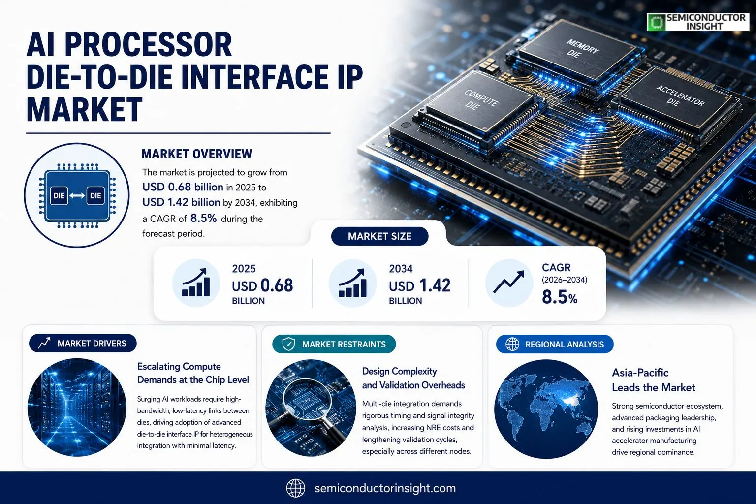
AI Processor Die-to-Die Interface IP market size was valued at USD 0.68 billion in 2025. Forecast indicates growth from USD 0.68 billion in 2025 to USD 1.42 billion by 2034, exhibiting a CAGR of 8.5 % during the forecast period.
AI Processor Die-to-Die Interface IP comprises licensed intellectual property that enables high‑bandwidth, low‑latency communication between separate silicon dies within an AI accelerator package. The technology supports heterogeneous integration of compute cores, memory stacks and specialized accelerators, allowing designers to overcome interconnect bottlenecks while maintaining power efficiency.The market gains momentum because semiconductor manufacturers are consolidating multiple dies into single packages to meet exploding AI workload demands.Furthermore, rising adoption of advanced packaging such as chip‑on‑wafer‑on‑substrate (CoWoS) and fan‑out wafer‑level packaging (FOWLP) fuels demand for robust die‑to‑die interfaces.In March 2024, Arm announced a strategic licensing agreement with TSMC that expands access to its latest interface specifications for next‑generation AI processors, underscoring industry confidence in this segment.
MARKET DRIVERS
Escalating Compute Demands at the Chip Level
The surge in AI inference workloads on edge devices forces silicon designers to locate memory, accelerators, and sensors within a single package. Die‑to‑die interfaces that can move terabytes per second become the logical solution, prompting semiconductor vendors to embed dedicated IP blocks that bridge multiple dies with minimal latency. This architectural shift fuels the expansion of AI Processor Die-to-Die Interface IP Market.
Standardization of High‑Speed Protocols
Industry consortia such as JEDEC and OCP have converged on unified signaling standards, reducing integration risk for chipmakers. The clarity around electrical and mechanical specifications accelerates time‑to‑market for new products, making IP licensing an attractive shortcut for firms lacking in‑house expertise.
➤ “Companies that secure a proven die‑to‑die IP suite today will avoid costly redesign cycles as AI workloads continue to scale.”
Overall, the combination of workload pressure, protocol harmonization, and the need for rapid product roll‑outs creates a fertile environment for vendors offering AI Processor Die-to-Die Interface IP solutions.
MARKET CHALLENGES
Design Complexity and Validation Overheads
Integrating multiple dies demands meticulous timing closure and signal‑integrity analysis. Since each die may be fabricated on a different process node, validation cycles lengthen, raising NRE costs for customers. Insufficient verification tools exacerbate the risk of late‑stage redesigns, deterring smaller players from adopting advanced interfaces.
Other Challenges
Supply Chain Visibility
The fragmented nature of semiconductor foundry contracts means that lead times for compatible dies are unpredictable. When a critical die is delayed, the entire die‑to‑die interface schedule stalls, pressuring OEMs to maintain higher safety stocks, which in turn inflates overall system cost.
MARKET RESTRAINTS
Cost Sensitivity in High‑Volume Segments
Mass‑market devices such as smartphones and entry‑level IoT nodes operate on razor‑thin margins. The incremental licensing fee for AI Processor Die-to-Die Interface IP can represent a disproportionate expense, leading manufacturers to postpone adoption until economies of scale drive the unit cost down.
MARKET OPPORTUNITIES
Emergence of Multi‑AI Accelerator Platforms
Next‑generation data‑center servers are beginning to incorporate clusters of heterogeneous AI accelerators across stacked dies. This architecture opens a sizable revenue channel for IP providers that can deliver low‑power, high‑throughput die‑to‑die bridges optimized for mixed‑precision workloads. Early movers stand to capture a sizeable share of the evolving AI Processor Die-to-Die Interface IP Market.
AI Processor Die-to-Die Interface IP Market Trends
Consolidation of Heterogeneous Dies Fuels Interface Demand
The shift toward integrating compute cores, high‑bandwidth memory stacks and specialty accelerators inside a single package has reshaped design priorities. By eliminating the need for a monolithic die, manufacturers can tailor each component to its optimal process node, yet they must still achieve sub‑nanosecond signaling across the physical gap. Die‑to‑die interface IP supplies the necessary protocol and physical‑layer robustness, allowing the overall system to sustain AI workloads that would otherwise be throttled by interconnect latency. This architectural move is not merely a technical curiosity; it directly addresses the power‑budget constraints that dominate data‑center and edge deployments, enabling higher performance per watt while preserving silicon yield advantages.
Other Trends
Advanced Packaging Adoption
Technologies such as chip‑on‑wafer‑on‑substrate (CoWoS) and fan‑out wafer‑level packaging (FOWLP) have graduated from niche to mainstream within the last two years. Their ability to expose large interconnect pitches and embed multiple dies in a thin form factor makes them natural partners for high‑speed interface IP. As equipment suppliers streamline the manufacturing flow, the time‑to‑market for new AI accelerator modules shortens, prompting design teams to rely on proven interface specifications rather than bespoke solutions. This convergence reduces engineering risk and aligns the supply chain around a common set of validation criteria, which in turn accelerates adoption across a broader customer base.
Strategic Licensing Moves
In early 2024, a leading architecture licensor secured a multi‑year agreement with a major foundry to broaden access to its latest die‑to‑die specifications. The deal emphasizes cross‑company collaboration, ensuring that emerging AI processors can tap into a vetted IP ecosystem without reinventing the communication stack. For end‑users, the licensing model translates into faster design iterations and a clearer path to compliance with power‑efficiency standards. As more players enter the ecosystem, AI Processor Die-to-Die Interface IP Market is poised to mature into a platform where differentiated performance originates from algorithmic innovation rather than interconnect engineering.
COMPETITIVE LANDSCAPE
Key Industry Players
AI Processor Die‑to‑Die Interface IP – Competitive Overview
The AI processor die‑to‑die interface segment is anchored by a handful of licensors whose architectures have become de‑facto standards for high‑performance AI accelerators. Arm leads the field, leveraging its recent licensing pact with TSMC to extend the latest CoWoS‑compatible interface specifications across multiple foundry partners. This move not only secures Arm’s dominance in the IP layer but also pressures rivals to align their roadmaps with the same bandwidth targets, reinforcing a top‑down market structure where a few IP custodians dictate design conventions. Intel’s acquisition of specialized interconnect assets and its own in‑house interface suite further narrows the competitive set, as the company integrates the IP directly into its Xe‑HPC and Ponte Vecchio families, creating a vertically integrated offering that blends silicon and IP under one roof.Beyond the marquee names, a constellation of niche players contributes depth and differentiation. Samsung Electronics supplies proprietary high‑density TSV‑based interconnects optimized for its memory‑centric AI modules, while Foundries and TSMC provide foundry‑specific extensions that tailor latency and power envelopes for chiplet ecosystems. Synopsys and Cadence monetize their DesignWare and IP‑Lite portfolios, respectively, delivering configurable PHY blocks that appeal to fabless designers seeking quick time‑to‑market. Rambus, Marvell, and Qualcomm each market specialized high‑speed link IP that addresses distinct segments such as automotive AI and edge inference, reinforcing the market’s fragmented yet collaborative character.
List of Key AI Processor Die‑to‑Die Interface IP Companies Profiled
- Arm Limited
- TSMC
- Intel Corporation
- Advanced Micro Devices (AMD)
- NVIDIA Corporation
- Samsung Electronics
- Foundries
- Synopsys, Inc.
- Cadence Design Systems, Inc.
- Rambus Inc.
- Marvell Technology Group Ltd.
- Qualcomm Incorporated
- Imagination Technologies Ltd.
- Broadcom Inc.
- Skywater Technology Foundry
Segment Analysis:
| Segment Category | Sub-Segments | Key Insights |
| By Type |
|
High‑Bandwidth Serial Interface
|
| By Application |
|
Data‑Center AI Accelerators
|
| By End User |
|
Cloud Service Providers
|
| By Architecture |
|
Tensor Processing Units (TPUs)
|
| By Packaging |
|
CoWoS
|
Regional Analysis: AI Processor Die-to-Die Interface IP Market
North America
Collaborative platforms linking EDA toolmakers, IP specialists, and chip architects have matured, allowing rapid co‑development of custom interconnect blocks. The ecosystem’s openness reduces time‑to‑market for niche AI accelerators that depend on precise die‑to‑die signaling.
Recent disruptions prompted manufacturers to diversify fab capacity across the United States and Canada, embedding redundancy into the production of high‑performance interface IP. This strategy mitigates exposure to single‑source bottlenecks.
A proactive stance by the Federal Trade Commission on IP enforcement and export controls ensures a predictable environment for cross‑border licensing, encouraging multinational consortia to pool R&D resources.
Universities in the region have introduced dedicated curricula on heterogeneous integration, feeding a steady stream of engineers proficient in both logic design and advanced packaginga critical advantage for AI Processor Die-to-Die Interface IP Market.
Europe
European manufacturers focus on energy‑efficient interconnect schemes, reflecting the bloc’s stringent sustainability policies. Design houses are embedding low‑power signaling techniques into their IP suites, targeting data‑center operators that prioritize carbon footprints. Collaboration between German fab providers and French IP developers yields solutions that balance throughput with power budgets, a combination increasingly demanded by enterprise AI workloads. The regulatory environment, shaped by the European Union’s digital strategy, encourages standard‑based licensing, which lowers integration risk for system integrators across the continent.
Asia‑Pacific
The Asia‑Pacific region leverages its scale of production to experiment with novel die‑to‑die bonding methods, often coupling domestic fab capacity with aggressive pricing models. While cost considerations dominate, customers also seek performance parity with Western peers, driving a surge in joint ventures that blend Asian manufacturing efficiency with imported design expertise. Government incentives aimed at advancing semiconductor sovereignty have spurred investment in domestic IP cores, enabling the region to transition from volume‑only suppliers to creators of differentiated interface technology.
South America
In South America, adoption is still in its infancy, but niche players are targeting automotive AI applications where rugged, high‑bandwidth connections are essential. Local design firms partner with North American IP vendors to import proven interface blocks, customizing them for tropical operating conditions. The gradual rollout of 5G infrastructure creates ancillary demand for edge‑located AI processors, providing a modest but growing market for specialized die‑to‑die solutions.
Middle East & Africa
The Middle East & Africa region is exploring AI‑enabled edge analytics for oil‑field monitoring and smart‑city initiatives. Limited local fab capability means most interface IP is sourced through licensing agreements with established providers. Regional investment funds are beginning to back startups that focus on low‑latency interconnects tailored for remote sensing, indicating an emerging niche that could attract further international collaboration.
Report Scope
This market research report provides a comprehensive analysis of the AI Processor Die-to-Die Interface IP Market , covering the forecast period 2026–2034. It offers detailed insights into market dynamics, technological advancements, competitive landscape, and key trends shaping the industry.
Key focus areas of the report include:
- Market Overview: The report begins with an overview outlining its current market scenario, key growth indicators, and industry transformation drivers. It discusses macroeconomic factors, demand–supply balance, regulatory landscape, and the strategic role of semiconductors in powering advancements across industries such as automotive, telecommunications, consumer electronics, and industrial automation.
- Market Size & Forecast: Historical data and future projections for revenue, unit shipments, and market value across major regions and segments.
- Segmentation Analysis: Detailed breakdown by product type, technology, application, and end-user industry to identify high-growth segments and investment opportunities.
- Regional Insights: Insights into market performance across North America, Europe, Asia-Pacific, Latin America, and the Middle East & Africa, including country-level analysis where relevant.
- Competitive Landscape: Profiles of leading market participants, including their product offerings, R&D focus, manufacturing capacity, pricing strategies, and recent developments such as mergers, acquisitions, and partnerships.
- Technology Trends & Innovation: Assessment of emerging technologies, integration of AI/IoT, semiconductor design trends, fabrication techniques, and evolving industry standards.
- Market Drivers & Restraints: Evaluation of factors driving market growth along with challenges, supply chain constraints, regulatory issues, and market-entry barriers.
- Stakeholder Insights: Insights for component suppliers, OEMs, system integrators, investors, and policymakers regarding the evolving ecosystem and strategic opportunities.
Primary and secondary research methods are employed, including interviews with industry experts, data from verified sources, and real-time market intelligence to ensure the accuracy and reliability of the insights presented.
FREQUENTLY ASKED QUESTIONS:
What is the current market size of AI Processor Die-to-Die Interface IP Market?
-> AI Processor Die-to-Die Interface IP Market was valued at USD 0.68 billion in 2025 and is expected to reach USD 1.42 billion by 2034, exhibiting a CAGR of 8.5 % during the forecast period.
Which key companies operate in AI Processor Die-to-Die Interface IP Market?
-> Key players include Arm, TSMC, Nvidia, Intel, AMD, and Samsung, among others.
What are the key growth drivers?
-> Key growth drivers include consolidation of multiple dies into single packages, rising adoption of advanced packaging technologies such as CoWoS and FOWLP, and accelerating AI workload demands across data centers and edge devices.
Which region dominates the market?
-> Asia-Pacific leads the market, driven by the presence of major semiconductor fabs and strong investments in advanced packaging infrastructure.
What are the emerging trends?
-> Emerging trends include heterogeneous integration of compute, memory and accelerator dies, increased licensing agreements for next‑generation interface specifications, and the development of low‑latency, high‑bandwidth die‑to‑die IP blocks to support AI accelerator scaling.
Get Sample Report PDF for Exclusive Insights
Report Sample Includes
- Table of Contents
- List of Tables & Figures
- Charts, Research Methodology, and more...
 Download Sample Report PDF






