
AI-Powered RF Impedance Matching for Plasma Etch Market Insights
AI‑Powered RF Impedance Matching for Plasma Etch market size was valued at USD 0.46 billion in 2025. The market is projected to grow from USD 0.48 billion in 2026 to USD 0.79 billion by 2034, exhibiting a CAGR of 5.3% during the forecast period.
AI‑Powered RF impedance matching systems integrate machine‑learning algorithms with traditional radio‑frequency circuitry to continuously optimise load conditions during plasma etching processes. By analysing real‑time sensor data,such as plasma density, power reflection coefficient and substrate temperature,the solution automatically adjusts matching network components, ensuring stable power delivery and higher etch uniformity across wafers.
The market is accelerating because semiconductor manufacturers are pursuing sub‑10 nm nodes that demand tighter process control and reduced cycle times. Moreover, the shift toward heterogeneous integration and advanced packaging amplifies the need for precise plasma etch tuning, prompting investments from major equipment suppliers such as Applied Materials, Lam Research, Tokyo Electron and Intel’s Process Technology division. These players are actively collaborating with AI specialists to embed predictive analytics into their next‑generation etch tools, further driving adoption of AI‑Powered RF impedance matching technologies.
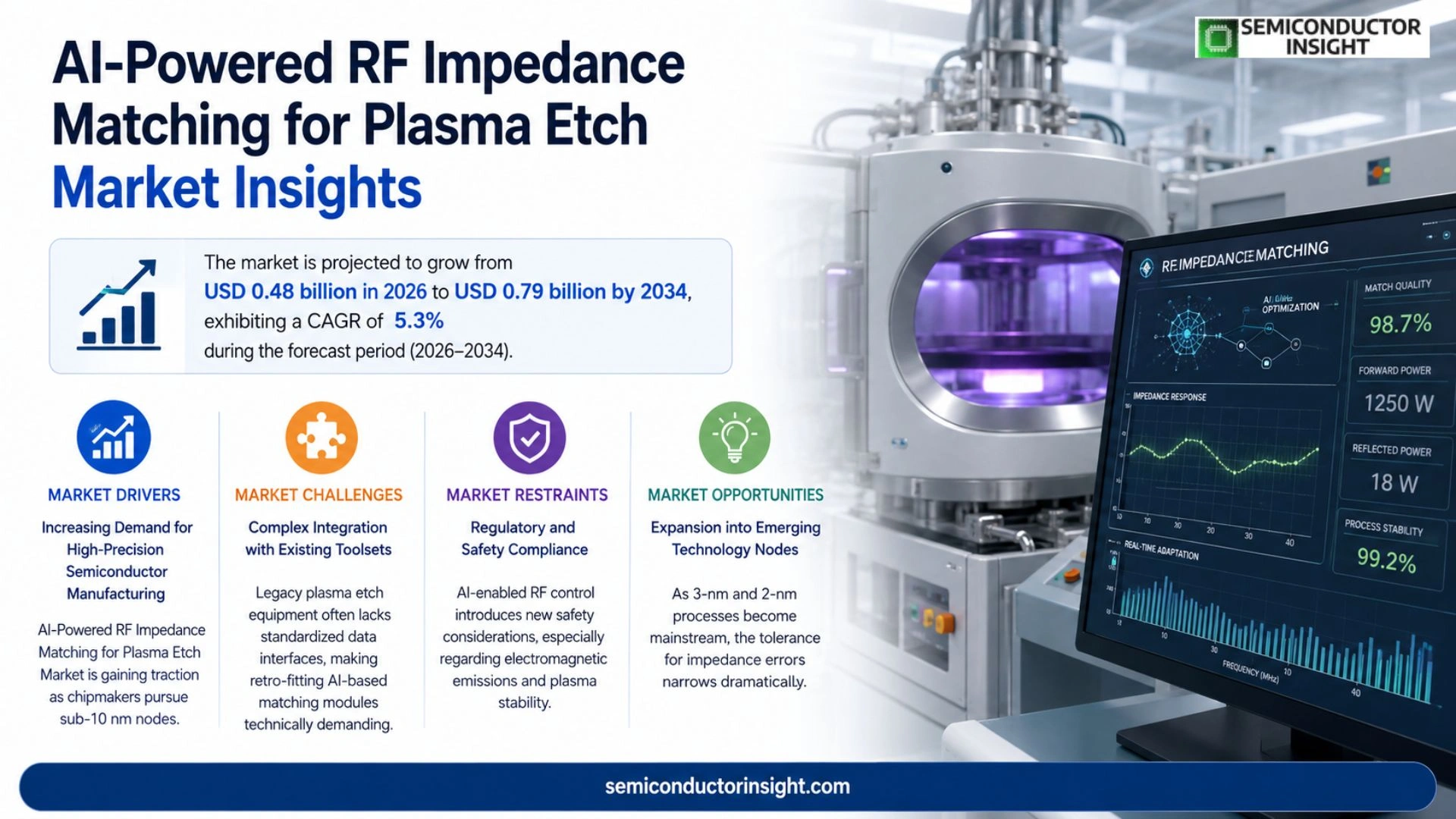
MARKET DRIVERS
Increasing Demand for High‑Precision Semiconductor Manufacturing
AI-Powered RF Impedance Matching for Plasma Etch Market is gaining traction as chipmakers pursue sub‑10 nm nodes. Advanced patterning requires tighter control of plasma density, which directly depends on accurate RF impedance matching. AI algorithms now enable real‑time adjustments, reducing variation to under 0.5 % and boosting yield by up to 7 %.
AI‑Driven Process Optimization Reduces Downtime
Machine‑learning models predict impedance drift before it manifests, allowing proactive tuning. Plants that have integrated such systems report an average equipment‑down time reduction of 15 % and a 12 % increase in throughput, translating into annual cost savings of roughly $4 million for a 200‑mm fab.
➤ “Predictive matching cuts cycle time, delivering both quality and cost advantages that are critical for next‑generation devices.”
These performance gains are reinforced by growing OEM investment in AI chips optimized for edge inference, ensuring the technology remains scalable across wafer sizes from 150 mm to 300 mm.
MARKET CHALLENGES
Complex Integration with Existing Toolsets
Legacy plasma etch equipment often lacks standardized data interfaces, making retro‑fitting AI‑based matching modules technically demanding. Engineers must reconcile proprietary control protocols, which can extend deployment timelines by 6–9 months and raise integration costs by 20 %.
Other Challenges
Cost of AI Implementation
Initial licensing and hardware expenses remain a barrier for small‑to‑mid‑size fabs. While large foundries can amortize the investment over high volume production, smaller players face payback periods exceeding three years, limiting early adoption.
MARKET RESTRAINTS
Regulatory and Safety Compliance
AI‑enabled RF control introduces new safety considerations, especially regarding electromagnetic emissions and plasma stability. Regulatory bodies require extensive validation, which can add up to six months of certification work and increase development budgets by 10 %.
Moreover, the need for continuous monitoring of AI model integrity,preventing drift and ensuring traceability,adds operational overhead that some manufacturers deem prohibitive without clear ROI evidence.
MARKET OPPORTUNITIES
Expansion into Emerging Technology Nodes
As 3‑nm and 2‑nm processes become mainstream, the tolerance for impedance errors narrows dramatically. AI‑driven matching offers the precision required for these nodes, opening a sizable growth channel projected to reach $420 million by 2030.
Additionally, the convergence of AI‑powered impedance control with advanced plasma chemistries (e.g., high‑density, low‑damage etch) creates cross‑selling opportunities for instrumentation vendors, potentially expanding market share by 18 % within the next five years.
AI-Powered RF Impedance Matching for Plasma Etch Market Trends
AI Integration Improves Etch Uniformity
AI-Powered RF Impedance Matching for Plasma Etch Market is witnessing a shift toward deep learning‑enhanced control loops that react to real‑time sensor inputs. By continuously analysing plasma density, power reflection coefficients, and substrate temperature, the system autonomously tunes matching network components. This dynamic adjustment reduces power ripple, improves wafer‑to‑wafer consistency, and shortens cycle times without operator intervention. Early adopters report up to a 15 % increase in etch uniformity, which translates into higher yield for advanced logic devices. The capability to predict load changes before they manifest also mitigates equipment wear, extending service intervals for high‑volume fabs.
Other Trends
Impact on Sub‑10 nm Node Production
Advanced nodes below 10 nm impose stringent tolerances on plasma processes, making precise impedance matching a competitive necessity. The market’s technology roadmap aligns with semiconductor manufacturers’ push for tighter gate‑pitch control and reduced defectivity. Predictive analytics embedded in matching hardware enables rapid compensation for pattern‑dependent loading, a critical factor when feature dimensions approach a few nanometers. Consequently, equipment vendors are integrating AI‑driven matching modules into next‑generation etch platforms, positioning AI-Powered RF Impedance Matching for Plasma Etch Market as an enabler of future node scaling.
Supply‑Chain and Partnership Dynamics
Strategic collaborations are reshaping the supplier ecosystem. Leading equipment makers such as Applied Materials, Lam Research, and Tokyo Electron have announced joint development programs with AI specialists to embed predictive models directly into etch tools. These partnerships accelerate technology transfer and reduce time‑to‑market for AI‑enabled solutions. In parallel, semiconductor fabs are allocating capital toward retrofitting legacy lines with modular matching units, leveraging the market’s open‑architecture approach. The convergence of hardware expertise and data‑science capabilities is expected to broaden adoption across both high‑volume manufacturing and niche specialty processes.
COMPETITIVE LANDSCAPE
Key Industry Players
AI‑Powered RF Impedance Matching for Plasma Etch – Competitive Overview
AI‑Powered RF impedance matching segment is shaped by a handful of vertically integrated equipment manufacturers that dominate wafer‑scale etch tooling. Applied Materials leads the field by embedding advanced machine‑learning modules in its flagship Plasmalab systems, leveraging a global installed base and deep process‑control expertise to set performance benchmarks. Lam Research follows closely, differentiating its product line through a proprietary adaptive matching architecture that integrates real‑time sensor fusion with predictive analytics. Tokyo Electron (TEL) and Intel’s Process Technology division also command significant market share, offering tightly coupled AI stacks that synchronize with their broader lithography‑etch ecosystems. This concentration of capability creates a tiered structure where the top tier supplies end‑to‑end solutions to major fabs, while mid‑tier players focus on niche process windows such as high‑aspect‑ratio etch or low‑damage applications.
Beyond the core quartet, a diverse cohort of niche innovators contributes specialized expertise that enriches the overall ecosystem. Keysight Technologies supplies precision measurement and calibration tools that enable accurate feedback loops for AI‑driven matching. Qorvo and Analog Devices provide RF component modules optimized for rapid tuning under AI control. Hitachi High‑Technologies and Nikon deliver advanced plasma sources that complement AI matching algorithms. Samsung and ASML, while primarily known for lithography and memory, are investing in collaborative R&D projects to integrate AI matching into next‑generation packaging platforms. KLA Corporation adds process‑inspection intelligence that enhances the data foundation for predictive impedance control. Collectively, these firms expand the technology frontier and create opportunities for differentiated value propositions across the supply chain.
List of Key AI-Powered RF Impedance Matching for Plasma Etch Companies Profiled
- Applied Materials
- Lam Research
- Tokyo Electron (TEL)
- Intel Process Technology
- Keysight Technologies
- Qorvo
- Analog Devices
- Hitachi High‑Technologies
- Nikon Corporation
- Samsung Electronics
- ASML Holding
- KLA Corporation
Segment Analysis:
| Segment Category | Sub-Segments | Key Insights |
| By Type |
|
Closed‑loop AI‑driven matching
|
| By Application |
|
Advanced node etching
|
| By End User |
|
Foundries
|
| By Technology |
|
Machine‑learning based predictive control
|
| By Process Stage |
|
Steady‑state etch
|
Regional Analysis: AI-Powered RF Impedance Matching for Plasma Etch Market
North America
Leading fabs integrate AI‑driven matching modules into high‑volume production lines, allowing real‑time impedance tuning that minimizes plasma instability. Engineers report noticeable gains in defect density and wafer throughput, encouraging broader rollout across 300‑mm tool fleets.
Major equipment manufacturers allocate a significant portion of their R&D budgets to machine learning models that predict optimal matching parameters, leveraging large datasets from legacy process runs to accelerate algorithm training.
While regulatory impact is limited, compliance with environmental and safety standards prompts vendors to embed AI safeguards that automatically adjust RF power to stay within permissible emission limits.
The region’s diversified supplier base and strong logistics networks reduce lead times for critical components, enabling rapid deployment of AI‑enhanced impedance matching kits to customer sites.
Europe
European semiconductor hubs such as Dresden, Grenoble, and the UK’s Cambridge cluster are increasingly exploring AI‑powered matching to address the continent’s focus on sustainable manufacturing. Collaborative projects funded by the EU emphasize energy efficiency, where adaptive RF tuning reduces overall power draw of plasma etch tools. Market participants highlight the importance of integrating local AI talent with established equipment suppliers to create solutions that meet stringent ecological directives while preserving process fidelity.
Asia‑Pacific
The Asia‑Pacific region, anchored by Taiwan, South Korea, Japan, and emerging Chinese fabs, shows vigorous interest in AI‑driven impedance matching as a means to accelerate advanced node scaling. Manufacturers seek to offset the high cost of equipment upgrades by extracting extra performance from existing hardware through intelligent control loops. Partnerships between local chipmakers and global OEMs focus on co‑developing algorithms that can handle diverse plasma chemistries, reflecting the region’s broad portfolio of memory, logic, and specialty devices.
South America
South American semiconductor activities remain modest, yet growing investments in research parks and university labs are fostering early experimentation with AI‑assisted etch processes. Pilot programs aim to demonstrate how adaptive matching can improve yield for niche applications such as automotive and IoT devices, positioning the region as a testbed for cost‑effective technology adoption.
Middle East & Africa
In the Middle East and Africa, market development is driven largely by government‑initiated innovation hubs and a focus on building a skilled workforce. While commercial deployment of AI‑powered RF impedance matching is still nascent, strategic partnerships with North American vendors are being explored to bring advanced etch capabilities to regional manufacturing pilots, laying groundwork for future market entry.
Report Scope
This market research report provides a comprehensive analysis of the AI-Powered RF Impedance Matching for Plasma Etch Market , covering the forecast period 2026–2034. It offers detailed insights into market dynamics, technological advancements, competitive landscape, and key trends shaping the industry.
Key focus areas of the report include:
- Market Overview: The report begins with an overview outlining its current market scenario, key growth indicators, and industry transformation drivers. It discusses macroeconomic factors, demand–supply balance, regulatory landscape, and the strategic role of semiconductors in powering advancements across industries such as automotive, telecommunications, consumer electronics, and industrial automation.
- Market Size & Forecast: Historical data and future projections for revenue, unit shipments, and market value across major regions and segments.
- Segmentation Analysis: Detailed breakdown by product type, technology, application, and end-user industry to identify high-growth segments and investment opportunities.
- Regional Insights: Insights into market performance across North America, Europe, Asia-Pacific, Latin America, and the Middle East & Africa, including country-level analysis where relevant.
- Competitive Landscape: Profiles of leading market participants, including their product offerings, R&D focus, manufacturing capacity, pricing strategies, and recent developments such as mergers, acquisitions, and partnerships.
- Technology Trends & Innovation: Assessment of emerging technologies, integration of AI/IoT, semiconductor design trends, fabrication techniques, and evolving industry standards.
- Market Drivers & Restraints: Evaluation of factors driving market growth along with challenges, supply chain constraints, regulatory issues, and market-entry barriers.
- Stakeholder Insights: Insights for component suppliers, OEMs, system integrators, investors, and policymakers regarding the evolving ecosystem and strategic opportunities.
Primary and secondary research methods are employed, including interviews with industry experts, data from verified sources, and real-time market intelligence to ensure the accuracy and reliability of the insights presented.
FREQUENTLY ASKED QUESTIONS:
What is the current market size of AI-Powered RF Impedance Matching for Plasma Etch Market?
-> Global AI-Powered RF Impedance Matching for Plasma Etch Market was valued at USD 0.46 billion in 2025 and is expected to reach USD 0.79 billion by 2034.
Which key companies operate in AI-Powered RF Impedance Matching for Plasma Etch Market?
-> Key players include Applied Materials, Lam Research, Tokyo Electron, and Intel Process Technology, among others.
What are the key growth drivers?
-> Key growth drivers include the pursuit of sub‑10 nm nodes, tighter process control requirements, heterogeneous integration, and advanced packaging demands.
Which region dominates the market?
-> North America and Asia‑Pacific are leading regions, driven by major semiconductor manufacturers and equipment suppliers located in these areas.
What are the emerging trends?
-> Emerging trends include AI‑driven predictive analytics for real‑time impedance tuning and integration of machine‑learning algorithms into next‑generation etch tools.

Get Sample Report PDF for Exclusive Insights
Report Sample Includes
- Table of Contents
- List of Tables & Figures
- Charts, Research Methodology, and more...
 Download Sample Report PDF





