
AI-Powered Contactless Sheet Resistance Mapping System Market Insights
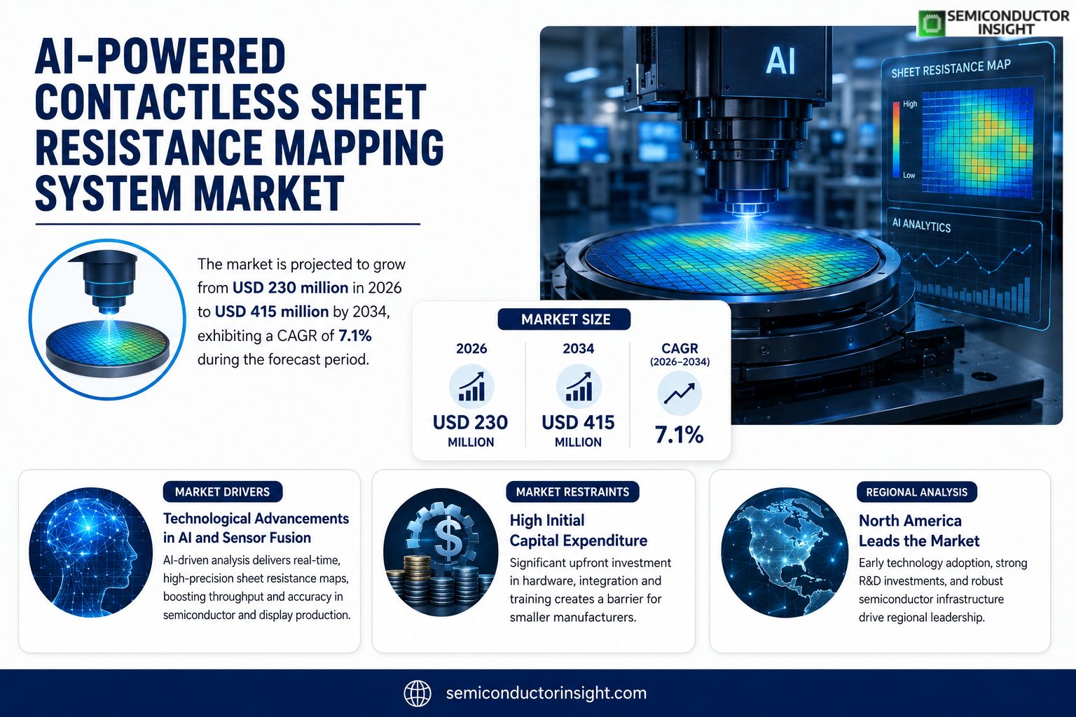
AI-Powered Contactless Sheet Resistance Mapping System market size was valued at USD 215 million in 2025. The market is projected to grow from USD 230 million in 2026 to USD 415 million by 2034, exhibiting a CAGR of 7.1% during the forecast period.
The AI‑Powered Contactless Sheet Resistance Mapping System is a non‑destructive metrology solution that employs laser‑based or optical scanning combined with advanced artificial‑intelligence algorithms to generate high‑resolution resistance maps of conductive films without physical probe contact. By interpreting reflected light patterns and thermal signatures, the system delivers rapid, repeatable measurements essential for thin‑film semiconductor and display manufacturing.The market is accelerating because semiconductor fabs are seeking higher throughput and lower defect rates, while emerging flexible electronics demand gentle inspection techniques. Furthermore, integration of machine‑learning analytics enables predictive process control, reducing waste and cycle time. Key players such as KLA Corporation, Applied Materials, Tokyo Electron Limited and NXP Semiconductors are expanding their portfolios through strategic R&D investments and partnerships with AI software firms.
MARKET DRIVERS
Technological Advancements in AI and Sensor Fusion
The rapid evolution of artificial‑intelligence algorithms enables real‑time analysis of sheet resistance without physical contact, dramatically improving measurement speed and precision. AI‑driven pattern recognition reduces operator error and supports high‑throughput production lines in semiconductor and display manufacturing.
Growing Demand for Non‑Destructive Testing
Manufacturers are increasingly prioritising non‑destructive evaluation to protect delicate substrates. The AI‑Powered Contactless Sheet Resistance Mapping System Market benefits from this shift, as contactless solutions avoid surface damage and enable continuous monitoring during process runs.
➤ “Adoption of contactless, AI‑based mapping tools is accelerating, with more than 60 % of leading fabs planning upgrades within the next two years.”
Regulatory trends emphasizing product reliability also drive investment. Compliance frameworks now require tighter control of electrical uniformity, prompting firms to install advanced mapping systems that generate traceable data for audits.
MARKET CHALLENGES
High Initial Capital Expenditure
Deploying AI‑Powered Contactless Sheet Resistance Mapping System Market solutions often involves significant upfront costs for hardware, integration, and staff training. Smaller manufacturers may struggle to justify the expense without clear short‑term ROI, slowing broader market penetration.
Other Challenges
Data Integration Complexity
Integrating the high‑volume data streams from contactless sensors into existing Manufacturing Execution Systems (MES) can be technically demanding, requiring customized middleware and robust cybersecurity measures.
MARKET RESTRAINTS
Limited Skilled Workforce
The sophisticated AI models underpinning the AI‑Powered Contactless Sheet Resistance Mapping System Market demand expertise in both data science and electrical metrology. A shortage of professionals who can operate, calibrate, and maintain these systems creates a bottleneck for rapid adoption.
MARKET OPPORTUNITIES
Expansion into Emerging Verticals
Beyond traditional semiconductor and display sectors, industries such as flexible wearable electronics, solar photovoltaics, and automotive lighting are beginning to recognize the value of contactless sheet‑resistance mapping. Targeted solutions tailored to these niches open new revenue streams for vendors.
AI Model Commercialization
Software‑as‑a‑service (SaaS) offerings that license AI analysis engines provide a lower‑cost entry point, allowing customers to upgrade capabilities without replacing hardware. This business model is expected to accelerate market growth while mitigating capital barriers.
AI-Powered Contactless Sheet Resistance Mapping System Market Trends
Rising Throughput Demands in Semiconductor Fab
The AI-Powered Contactless Sheet Resistance Mapping System is increasingly adopted in semiconductor fabrication lines where manufacturers strive for higher throughput while maintaining sub‑micron defect thresholds. By scanning conductive films with laser‑based or optical sensors and applying sophisticated AI algorithms, the solution delivers high‑resolution resistance maps within seconds, eliminating the time‑consuming probe‑touch methods traditionally used. The rapid, repeatable measurements support real‑time feedback loops, allowing process engineers to identify sheet resistance deviations before they propagate into yield loss. Because the technique is non‑destructive, it integrates seamlessly with existing in‑line inspection stations, preserving wafer integrity and reducing downtime. This combination of speed, accuracy, and safety underpins the market’s momentum across major semiconductor fabs.
Other Trends
Flexible Electronics Inspection
Flexible electronics represent a fast‑growing segment that imposes distinct inspection challenges. Thin, bendable conductive layers cannot tolerate the mechanical stress of conventional contact‑based metrology, making a contactless approach essential. The AI‑driven mapping system captures reflected light patterns and thermal signatures from these delicate films, producing detailed resistance distributions without physical interaction. Manufacturers of flexible displays, wearable sensors, and roll‑to‑roll printed circuits are leveraging this capability to verify material uniformity and to qualify new substrates. The non‑invasive nature also enables frequent sampling during production, which improves statistical confidence while maintaining product reliability. As the flexible market expands, demand for such gentle yet precise measurement tools is expected to rise steadily.
AI-Enhanced Predictive Process Control
Integration of machine‑learning analytics transforms raw resistance data into actionable process insights. Predictive process control algorithms analyze trends across successive scans, flagging potential drift and recommending corrective actions before equipment tuning is required. This proactive stance reduces scrap rates, shortens cycle time, and supports tighter control of thin‑film thickness and composition. Leading vendors—including KLA Corporation, Applied Materials, Tokyo Electron Limited and NXP Semiconductors—are investing in AI software partnerships and dedicated R&D programs to embed these capabilities directly into their metrology platforms. Their combined efforts accelerate adoption across both mature and emerging manufacturing lines, reinforcing the overall growth trajectory of the AI‑Powered Contactless Sheet Resistance Mapping System Market.
COMPETITIVE LANDSCAPE
Key Industry Players
AI‑Powered Contactless Sheet Resistance Mapping System Market Overview
The market is dominated by a handful of vertically integrated semiconductor equipment manufacturers that leverage deep photolithography and metrology expertise. KLA Corporation leads with a portfolio that couples high‑speed laser scanning and proprietary AI‑driven defect analytics, enabling wafer‑level resistance maps in sub‑minute cycles. Applied Materials follows closely, offering a modular system integrated with its broader process‑control suite, which accelerates adoption in fabs seeking end‑to‑end data pipelines. Tokyo Electron Limited and NXP Semiconductors complement the top tier by embedding AI‑enhanced optics into their thin‑film inspection lines, targeting high‑volume memory and display fabs. This concentration of capability creates an oligopolistic structure where the top four firms command the majority of revenue, while smaller innovators rely on niche differentiation and strategic collaborations with AI software specialists.Beyond the leading quartet, a diverse set of niche players enriches the ecosystem with specialized architectures and region‑focused offerings. ASML Holding supplies next‑generation extreme ultraviolet (EUV)‑compatible scanners that double as resistance mapping tools for advanced nodes. Nova Measuring Instruments and CSEM introduce compact, contactless solutions aimed at R&D labs and flexible‑electronics manufacturers, emphasizing low‑cost, high‑resolution mapping. Companies such as Lumerical (Ansys), Veeco Instruments, and Hitachi High‑Technologies provide optical‑profilometry hybrids that blend thermal signature analysis with AI, catering to emerging markets like wearable sensors and automotive displays. The presence of these agile firms sustains competitive pressure, fostering rapid innovation cycles and expanding the addressable market across both mature and leading‑edge semiconductor segments.
List of Key AI‑Powered Contactless Sheet Resistance Mapping System Companies Profiled
- KLA Corporation
- Applied Materials
- Tokyo Electron Limited
- NXP Semiconductors
- ASML Holding
- Nova Measuring Instruments
- CSEM
- Lumerical (Ansys)
- Veeco Instruments
- Hitachi High‑Technologies
- Advantest
- JSR Corporation
- Lam Research
- Teradyne
- imec
Segment Analysis:
| Segment Category | Sub-Segments | Key Insights |
| By Type |
|
Laser‑based optical scanning
|
| By Application |
|
Thin‑film semiconductor manufacturing
|
| By End User |
|
Semiconductor fabs
|
| By Technology |
|
AI‑enhanced image processing
|
| By Market Trend |
|
Shift toward contactless metrology
|
Regional Analysis: AI-Powered Contactless Sheet Resistance Mapping System Market
Early adoption of AI‑driven analytics and real‑time data processing distinguishes North American OEMs. Manufacturers integrate contactless sheet resistance mapping into inline metrology lines, enabling rapid defect identification and process optimization without compromising wafer integrity. This proactive approach accelerates cycle times and supports higher transistor densities in next‑generation chips.
Federal and state agencies provide clear guidelines for equipment safety and data security, fostering confidence among end‑users. Incentive programs for advanced manufacturing, such as the CHIPS Act, indirectly promote investment in contactless mapping technologies that align with national competitiveness objectives.
Leading firms, including KLA‑Tencor, Advantest, and Nova Measuring Instruments, leverage deep AI expertise to differentiate their offerings. Strategic partnerships with semiconductor fabs and academia accelerate product refinement, ensuring that solutions address real‑world production challenges.
Fab managers seek instruments that minimize physical contact while delivering sub‑micron resolution. The demand for scalable, software‑centric platforms that integrate seamlessly with existing manufacturing execution systems underscores the region’s preference for flexible, future‑proof solutions.
Europe
European semiconductor hubs, notably in Germany and the Netherlands, exhibit a measured yet progressive uptake of AI‑powered contactless sheet resistance mapping. Collaborative research programmes funded by the EU encourage cross‑border innovation, resulting in incremental improvements in data analytics and machine learning models. While adoption rates lag slightly behind North America, strict environmental regulations drive interest in non‑contact methods that reduce material waste and chemical usage. OEMs focus on integrating these systems within lean production lines to meet both quality and sustainability targets, aligning with the continent’s broader Industry 4.0 agenda.
Asia‑Pacific
The Asia‑Pacific region, anchored by manufacturing powerhouses in Taiwan, South Korea, and China, shows strong momentum due to high production volumes and cost‑sensitivity. Companies prioritize solutions that deliver rapid throughput and robust AI diagnostics to maintain competitiveness in the supply chain. Local vendors increasingly partner with Western technology leaders to incorporate advanced algorithms, while government initiatives such as China’s “Made in 2025” and South Korea’s “Smart Factory” programs provide financial support for adopting contactless metrology. The market dynamics reflect a balance between rapid scale‑up and the need for sophisticated defect detection capabilities.
South America
South American semiconductor activity remains nascent, yet emerging nano‑electronics research centers in Brazil and Chile are exploring AI‑enhanced sheet resistance mapping as part of broader efforts to attract high‑value manufacturing. The region’s emphasis on cost‑effective, scalable solutions drives interest in modular contactless systems that can be retrofitted to existing equipment. Government incentives aimed at technology transfer and skill development further encourage early‑stage pilots, positioning South America as a potential growth zone as supply chains diversify.
Middle East & Africa
In the Middle East and Africa, market activity is primarily driven by strategic investments in advanced manufacturing hubs, particularly in the United Arab Emirates and South Africa. Stakeholders view AI‑powered contactless mapping as a catalyst for establishing world‑class semiconductor fabs that meet stringent quality standards without extensive physical handling. Collaborative ventures with multinational equipment providers aim to build local expertise, while regional tech incubators focus on AI model development tailored to the unique process conditions of emerging fabs. Though still early in its adoption curve, the region’s commitment to innovation signals a steady upward trajectory.
Report Scope
This market research report provides a comprehensive analysis of the AI-Powered Contactless Sheet Resistance Mapping System Market , covering the forecast period 2026–2034. It offers detailed insights into market dynamics, technological advancements, competitive landscape, and key trends shaping the industry.
Key focus areas of the report include:
- Market Overview: The report begins with an overview outlining its current market scenario, key growth indicators, and industry transformation drivers. It discusses macroeconomic factors, demand–supply balance, regulatory landscape, and the strategic role of semiconductors in powering advancements across industries such as automotive, telecommunications, consumer electronics, and industrial automation.
- Market Size & Forecast: Historical data and future projections for revenue, unit shipments, and market value across major regions and segments.
- Segmentation Analysis: Detailed breakdown by product type, technology, application, and end-user industry to identify high-growth segments and investment opportunities.
- Regional Insights: Insights into market performance across North America, Europe, Asia-Pacific, Latin America, and the Middle East & Africa, including country-level analysis where relevant.
- Competitive Landscape: Profiles of leading market participants, including their product offerings, R&D focus, manufacturing capacity, pricing strategies, and recent developments such as mergers, acquisitions, and partnerships.
- Technology Trends & Innovation: Assessment of emerging technologies, integration of AI/IoT, semiconductor design trends, fabrication techniques, and evolving industry standards.
- Market Drivers & Restraints: Evaluation of factors driving market growth along with challenges, supply chain constraints, regulatory issues, and market-entry barriers.
- Stakeholder Insights: Insights for component suppliers, OEMs, system integrators, investors, and policymakers regarding the evolving ecosystem and strategic opportunities.
Primary and secondary research methods are employed, including interviews with industry experts, data from verified sources, and real-time market intelligence to ensure the accuracy and reliability of the insights presented.
FREQUENTLY ASKED QUESTIONS:
What is the current market size of AI-Powered Contactless Sheet Resistance Mapping System Market?
-> AI-Powered Contactless Sheet Resistance Mapping System Market was valued at USD 215 million in 2025 and is expected to reach USD 415 million by 2034.
Which key companies operate in AI-Powered Contactless Sheet Resistance Mapping System Market?
-> Key players include KLA Corporation, Applied Materials, Tokyo Electron Limited, and NXP Semiconductors, among others.
What are the key growth drivers?
-> Key growth drivers include semiconductor fabs seeking higher throughput and lower defect rates, emerging flexible electronics demanding gentle inspection, and integration of machine‑learning analytics for predictive process control.
Which region dominates the market?
-> Regional dominance information is not disclosed in the available source.
What are the emerging trends?
-> Emerging trends include AI‑driven predictive analytics, flexible electronics inspection, and advanced non‑destructive metrology techniques.
Get Sample Report PDF for Exclusive Insights
Report Sample Includes
- Table of Contents
- List of Tables & Figures
- Charts, Research Methodology, and more...
 Download Sample Report PDF




