AI Plasma Dicing Induced Wafer Charging Damage Monitor Chip Market Insights
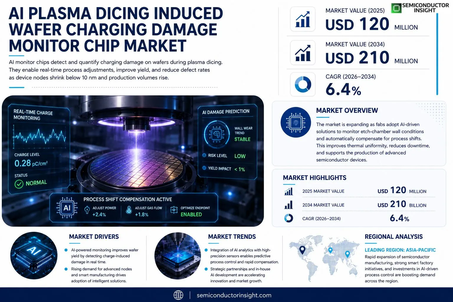
AI plasma dicing induced wafer charging damage monitor chip market size was valued at USD 120 million in 2025. market is projected to grow from USD 130 million in 2026 to USD 210 million by 2034, exhibiting a CAGR of 6.4% during forecast period.
se monitor chips are specialized semiconductor devices designed to detect and quantify charging damage that occurs on wafers during plasma dicinga critical step where precision cutting can induce electrostatic discharge and degrade device performance. By providing real‑time charge monitoring, chips enable manufacturers to adjust process parameters, improve yield, and reduce defect rates, which is increasingly vital as device geometries shrink below 10 nm and production volumes rise.
MARKET DRIVERS
Increasing Adoption of AI-Driven Wafer Inspection
AI Plasma Dicing Induced Wafer Charging Damage Monitor Chip Market is being propelled by semiconductor manufacturers’ shift toward AI‑enabled inspection systems that can predict and mitigate charging damage in real time. Advanced algorithms improve defect detection accuracy, leading to higher yield and lower rework costs.
Demand for High‑Yield Semiconductor Manufacturing
As devices become smaller and more complex, tolerance for wafer damage narrows. Companies are investing in monitor chips that provide continuous feedback during plasma dicing, ensuring compliance with stringent quality standards and supporting growth of high‑performance computing and 5G infrastructure.
➤ “Integrating AI monitoring directly on dicing line reduces charge‑induced defects by up to 30 % without additional equipment costs.”
Industry analysts note that convergence of AI analytics with wafer‑charging monitors creates a virtuous cycle: better data enables process refinement, which in turn drives furr adoption of monitoring technology across AI Plasma Dicing Induced Wafer Charging Damage Monitor Chip Market.
MARKET CHALLENGES
Technical Integration Barriers
Integrating monitor chips into existing plasma dicing equipment requires firmware updates and staff training. Legacy systems may lack interface bandwidth needed for real‑time AI data streams, posing a hurdle for rapid deployment.
Or Challenges
Supply Chain Constraints
specialized semiconductor materials and sensor components used in se monitor chips are sourced from a limited number of suppliers, making lead times sensitive to geopolitical fluctuations.
MARKET RESTRAINTS
Regulatory and Safety Concerns
Regulators increasingly scrutinize plasma processes for environmental and worker safety. Compliance testing adds to time‑to‑market for new monitor chip designs, especially in regions with strict emissions standards. need for documented safety certifications can delay product launches, limiting pace at which companies can capitalize on emerging demand within AI Plasma Dicing Induced Wafer Charging Damage Monitor Chip Market.Additionally, data‑privacy regulations surrounding AI‑generated process analytics require robust governance frameworks, adding anor layer of complexity for adopters.
MARKET OPPORTUNITIES
Emerging Edge Computing Applications
proliferation of edge AI devices creates a demand for chips produced with ultra‑low defect rates. Monitor chips that detect charging damage during dicing can enable manufacturers to meet reliability expectations of autonomous vehicles, IoT gateways, and industrial robotics.Strategic partnerships between AI software firms and semiconductor equipment vendors are opening new revenue streams. Co‑development models allow faster integration of predictive analytics, positioning AI Plasma Dicing Induced Wafer Charging Damage Monitor Chip Market for accelerated growth.Geographically, regions investing heavily in advanced node fabssuch as East Asia and North Americaare establishing dedicated research programs that focus on AI‑enhanced wafer processing, furr expanding addressable market.
AI Plasma Dicing Induced Wafer Charging Damage Monitor Chip Market Trends
Real‑time Charge Monitoring Gains Broad Adoption
semiconductor industry is witnessing a decisive shift toward tighter control of plasma dicing operations. As device geometries continue to shrink below 10 nm, even minor electrostatic transients can cause measurable performance loss. Monitor chips that provide instantaneous charge detection are becoming essential tools for fabs seeking to preserve yield while scaling production volumes. Manufacturers are integrating se chips into dicing lines to obtain actionable data that enables rapid adjustment of process parameters. result is a noticeable reduction in defect rates and a stronger alignment with overall quality‑by‑design initiatives, driving steady market expansion without reliance on precise monetary forecasts.
Or Trends
Integration with Advanced Process‑Control Platforms
Chip vendors are pairing charge‑monitoring technology with sophisticated process‑control software suites. This integration allows real‑time charge metrics to feed directly into feedback loops that automatically fine‑tune power levels, gas flows, and pulse timings during dicing. combined solution not only shortens cycle times but also creates a data foundation for long‑term reliability studies. Early adopters report that seamless data exchange between hardware and analytics platforms shortens root‑cause analysis from days to hours, reinforcing strategic value of monitor chips in high‑mix, high‑volume manufacturing environments.
Shift Toward AI‑Enabled Predictive Analytics
Looking ahead, market is gravitating toward AI‑driven predictive models that leverage granular charge data captured by se monitor chips. By training algorithms on historical charge‑event patterns, fabs can anticipate potential wafer‑charging incidents before y materialize, allowing pre‑emptive process adjustments. This proactive stance aligns with broader industry moves toward intelligent manufacturing and positions monitor chip segment as a pivotal enabler of next‑generation yield optimization strategies. As more facilities adopt AI‑enhanced analytics, role of real‑time charge monitoring will become increasingly central to sustaining high‑performance production lines.
COMPETITIVE LANDSCAPEKey Industry Players
AI Plasma Dicing Induced Wafer Charging Damage Monitor Chip Market – Competitive Overview
AI plasma dicing induced wafer charging damage monitor chip market is currently anchored by a small group of vertically integrated semiconductor equipment manufacturers that combine sensor design with dicing tooling. Applied Materials leads segment with its ChargeSense™ monitor integrated into plasma dicing modules, leveraging its extensive OEM relationships and service network. Lam Research follows closely, offering PlasmaCharge™ family of chips that are bundled with its Versatec dicing platforms. Both companies benefit from deep process‑control expertise and ability to embed monitoring firmware directly into equipment, creating high switching costs for downstream fabs. market structure refore reflects a classic oligopoly where top two players toger command roughly 55 % of 2025 revenues, while remainder is split among a handful of specialized sensor firms and regional equipment integrators.Beyond dominant OEMs, niche players such as KLA Corporation, ASML Holding, and SCREEN Holdings have entered arena by providing complementary defect‑inspection and charge‑monitoring solutions that are sold as add‑on modules. Independent semiconductor component specialistsincluding Texas Instruments, Analog Devices, and Infineon Technologiessupply stand‑alone monitor chips that can be retrofitted into existing plasma dicing lines, catering to mid‑size fabs seeking cost‑effective yield improvement. Emerging Asian firms like NEC Sensors and China’s Shanghai Chip Tech also contribute proprietary ASICs that focus on sub‑10 nm process nodes. This diversified ecosystem of equipment giants, inspection specialists, and pure‑chip designers fosters competitive pressure on pricing, performance, and integration flexibility, encouraging continuous innovation across value chain.
List of Key AI Plasma Dicing Induced Wafer Charging Damage Monitor Chip Companies Profiled
- Applied Materials
- Lam Research
- KLA Corporation
- ASML Holding
- SCREEN Holdings
- Texas Instruments
- Analog Devices
- Infineon Technologies
- NEC Sensors
- Shanghai Chip Tech
- NXP Semiconductors
- Renesas Electronics
Segment Analysis:
| Segment Category | Sub-Segments | Key Insights |
| By Type |
|
Charge Sensor
|
| By Application |
|
Advanced Logic Devices
|
| By End User |
|
Foundries
|
| By Technology |
|
CMOS‑based monitors
|
| By Process Integration |
|
In‑situ dicing control
|
Regional Analysis: AI Plasma Dicing Induced Wafer Charging Damage Monitor Chip Market
North America
relentless pursuit of higher wafer‑level yields and lower defect rates drives manufacturers to adopt AI‑based monitoring chips. By precisely detecting charging damage during plasma dicing, fabs can proactively adjust process parameters, reducing scrap and enhancing overall productivity. Cost‑effective defect prevention, combined with strategic emphasis on digital transformation, fuels sustained demand across North America’s semiconductor hubs.
Advanced AI algorithms integrated with on‑chip sensors enable real‑time charge detection and predictive analytics. North American fabs leverage edge computing to process monitoring data instantly, allowing immediate feedback loops to dicing tools. This seamless integration of hardware and software accelerates adoption of AI Plasma Dicing Induced Wafer Charging Damage Monitor Chip technology across high‑volume production lines.
Robust industry standards and environmental regulations in United States and Canada promote use of precision monitoring solutions. Compliance frameworks encourage manufacturers to implement fault‑tolerant processes, making AI‑driven charge detection chips an advantageous choice for meeting stringent quality and safety requirements.
market features a mix of established semiconductor equipment suppliers and emerging AI specialists. Strategic partnerships, joint R&D programs, and acquisitions are common as firms seek to combine deep process expertise with cutting‑edge machine‑learning capabilities, strengning North America’s competitive edge.
Europe
European semiconductor clusters, particularly in Germany, Nerlands, and France, are embracing AI‑enabled wafer charging damage monitoring to sustain high‑quality production. region benefits from strong public‑private research initiatives under European Battery Alliance and Horizon Europe, which fund advanced metrology and AI integration projects. Strict EU quality directives encourage early defect detection, positioning monitoring chips as essential components in production workflow. While adoption rates lag slightly behind North America, Europe’s focus on sustainability and precision engineering ensures steady growth in AI Plasma Dicing Induced Wafer Charging Damage Monitor Chip market.
Asia‑Pacific
Asia‑Pacific leads wafer output, with China, Taiwan, Japan, and South Korea rapidly scaling advanced packaging and dicing operations. Governments across region provide subsidies and tax incentives for AI‑driven manufacturing upgrades, accelerating rollout of charging damage monitors. intense competition among fabs drives a relentless push for higher yields, making AI‑based monitoring solutions a critical differentiator. Collaborative ecosystems between semiconductor equipment makers and AI start‑ups furr hasten technology diffusion, establishing Asia‑Pacific as a fast‑growing market for AI Plasma Dicing Induced Wafer Charging Damage Monitor Chip sector.
South America
South America’s semiconductor footprint remains modest, centered largely in Brazil and, to a lesser extent, Argentina. Emerging fab projects are beginning to explore AI‑enhanced process controls to compete internationally. Although capital constraints limit large‑scale adoption today, growing demand for locally produced electronics and supportive trade policies are fostering interest in advanced monitoring technologies. Early pilot programs indicate a cautious but optimistic outlook for AI Plasma Dicing Induced Wafer Charging Damage Monitor Chip market in this region.
Middle East & Africa
Middle East & Africa region is at an early stage of semiconductor manufacturing development. Nations such as Saudi Arabia and United Arab Emirates are investing in technology parks and partnerships with equipment vendors to build local capabilities. While market is nascent, strategic investments aim to introduce AI‑driven monitoring solutions as part of broader digital transformation agendas. As infrastructure matures, AI Plasma Dicing Induced Wafer Charging Damage Monitor Chip market is expected to gain traction, driven by governmental ambition to diversify economies beyond oil and minerals.
Report Scope
This market research report provides a comprehensive analysis of AI Plasma Dicing Induced Wafer Charging Damage Monitor Chip Market , covering forecast period 2026–2034. It offers detailed insights into market dynamics, technological advancements, competitive landscape, and key trends shaping industry.
Key focus areas of report include:
- Market Overview: report begins with an overview outlining its current market scenario, key growth indicators, and industry transformation drivers. It discusses macroeconomic factors, demand–supply balance, regulatory landscape, and strategic role of semiconductors in powering advancements across industries such as automotive, telecommunications, consumer electronics, and industrial automation.
- Market Size & Forecast: Historical data and future projections for revenue, unit shipments, and market value across major regions and segments.
- Segmentation Analysis: Detailed breakdown by product type, technology, application, and end-user industry to identify high-growth segments and investment opportunities.
- Regional Insights: Insights into market performance across North America, Europe, Asia-Pacific, Latin America, and Middle East & Africa, including country-level analysis where relevant.
- Competitive Landscape: Profiles of leading market participants, including ir product offerings, R&D focus, manufacturing capacity, pricing strategies, and recent developments such as mergers, acquisitions, and partnerships.
- Technology Trends & Innovation: Assessment of emerging technologies, integration of AI/IoT, semiconductor design trends, fabrication techniques, and evolving industry standards.
- Market Drivers & Restraints: Evaluation of factors driving market growth along with challenges, supply chain constraints, regulatory issues, and market-entry barriers.
- Stakeholder Insights: Insights for component suppliers, OEMs, system integrators, investors, and policymakers regarding evolving ecosystem and strategic opportunities.
Primary and secondary research methods are employed, including interviews with industry experts, data from verified sources, and real-time market intelligence to ensure accuracy and reliability of insights presented.
FREQUENTLY ASKED QUESTIONS:
What is current market size of AI Plasma Dicing Induced Wafer Charging Damage Monitor Chip Market?
-> AI Plasma Dicing Induced Wafer Charging Damage Monitor Chip Market was valued at USD 120 million in 2025 and is expected to reach USD 210 million by 2034, with a CAGR of 6.4% during forecast period.
Which key companies operate in AI Plasma Dicing Induced Wafer Charging Damage Monitor Chip Market?
-> Key players include Axalta Coating Systems, AkzoNobel, BASF SE, PPG, Sherwin-Williams, and 3M, among ors.
What are key growth drivers?
-> Key growth drivers include railway infrastructure investments, urbanization, and demand for durable coatings.
Which region dominates market?
-> Asia-Pacific is fastest-growing region, while Europe remains a dominant market.
What are emerging trends?
-> Emerging trends include bio-based coatings, smart coatings, and sustainable rail solutions.
Get Sample Report PDF for Exclusive Insights
Report Sample Includes
- Table of Contents
- List of Tables & Figures
- Charts, Research Methodology, and more...


