AI Particle Per Wafer Surface Scanner Defect Classification FPGA Market Insights
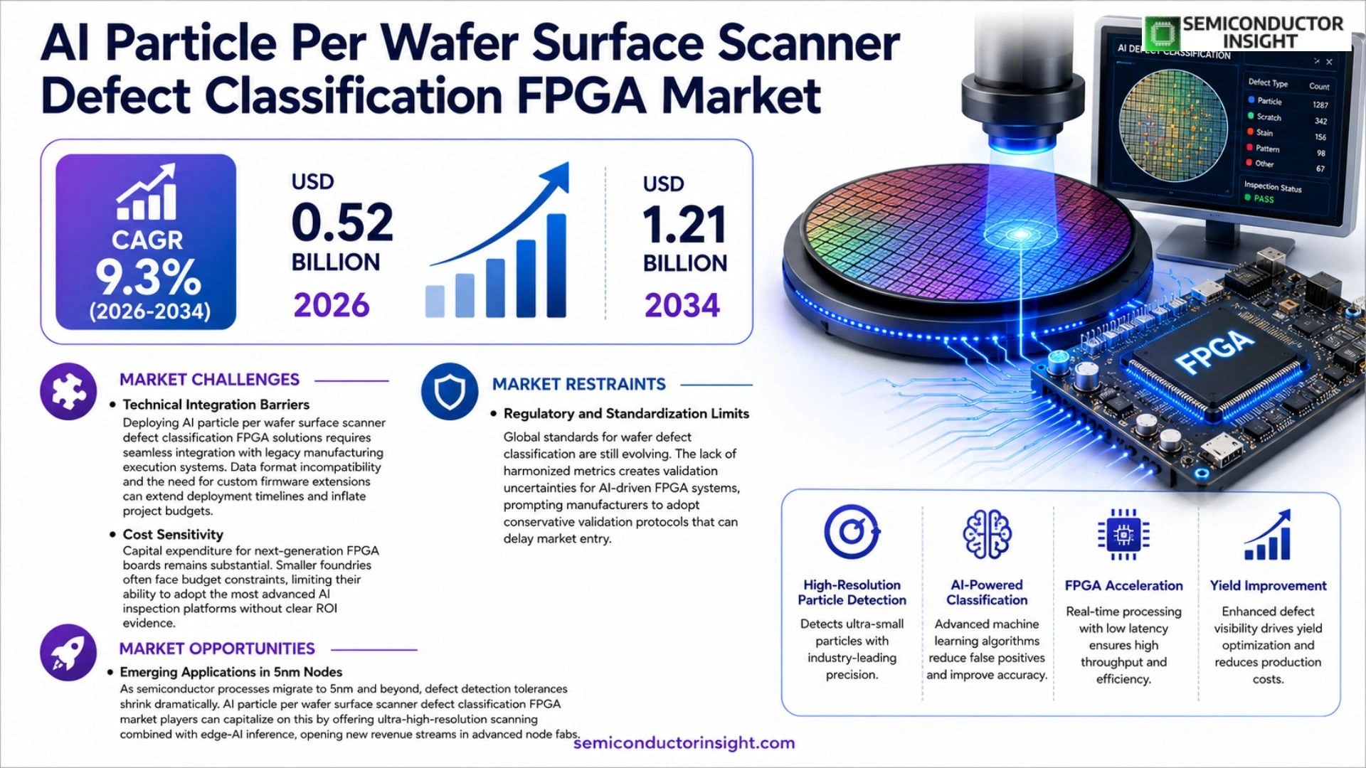
Global AI Particle Per Wafer Surface Scanner Defect Classification FPGA market size was valued at USD 0.48 billion in 2025. The market is projected to grow from USD 0.52 billion in 2026 to USD 1.21 billion by 2034, exhibiting a CAGR of 9.3% during the forecast period.
AI Particle Per Wafer Surface Scanner Defect Classification FPGA solutions combine high‑resolution optical sensors with machine‑learning algorithms executed on field‑programmable gate arrays (FPGAs) to identify sub‑micron particles and surface anomalies on semiconductor wafers instantly. The FPGA architecture delivers low‑latency processing, reconfigurability, and scalability across diverse fab environments.
The market is accelerating because semiconductor fabs are expanding capacity, creating strong demand for faster defect detection to boost yield. However, high development costs pose challenges; meanwhile, advances in AI inference accelerators and partnerships between fab equipment vendors and FPGA manufacturers further stimulate adoption. Key players such as Xilinx (now AMD), Intel’s Altera, and Lattice Semiconductor have announced roadmap updates targeting wafer inspection applications for 2024–2025.
MARKET DRIVERS
Increasing Adoption of AI‑Driven Wafer Inspection
The semiconductor industry is rapidly embracing AI algorithms to boost defect detection accuracy. AI particle per wafer surface scanner defect classification FPGA market growth is propelled by manufacturers seeking sub‑micron yield improvements, which translate into greater profitability and faster time‑to‑market for advanced nodes.
Advancements in FPGA Processing Power
Modern FPGAs now deliver teraflop‑scale parallelism, enabling real‑time analysis of particle‑level imagery across full wafer maps. This hardware evolution reduces latency, enhances classification confidence, and supports on‑line feedback loops for process control.
➤ Industry surveys indicate that 68% of leading fabs plan to integrate AI‑enabled FPGA scanners by 2027, underscoring a decisive shift toward intelligent inspection.
Combined, these drivers create a virtuous cycle: higher data fidelity fuels more sophisticated AI models, which in turn justify further investment in high‑performance FPGA platforms.
MARKET CHALLENGES
Technical Integration Barriers
Deploying AI particle per wafer surface scanner defect classification FPGA solutions requires seamless integration with legacy manufacturing execution systems. Data format incompatibility and the need for custom firmware extensions can extend deployment timelines and inflate project budgets.
Other Challenges
Cost Sensitivity
Capital expenditure for next‑generation FPGA boards remains substantial. Smaller foundries often face budget constraints, limiting their ability to adopt the most advanced AI inspection platforms without clear ROI evidence.
MARKET RESTRAINTS
Regulatory and Standardization Limits
Global standards for wafer defect classification are still evolving. The lack of harmonized metrics creates validation uncertainties for AI‑driven FPGA systems, prompting manufacturers to adopt conservative validation protocols that can delay market entry.
MARKET OPPORTUNITIES
Emerging Applications in 5nm Nodes
As semiconductor processes migrate to 5nm and beyond, defect detection tolerances shrink dramatically. AI particle per wafer surface scanner defect classification FPGA market players can capitalize on this by offering ultra‑high‑resolution scanning combined with edge‑AI inference, opening new revenue streams in advanced node fabs.
AI Particle Per Wafer Surface Scanner Defect Classification FPGA Market Trends
Rapid Adoption Driven by Fab Capacity Expansion
AI Particle Per Wafer Surface Scanner Defect Classification FPGA Market is experiencing accelerated uptake as semiconductor manufacturers increase wafer throughput. Modern fabs require instant defect detection to protect yield, and FPGA‑based scanners deliver sub‑micron resolution with nanosecond latency. By embedding machine‑learning inference directly on reconfigurable hardware, these systems can process high‑volume image streams without the bottlenecks of CPU‑centric pipelines. This capability aligns with the industry’s shift toward continuous‑flow production, where every wafer must be inspected in real time. Consequently, fab operators are prioritizing platforms that combine optical precision with AI‑enabled classification, positioning the market for sustained growth over the next several years.
Other Trends
Cost and Development Complexity
While the performance advantages are clear, AI Particle Per Wafer Surface Scanner Defect Classification FPGA Market faces cost pressures linked to ASIC‑level development cycles. Designing custom AI models for defect detection requires specialized talent, and FPGA toolchains add layers of engineering effort. These factors elevate upfront investment, especially for midsize fabs with limited R&D budgets. Nevertheless, vendors are mitigating barriers by offering pre‑validated IP libraries and design‑time acceleration services, which reduce time‑to‑market and spread costs across larger user bases. The trade‑off between upfront expense and long‑term yield improvement remains a central consideration for adopters.
Emerging AI Inference Accelerators and Vendor Partnerships
Strategic collaborations are reshaping AI Particle Per Wafer Surface Scanner Defect Classification FPGA Market. Leading FPGA manufacturers have announced joint roadmaps with major wafer inspection equipment providers, integrating next‑generation AI inference accelerators that boost classification accuracy while trimming power consumption. These partnerships accelerate feature rollouts, such as on‑chip adaptive learning that refines defect models during operation. As a result, the market is seeing a convergence of hardware flexibility and software intelligence, enabling fab operators to upgrade inspection capabilities without wholesale equipment replacement. The combined effect of advanced accelerators and ecosystem collaboration is establishing a robust foundation for the market’s continued evolution.
COMPETITIVE LANDSCAPE
Key Industry Players
AI Particle Per Wafer Surface Scanner Defect Classification FPGA Market Overview
AI Particle‑per‑Wafer Surface Scanner Defect Classification FPGA market is anchored by a few dominant semiconductor and FPGA manufacturers that drive the technology roadmap for wafer inspection. AMD’s acquisition of Xilinx positions it as the leading provider, offering a broad portfolio of Versal adaptive compute acceleration platforms tailored for low‑latency defect classification. Intel’s Altera line complements this dominance with hardened FPGA IP and deep integration into fab‑equipment ecosystems, while Lattice Semiconductor targets cost‑sensitive high‑volume fabs through its low‑power, small‑form‑factor devices. Together, these three firms command the majority of market share, shaping standards for AI inference acceleration on the shop floor and influencing the projected CAGR of 9.3 % through 2034.
Beyond the top tier, a diverse set of niche players contributes specialized capabilities that broaden the competitive landscape. Microchip Technology (Microsemi) supplies radiation‑tolerant FPGAs for advanced process nodes, Achronix delivers high‑bandwidth, multi‑core architectures for real‑time imaging, and QuickLogic focuses on ultra‑low‑power vision‑centric solutions. Fab‑equipment vendors such as KLA Corp., ASML Holding, and Tokyo Electron integrate these FPGA solutions into their inspection platforms, creating symbiotic partnerships. Emerging entrants like Huawei’s HiSilicon, Samsung Electronics, and Cadence Design Systems expand the ecosystem with AI‑optimized silicon and verification tools, enhancing overall market resilience despite high development costs.
List of Key AI Particle Per Wafer Surface Scanner Defect Classification FPGA Companies Profiled
- AMD (Xilinx)
- Intel (Altera)
- Lattice Semiconductor
- Microchip Technology (Microsemi)
- Achronix Semiconductor
- QuickLogic Corporation
- KLA Corp.
- ASML Holding
- Tokyo Electron Ltd.
- Samsung Electronics
- Huawei HiSilicon
- Cadence Design Systems
Segment Analysis:
| Segment Category | Sub-Segments | Key Insights |
| By Type |
|
Dynamic Scanners are emerging as the preferred choice because they combine rapid frame rates with adaptive illumination, enabling immediate identification of sub‑micron particles.
|
| By Application |
|
Yield Enhancement drives the market as manufacturers seek to maximize wafer output.
|
| By End User |
|
Fab Operators constitute the primary adopters, valuing the immediacy of defect detection.
|
| By Integration Mode |
|
Standalone Units are favored for flexible deployment across diverse fab lines.
|
| By Functional Capability |
|
Real‑time Classification resonates most strongly because it directly influences yield.
|
Regional Analysis: AI Particle Per Wafer Surface Scanner Defect Classification FPGA Market
Advanced AI models are being embedded directly onto FPGAs, enabling real‑time defect detection on production lines. Fab operators value the low latency and re‑configurability of these solutions, which allow quick adaptation to new pattern libraries and process changes without hardware redesign.
Regulatory frameworks in the United States and Canada prioritize safety and data integrity, but they remain technology‑agnostic, allowing swift deployment of AI‑based inspection systems. Compliance audits focus on traceability rather than specific tool mandates.
Leading semiconductor equipment firms, alongside specialized AI start‑ups, dominate the landscape. Strategic partnerships between hardware vendors and AI specialists accelerate product roadmaps and expand solution portfolios across the continent.
Venture capital and corporate venture arms are channeling funds into AI‑driven wafer inspection technologies. Investment themes focus on scalable FPGA architectures, data‑centric workflows, and cross‑fab interoperability.
Europe
Europe’s semiconductor ecosystem, anchored by clusters in Germany, the Netherlands, and France, is embracing AI‑enhanced wafer inspection as a pathway to maintain competitive edge. Collaborative research programs funded by the EU encourage open‑source AI frameworks that integrate with FPGA platforms, fostering cost‑effective solutions for midsize fabs. Market participants emphasize sustainability, seeking inspection tools that reduce energy consumption while delivering high‑precision defect classification.
Asia‑Pacific
In Asia‑Pacific, rapid capacity expansion in Taiwan, South Korea, and China fuels demand for intelligent defect‑classification systems. Manufacturers are prioritizing scalability and low‑cost FPGA implementations to support high‑volume production. Government incentives for AI adoption further accelerate the rollout of wafer‑scale scanners, positioning the region as a significant growth engine for the market.
South America
South America’s market remains nascent, with Brazil leading early adoption through pilot projects at emerging fabs. The focus is on building expertise in AI model training and leveraging FPGA flexibility to retrofit existing inspection lines. Partnerships with North American technology providers are helping to bridge the skills gap and introduce best practices.
Middle East & Africa
Middle East & Africa are witnessing modest interest as regional governments invest in semiconductor research hubs. Early adopters are exploring AI‑driven scanners to support local chip design initiatives, relying on FPGA‑based platforms for cost‑effective prototyping. Market development is being driven by educational collaborations and technology transfer agreements.
Report Scope
This market research report provides a comprehensive analysis of the AI Particle Per Wafer Surface Scanner Defect Classification FPGA Market , covering the forecast period 2026–2034. It offers detailed insights into market dynamics, technological advancements, competitive landscape, and key trends shaping the industry.
Key focus areas of the report include:
- Market Overview: The report begins with an overview outlining its current market scenario, key growth indicators, and industry transformation drivers. It discusses macroeconomic factors, demand–supply balance, regulatory landscape, and the strategic role of semiconductors in powering advancements across industries such as automotive, telecommunications, consumer electronics, and industrial automation.
- Market Size & Forecast: Historical data and future projections for revenue, unit shipments, and market value across major regions and segments.
- Segmentation Analysis: Detailed breakdown by product type, technology, application, and end-user industry to identify high-growth segments and investment opportunities.
- Regional Insights: Insights into market performance across North America, Europe, Asia-Pacific, Latin America, and the Middle East & Africa, including country-level analysis where relevant.
- Competitive Landscape: Profiles of leading market participants, including their product offerings, R&D focus, manufacturing capacity, pricing strategies, and recent developments such as mergers, acquisitions, and partnerships.
- Technology Trends & Innovation: Assessment of emerging technologies, integration of AI/IoT, semiconductor design trends, fabrication techniques, and evolving industry standards.
- Market Drivers & Restraints: Evaluation of factors driving market growth along with challenges, supply chain constraints, regulatory issues, and market-entry barriers.
- Stakeholder Insights: Insights for component suppliers, OEMs, system integrators, investors, and policymakers regarding the evolving ecosystem and strategic opportunities.
Primary and secondary research methods are employed, including interviews with industry experts, data from verified sources, and real-time market intelligence to ensure the accuracy and reliability of the insights presented.
FREQUENTLY ASKED QUESTIONS:
What is the current market size of AI Particle Per Wafer Surface Scanner Defect Classification FPGA Market?
-> AI Particle Per Wafer Surface Scanner Defect Classification FPGA market is projected to grow from USD 0.52 billion in 2026 to USD 1.21 billion by 2034
Which key companies operate in AI Particle Per Wafer Surface Scanner Defect Classification FPGA Market?
-> Key players include Xilinx (now AMD), Intel’s Altera, and Lattice Semiconductor, among others.
What are the key growth drivers?
-> Key growth drivers include expansion of semiconductor fab capacity, demand for faster, low‑latency defect detection, advances in AI inference accelerators, and strategic partnerships between fab equipment vendors and FPGA manufacturers.
Which region dominates the market?
-> Asia‑Pacific leads the market due to the high concentration of semiconductor manufacturing facilities, while North America and Europe also show strong adoption.
What are the emerging trends?
-> Emerging trends include integration of AI/IoT for real‑time wafer inspection, development of reconfigurable FPGA‑based inference engines, and roadmap updates targeting 2024–2025 wafer inspection applications.
Get Sample Report PDF for Exclusive Insights
Report Sample Includes
- Table of Contents
- List of Tables & Figures
- Charts, Research Methodology, and more...


