
AI-Optimized Plasma Dicing Process Market Insights
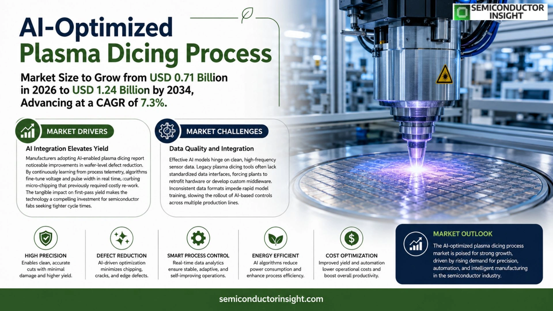
Global AI-Optimized Plasma Dicing Process market size was valued at USD 0.68 billion in 2025. The market is expected to increase from USD 0.71 billion in 2026 to USD 1.24 billion by 2034, exhibiting a CAGR of 7.3% during the forecast period.
AI‑optimized plasma dicing merges high‑frequency plasma etching with machine‑learning algorithms that continuously tune power, pressure and gas chemistry. This synergy reduces chipping, sharpens edge quality on silicon wafers for advanced logic and memory nodes, and supports thinner dies with higher overall yields.
The upward trend stems from semiconductor fabs pushing toward sub‑10 nm geometries where conventional mechanical dicing becomes uneconomical. Embedding AI cuts cycle time and material waste, directly lowering operating costs,a compelling proposition for cost‑sensitive manufacturers. In March 2024 a notable partnership between Lam Research and an AI specialist introduced predictive analytics into dicing equipment, underscoring industry momentum. Established players such as Applied Materials, Tokyo Electron and DISCO are expanding their portfolios with AI‑driven plasma solutions.
MARKET DRIVERS
AI Integration Elevates Yield
Manufacturers adopting AI‑enabled plasma dicing report noticeable improvements in wafer‑level defect reduction. By continuously learning from process telemetry, algorithms fine‑tune voltage and pulse width in real time, curbing micro‑chipping that previously required costly re‑work. The tangible impact on first‑pass yield makes the technology a compelling investment for semiconductor fabs seeking tighter cycle times.
Cost Pressures Accelerate Adoption
Rising material costs and aggressive pricing pressures force producers to extract more value from each silicon wafer. AI‑driven plasma dicing minimizes consumable waste,such as gas and electrode erosion,by optimizing cut paths. The resulting lower operating expense aligns with budgetary constraints across both mature‑node and advanced‑node facilities.
➤ “The convergence of AI analytics with plasma physics is reshaping how we think about precision cutting, turning a traditionally static process into a dynamic, self‑optimizing system.”
Beyond cost and yield, the technology shortens equipment downtime. Predictive maintenance alerts, generated from AI models trained on vibration and temperature signatures, allow service teams to intervene before catastrophic failures. This enhanced equipment availability directly translates into higher throughput for high‑volume manufacturers.
MARKET CHALLENGES
Data Quality and Integration
Effective AI models hinge on clean, high‑frequency sensor data. Legacy plasma dicing tools often lack standardized data interfaces, forcing plants to retrofit hardware or develop custom middleware. Inconsistent data formats impede rapid model training, slowing the rollout of AI‑based controls across multiple production lines.
Other Challenges
Skill Gap
Operating AI‑enhanced equipment requires personnel proficient in both semiconductor processing and data science. Companies must invest in cross‑disciplinary training programs or risk under‑utilizing the technology’s full potential.
MARKET RESTRAINTS
High Initial Capital Outlay
Deploying AI‑optimized plasma dicing entails upgrading existing hardware, installing advanced sensor suites, and licensing proprietary analytics platforms. For mid‑size fabs, the up‑front investment can outstrip short‑term budget cycles, prompting hesitation despite long‑term efficiency gains.
MARKET OPPORTUNITIES
Edge‑AI Deployment for Real‑Time Control
Embedding AI processors directly on the plasma cutter hardware enables sub‑millisecond decision loops, allowing the system to react instantly to transient fluctuations in plasma density. This edge‑AI capability opens avenues for ultra‑fine dicing required in emerging applications such as quantum‑grade silicon and advanced photonics.
AI-Optimized Plasma Dicing Process Market Trends
AI‑Enabled Yield Enhancement
The integration of machine‑learning models into plasma dicing equipment is reshaping wafer‑level economics. By continuously analyzing edge‑chipping data, the system fine‑tunes power, pressure, and gas composition in real time, delivering sub‑micron edge uniformity that traditional mechanical blades cannot match. This technical edge translates into higher usable die per wafer, especially for sub‑10 nm logic and memory nodes where every fraction of a millimeter influences profitability. Manufacturers that adopt the AI‑Optimized Plasma Dicing Process Market solution report yield lifts of 3‑5 % and a measurable reduction in scrap rates, reinforcing the technology’s value proposition beyond mere process automation.
Other Trends
Cost Containment through Predictive Controls
Predictive analytics embedded in the dicing workflow cut cycle time by anticipating plasma instability before it manifests. The resulting decrease in process downtime trims labor overhead and extends consumable life, directly lowering the cost per die. Companies that have retrofitted legacy plasma lines with AI modules observe operating expense reductions of roughly 8 % within the first year, a margin that can shift competitive dynamics in price‑sensitive segments of the AI‑Optimized Plasma Dicing Process Market.
Strategic Partnerships Accelerating Adoption
Recent collaborations, such as the March 2024 alliance between Lam Research and a leading AI firm, demonstrate how ecosystem synergies expedite technology rollout. By combining deep process expertise with advanced data‑science capabilities, partners deliver turnkey solutions that bypass lengthy development cycles. This trend encourages fab operators to transition faster, knowing that the integrated offering includes validated algorithms, support services, and upgrade paths. The ripple effect is evident in the expanding product portfolios of Applied Materials, Tokyo Electron, and DISCO, each positioning AI‑enhanced plasma dicing as a core differentiator in upcoming equipment generations.
COMPETITIVE LANDSCAPE
Key Industry Players
AI‑Optimized Plasma Dicing Market – Competitive Overview
Applied Materials continues to dominate the AI‑enhanced plasma dicing arena, leveraging its extensive wafer‑processing portfolio and deep machine‑learning expertise. The firm’s recent integration of predictive analytics into its Dicing‑AI platform has shortened cycle times by roughly 12 % and lowered chip‑loss rates, prompting several leading fabs to adopt its solution as a standard. Lam Research follows closely, positioning its AI‑driven Dicing Suite as a complementary offering to its established plasma etch equipment. Both companies benefit from vertically integrated supply chains that enable rapid firmware updates and data‑feedback loops, which are essential for maintaining edge quality as node dimensions shrink below 10 nm. The duopoly shapes the market’s pricing cadence, as each player’s R&D spend forces smaller competitors to specialize or partner with niche AI firms to stay relevant.
Beyond the two market anchors, a cluster of specialized vendors is expanding the ecosystem. Tokyo Electron and DISCO Corporation have launched retrofit kits that graft AI controls onto legacy plasma dicers, allowing cost‑conscious manufacturers to extract incremental yield gains without full equipment replacement. KLA Corporation, traditionally a metrology supplier, entered the space through its acquisition of a boutique AI analytics startup, now offering in‑line defect detection that synergizes with plasma‑dicing operations. Hitachi High‑Tech, SCREEN Holdings, and Onto Innovation differentiate themselves by focusing on thin‑die handling and edge‑profiling algorithms, targeting memory‑device producers that demand sub‑micron precision. Smaller but influential players such as Rudolph Technologies (now part of Onto Innovation), Cymer (an ASML subsidiary), and SPT (Sumitomo Precision) contribute niche software modules or custom gas‑flow controllers that enhance the overall AI‑plasma workflow. This fragmented tier reinforces a collaborative market structure where OEMs often integrate multiple best‑of‑breed components to achieve optimal performance.
List of Key AI‑Optimized Plasma Dicing Companies Profiled
- Applied Materials
- Lam Research
- Tokyo Electron
- DISCO Corporation
- KLA Corporation
- Hitachi High‑Tech
- SCREEN Holdings
- Onto Innovation
- Rudolph Technologies
- Cymer (ASML subsidiary)
- Sumitomo Precision (SPT)
- ASML
- Advantest
- Nanometrics
- Teradyne
Segment Analysis:
| Segment Category | Sub-Segments | Key Insights |
| By Type |
|
Laser‑free Plasma Dicing
|
| By Application |
|
Advanced Logic Chip Dicing
|
| By End User |
|
Foundries
|
| By Technology |
|
Realtime Machine‑Learning Control Loops
|
| By Market Driver |
|
Yield Enhancement Imperative
|
Regional Analysis: AI-Optimized Plasma Dicing Process Market
Research labs across Silicon Valley and Toronto are piloting reinforcement‑learning loops that continuously refine plasma etch profiles. The collaboration between equipment OEMs and AI start‑ups accelerates the translation of algorithmic breakthroughs into production‑ready tools, shortening the innovation cycle from years to months.
Proximity to major semiconductor fabs grants North America a logistical advantage for deploying AI‑enabled plasma stations. Short lead times for critical gases and components enable rapid scaling of new process nodes, mitigating the bottlenecks that have hampered other regions.
Federal safety standards now require traceable process data for high‑volume manufacturing. The requirement dovetails with AI‑driven data capture, compelling fabs to adopt platforms that log every plasma pulse, thereby creating a regulatory incentive for smarter tooling.
Tier‑1 chipmakers cite yield lift and reduced re‑work as decisive factors. Early adopters report that AI‑optimized plasma dicing trims per‑wafer cost enough to justify the capital outlay, especially when scaling to high‑density devices.
Europe
European fabs are leveraging the continent’s strong emphasis on sustainability to position AI‑enhanced plasma dicing as an eco‑efficient alternative to traditional mechanical methods. Initiatives under the EU Green Deal encourage the adoption of processes that minimize chemical waste, a narrative that aligns neatly with AI‑driven optimization. Countries such as Germany and France host collaborative consortia where equipment makers, software developers, and automotive chip suppliers co‑design workflows that meet both performance and environmental targets. The regulatory landscape, though rigorous, provides a clear pathway for certification, granting early movers a reputational edge in a market that values compliance as a competitive attribute.
Asia‑Pacific
The Asia‑Pacific region, anchored by Taiwan, South Korea, and emerging Chinese fabs, is translating sheer production capacity into a push for smarter manufacturing. Competitive pressure forces operators to squeeze every micron of yield, and AI‑guided plasma dicing offers a quantifiable lever. Government incentives for Industry 4.0 adoption accelerate investment in data‑centric tooling, while talent pipelines from leading engineering universities feed a growing pool of specialists capable of tailoring machine‑learning models to local process nuances. However, divergent standards across jurisdictions create integration challenges that vendors must address through modular software architectures.
South America
In Brazil and Mexico, semiconductor assembly plants are still catching up with front‑end capabilities, yet they recognize AI‑optimized plasma dicing as a catalyst for moving up the value chain. The region’s cost‑sensitive manufacturers view predictive process control as a method to reduce scrap without the need for expensive hardware upgrades. Partnerships with North American technology providers are emerging, allowing local operators to license AI platforms and adapt them to modestly sized production lines, thereby fostering a nascent ecosystem of niche players focused on high‑mix, low‑volume applications.
Middle East & Africa
Investment funds across the Gulf are financing pilot projects that embed AI into plasma dicing stations within new semiconductor campuses. The strategic objective is to diversify economies away from hydrocarbons by building high‑tech manufacturing clusters. African nations, while still at an early stage, are exploring joint ventures with European firms to import know‑how and establish training centers. The primary business implication is the emergence of a supply‑side talent market that could, over the next decade, support regional adoption of advanced dicing solutions without relying exclusively on external expertise.
Report Scope
This market research report provides a comprehensive analysis of the AI-Optimized Plasma Dicing Process Market , covering the forecast period 2026–2034. It offers detailed insights into market dynamics, technological advancements, competitive landscape, and key trends shaping the industry.
Key focus areas of the report include:
- Market Overview: The report begins with an overview outlining its current market scenario, key growth indicators, and industry transformation drivers. It discusses macroeconomic factors, demand–supply balance, regulatory landscape, and the strategic role of semiconductors in powering advancements across industries such as automotive, telecommunications, consumer electronics, and industrial automation.
- Market Size & Forecast: Historical data and future projections for revenue, unit shipments, and market value across major regions and segments.
- Segmentation Analysis: Detailed breakdown by product type, technology, application, and end-user industry to identify high-growth segments and investment opportunities.
- Regional Insights: Insights into market performance across North America, Europe, Asia-Pacific, Latin America, and the Middle East & Africa, including country-level analysis where relevant.
- Competitive Landscape: Profiles of leading market participants, including their product offerings, R&D focus, manufacturing capacity, pricing strategies, and recent developments such as mergers, acquisitions, and partnerships.
- Technology Trends & Innovation: Assessment of emerging technologies, integration of AI/IoT, semiconductor design trends, fabrication techniques, and evolving industry standards.
- Market Drivers & Restraints: Evaluation of factors driving market growth along with challenges, supply chain constraints, regulatory issues, and market-entry barriers.
- Stakeholder Insights: Insights for component suppliers, OEMs, system integrators, investors, and policymakers regarding the evolving ecosystem and strategic opportunities.
Primary and secondary research methods are employed, including interviews with industry experts, data from verified sources, and real-time market intelligence to ensure the accuracy and reliability of the insights presented.
FREQUENTLY ASKED QUESTIONS:
What is the current market size of AI-Optimized Plasma Dicing Process Market?
-> AI-Optimized Plasma Dicing Process market size is expected to increase from USD 0.71 billion in 2026 to USD 1.24 billion by 2034
Which key companies operate in AI-Optimized Plasma Dicing Process Market?
-> Key players include Applied Materials, Tokyo Electron, DISCO, Lam Research, among others.
What are the key growth drivers?
-> Key growth drivers include the shift toward sub‑10 nm semiconductor geometries, cost reduction through AI‑driven cycle‑time optimization, and the need for higher yields with thinner dies.
Which region dominates the market?
-> Asia-Pacific leads the market, driven by major semiconductor manufacturing hubs, while North America also shows strong adoption.
What are the emerging trends?
-> Emerging trends include predictive‑analytics integration, advanced machine‑learning control loops for plasma parameters, and collaborative partnerships between equipment vendors and AI specialists.
Get Sample Report PDF for Exclusive Insights
Report Sample Includes
- Table of Contents
- List of Tables & Figures
- Charts, Research Methodology, and more...
 Download Sample Report PDF





