AI Optical Compute Interconnect Chiplet Market Insights
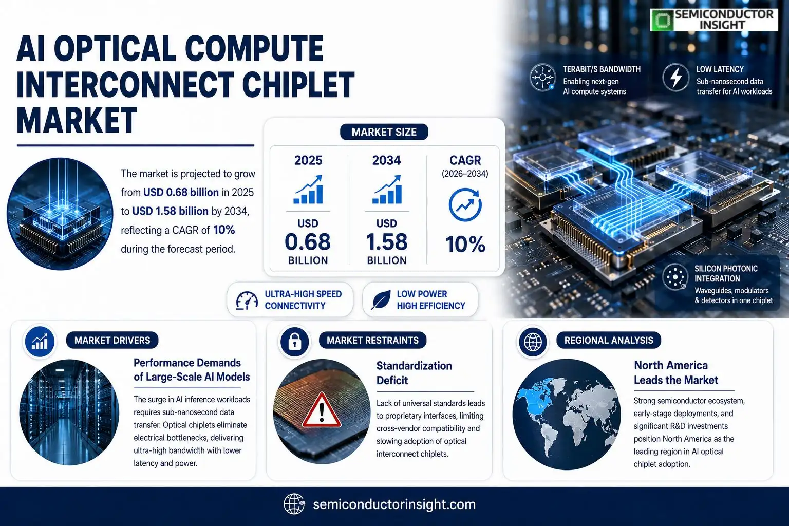
AI optical compute interconnect chiplet market size was valued at USD 0.68 billion in 2025 and will increase to USD 1.58 billion by 2034, reflecting a compound annual growth rate of roughly 10 % over the forecast horizon.
AI optical compute interconnect chiplets are modular photonic components that enable ultra‑high‑speed data exchange between AI accelerators and memory subsystems without relying on traditional electrical wiring. By integrating waveguides, modulators and detectors into a single package, these chiplets reduce latency and power consumption while supporting bandwidths beyond terabits per second.The expansion of this segment stems from mounting pressure on data‑center operators to meet ever‑growing AI inference workloads, coupled with substantial capital infusion into silicon‑photonic research by leading semiconductor firms. Recent collaborations,such as Intel’s February 2024 alliance with Lightmatter aimed at co‑developing next‑generation photonic interconnects,illustrate how ecosystem partnerships are accelerating product rollouts. Moreover, standardization efforts within the OIF (Optical Internetworking Forum) are lowering integration barriers for OEMs seeking scalable solutions.
MARKET DRIVERS
Performance Demands of Large‑Scale AI Models
Enterprises deploying generative AI are encountering latency ceilings in conventional electronic interconnects. The need for sub‑nanosecond data transfer has compelled silicon designers to embed optical pathways directly into chiplets. By eliminating electrical bottlenecks, AI Optical Compute Interconnect Chiplet Market is seeing adoption in hyperscale data centers that prioritize throughput over cost.
Energy‑Efficiency Pressures
Power budgets for AI training clusters are tightening as utility rates climb. Optical interconnects consume a fraction of the wattage required by copper links, translating into lower OPEX for operators. This efficiency advantage has persuaded several leading foundries to qualify their process nodes for photonic integration, thereby expanding the supply chain.
➤ Customers who switched to optical chiplet solutions reported up to a 30% reduction in energy per inference, reshaping total cost of ownership calculations.
The convergence of these forces has led system architects to prioritize chiplet‑level photonics when laying out next‑generation AI accelerators, creating a virtuous loop of demand for specialized design IP.
MARKET CHALLENGES
Manufacturing Yield Complexities
Integrating waveguides into densely packed silicon dies introduces new sources of defect. Yield rates for early‑generation optical chiplets hover around 70%, markedly lower than mature electronic counterparts. The gap forces OEMs to hold additional inventory, eroding the cost advantage of photonics.
Other Challenges
Design‑Tool Ecosystem Gaps
CAD suites have historically emphasized electronic routing; few provide native support for photonic layout. Engineers must cobble together disparate tools, extending time‑to‑market for new AI chips.Supply‑chain volatility for specialty glass further complicates scaling, as the material base for waveguide cores is sourced from a limited pool of manufacturers.
MARKET RESTRAINTS
Standardization Deficit
Without a universally accepted optical interconnect specification, each vendor develops proprietary interfaces. This fragmentation hampers cross‑vendor integration and discourages smaller players from entering AI Optical Compute Interconnect Chiplet Market.Regulatory scrutiny over high‑speed laser sources also introduces compliance costs. Agencies are tightening emission standards for photonic components, prompting designers to incorporate additional shielding, which inflates BOM values.
MARKET OPPORTUNITIES
Edge‑AI Deployments Requiring Compact Bandwidth Solutions
Edge servers that host inference workloads are constrained by limited form factor and thermal envelope. Embedding optical chiplets directly onto ASICs enables high‑density I/O without additional cooling infrastructure, positioning AI Optical Compute Interconnect Chiplet Market to capture a niche in on‑premise AI acceleration.Another avenue lies in hyperscale cloud providers experimenting with disaggregated architectures. By decoupling compute from memory via optical chiplets, providers can re‑configure rack layouts on the fly, unlocking new business models around compute‑as‑a‑service.
AI Optical Compute Interconnect Chiplet Market Trends
Modular Photonic Integration Fuels Adoption
AI Optical Compute Interconnect Chiplet Market is seeing increased interest as data‑center operators confront mounting AI inference demand. By embedding waveguides, modulators and detectors within a single chiplet, manufacturers are delivering ultra‑high‑speed pathways that cut both latency and power draw. Bandwidths measured in terabits per second now become feasible without the bulk of traditional electrical interconnects, allowing servers to sustain higher throughput while keeping energy budgets in check. This engineering advantage translates directly into lower total cost of ownership for operators seeking to scale AI workloads without a proportional rise in infrastructure spend.
Other Trends
Ecosystem Partnerships Accelerate Productization
Strategic alliances are reshaping the pace at which new chiplet solutions reach the market. The February 2024 collaboration between Intel and Lightmatter exemplifies how semiconductor giants and photonic specialists pool R&D resources to refine fabrication processes and accelerate validation cycles. Parallel investments from other leading firms signal confidence in silicon‑photonic platforms, prompting a surge of joint road‑maps that align product timelines with customer demand. These partnerships reduce the risk associated with early‑stage technology rollout and create clearer pathways for OEMs to adopt standardized components.
Standardization Lowers Integration Barriers
Progress within the Optical Internetworking Forum (OIF) is gradually aligning specifications for chiplet‑based interconnects, making it easier for hardware designers to embed photonic modules into existing silicon ecosystems. Uniform electrical‑to‑optical conversion rules and defined test methodologies give system architects confidence that third‑party chiplets will interoperate reliably across diverse platforms. As the reference stack matures, the engineering effort required for custom integration diminishes, encouraging a broader set of data‑center vendors to experiment with optical solutions rather than relying exclusively on legacy copper networks.
COMPETITIVE LANDSCAPEKey Industry Players
AI Optical Compute Interconnect Chiplet Market: Competitive Overview
Intel remains the anchor of the ecosystem, leveraging its extensive silicon‑photonic IP portfolio and foundry capacity to supply both standalone chiplets and integrated AI accelerator modules. The February 2024 partnership with Lightmatter underscores a strategic move toward co‑engineering photonic pathways that cut latency while preserving power budgets. Intel’s ability to bundle design‑win services with high‑volume manufacturing gives it a decisive edge in courting hyperscale data‑center operators that demand reliable, low‑cost interconnects. Lightmatter, meanwhile, contributes breakthrough silicon‑photonics designs that push per‑channel bandwidth beyond 1 Tb/s, positioning the duo as the de‑facto reference architecture for next‑generation AI clusters.Beyond the flagship collaboration, a cadre of niche innovators is shaping the market’s depth. Lumentum and II‑VI Incorporated supply high‑performance modulators and detectors that feed smaller‑form‑factor chiplet offerings. Acacia Communications, now part of Cisco, injects mature coherent‑optics technology that eases integration for OEMs targeting hybrid electrical‑photonic platforms. Rockley Photonics (under Lumentum), Ciena, and Broadcom bring differentiated packaging expertise that enables dense interposer routing. Regional players such as Nokia (through Oclaro) and Marvell (via Inphi acquisition) address telecom‑driven AI workloads, while startups like Ayar Labs and PhotonIC focus on ultra‑low‑power waveguide architectures, expanding the supply chain beyond the traditional semiconductor giants.
List of Key AI Optical Compute Interconnect Chiplet Companies Profiled
- Intel Corporation
- Lightmatter, Inc.
- Lumentum Holdings Inc.
- II‑VI Incorporated
- Acacia Communications (Cisco)
- Rockley Photonics (Lumentum)
- Ciena Corporation
- Broadcom Inc.
- Nokia (Oclaro)
- Marvell Technology Group Ltd.
- Ayar Labs
- PhotonIC
- Inphi Corporation (Marvell)
- Applied Materials, Inc.
- AMD (Xilinx)
Segment Analysis:
| Segment Category | Sub-Segments | Key Insights |
| By Type |
|
Photonic Waveguide Chiplets are emerging as the primary enabler for ultra‑high‑speed data paths. Their inherent low‑loss propagation and ability to route light across dense interconnect fabrics make them attractive for next‑generation AI accelerators.
|
| By Application |
|
Data Center Accelerators drive the most compelling use cases, where massive AI inference workloads demand minimal latency and power consumption. Optical chiplets interconnect accelerator cards and memory modules, turning bandwidth bottlenecks into opportunities for performance scaling.
|
| By End User |
|
Cloud Service Providers are rapidly adopting optical interconnect chiplets to sustain the relentless demand for AI compute capacity across shared infrastructures. Their focus on operational efficiency amplifies interest in photonic solutions that lower total cost of ownership.
|
| By Architecture |
|
Hybrid Electro‑Optical Architectures are gaining traction as they blend the maturity of electronic routing with the bandwidth advantages of photonics. This balanced approach eases transition for vendors while delivering immediate performance benefits.
|
| By Integration Approach |
|
Heterogeneous 3D Stacking emerges as the preferred method for delivering dense optical interconnects alongside electronic logic, fostering compact form factors suited for modern AI servers.
|
Regional Analysis: AI Optical Compute Interconnect Chiplet Market
North America
In the North American ecosystem, the convergence of photonic research labs and silicon‑based foundries creates a fertile ground for AI Optical Compute Interconnect Chiplet development. Major cloud providers have launched dedicated programs that invite start‑ups to prototype chiplet‑level optical links, effectively shortening the time from concept to field trial. The presence of deep‑tech venture capital firms accelerates this cycle, allowing firms to secure multi‑stage funding without prolonged series of proof‑of‑concept demos.While the United States dominates design talent, Canada and Mexico contribute niche expertise in low‑loss waveguide fabrication, fostering cross‑border collaborations that broaden the supply chain. This geographic diversity reduces reliance on any single wafer source, mitigating risks associated with capacity constraints.
Regulatory bodies have introduced targeted tax credits for photonic R&D, encouraging manufacturers to embed optical interconnects directly into AI accelerators. The resulting ecosystem not only shortens latency for data‑center workloads but also opens avenues for edge‑computing deployments where power efficiency is paramount. Collectively, these dynamics cement North America’s status as the primary incubator for the next generation of AI compute architectures.
Silicon Valley, Boston, and Austin host clusters where photonic design houses co‑locate with AI chip firms, fostering rapid prototype iteration and joint intellectual property development that fuels the chiplet ecosystem.
Established fabs in Arizona and Texas have repurposed portions of their 300‑mm lines for low‑temperature waveguide processes, delivering the volume needed for emerging chiplet volumes while preserving legacy silicon throughput.
Strategic alliances between optical component suppliers and AI accelerator designers create standardized link specifications, simplifying integration and reducing time‑to‑market for new chiplet packages.
Federal and state programs award credits for photonic R&D, encouraging firms to locate design teams near research universities that specialize in nanophotonic physics.
Europe
European research consortia have placed photonic integration at the core of their AI hardware roadmaps, leveraging the continent’s strong tradition in precision optics. Countries such as Germany and the Netherlands combine mature lithography infrastructure with a deep pool of optical engineering talent, allowing them to produce chiplet‑ready optical waveguides at a competitive cost. Collaborative grants from the European Commission stimulate joint ventures between semiconductor manufacturers and AI firms, ensuring that design standards evolve in step with market needs. The region’s emphasis on sustainability also drives the adoption of energy‑efficient optical links, positioning Europe as a credible challenger in the supply chain.
Asia‑Pacific
Asia‑Pacific delivers a blend of scale and cost discipline that reshapes AI Optical Compute Interconnect Chiplet Market’s cost‑structure. Taiwan’s foundry ecosystem, supported by decades of advanced silicon processing, now extends its capabilities into silicon‑photonic node development, offering manufacturers a single‑source solution for both logic and optical layers. Meanwhile, Japan’s expertise in low‑loss polymer waveguides feeds niche high‑performance applications, particularly in autonomous vehicle platforms. Regional governments provide subsidies aimed at accelerating photonic talent pipelines, creating a talent bridge that links university research to commercial chiplet design houses. The combination of manufacturing depth and policy support sustains rapid design turnover across the region.
South America
South America is gradually emerging as a testbed for edge‑centric AI workloads that benefit from compact optical interconnects. Brazil’s growing semiconductor ecosystem, bolstered by government‑backed innovation hubs, focuses on integrating chiplet‑based optical links into locally‑manufactured AI accelerators for agricultural IoT devices. While volume production remains limited, partnerships with North American fab services allow local firms to prototype designs without heavy capital outlay. The regional emphasis on cost‑sensitive applications drives a pragmatic approach: designers prioritize modularity and ease of assembly, laying groundwork for future expansion as supply‑chain confidence improves.
Middle East & Africa
In the Middle East & Africa, nascent photonic initiatives are anchored by sovereign wealth funds that allocate capital toward high‑tech diversification. United Arab Emirates and Saudi Arabia have launched research parks that attract photonic equipment providers, fostering knowledge transfer to local engineering teams. Although the market remains early‑stage, the emphasis on data‑center expansion to support burgeoning cloud services creates a clear demand signal for energy‑efficient optical chiplet solutions. Collaborative projects with European universities inject design expertise, while regional telecom operators experiment with chiplet‑enabled optical switches to improve network latency for AI‑driven services. The trajectory suggests a slow but steady climb toward a more substantive market presence.
Report Scope
This market research report provides a comprehensive analysis of the AI Optical Compute Interconnect Chiplet Market , covering the forecast period 2026–2034. It offers detailed insights into market dynamics, technological advancements, competitive landscape, and key trends shaping the industry.
Key focus areas of the report include:
- Market Overview: The report begins with an overview outlining its current market scenario, key growth indicators, and industry transformation drivers. It discusses macroeconomic factors, demand–supply balance, regulatory landscape, and the strategic role of semiconductors in powering advancements across industries such as automotive, telecommunications, consumer electronics, and industrial automation.
- Market Size & Forecast: Historical data and future projections for revenue, unit shipments, and market value across major regions and segments.
- Segmentation Analysis: Detailed breakdown by product type, technology, application, and end-user industry to identify high-growth segments and investment opportunities.
- Regional Insights: Insights into market performance across North America, Europe, Asia-Pacific, Latin America, and the Middle East & Africa, including country-level analysis where relevant.
- Competitive Landscape: Profiles of leading market participants, including their product offerings, R&D focus, manufacturing capacity, pricing strategies, and recent developments such as mergers, acquisitions, and partnerships.
- Technology Trends & Innovation: Assessment of emerging technologies, integration of AI/IoT, semiconductor design trends, fabrication techniques, and evolving industry standards.
- Market Drivers & Restraints: Evaluation of factors driving market growth along with challenges, supply chain constraints, regulatory issues, and market-entry barriers.
- Stakeholder Insights: Insights for component suppliers, OEMs, system integrators, investors, and policymakers regarding the evolving ecosystem and strategic opportunities.
Primary and secondary research methods are employed, including interviews with industry experts, data from verified sources, and real-time market intelligence to ensure the accuracy and reliability of the insights presented.
FREQUENTLY ASKED QUESTIONS:
What is the current market size of AI Optical Compute Interconnect Chiplet Market?
-> AI Optical Compute Interconnect Chiplet Market was valued at USD 0.68 billion in 2025 and is expected to reach USD 1.58 billion by 2034, reflecting a compound annual growth rate of roughly 10 %.
Which key companies operate in AI Optical Compute Interconnect Chiplet Market?
-> Key players include Intel Corporation, Lightmatter, Lumentum Holdings, Cisco Systems, and Acacia Communications, among others.
What are the key growth drivers?
-> Key growth drivers include rising AI inference workloads in data centers, demand for ultra‑high‑speed low‑latency interconnects, power‑efficiency requirements, and increasing capital investment in silicon‑photonic research.
Which region dominates the market?
-> Asia-Pacific is emerging as the fastest‑growing region, while North America remains a dominant market due to strong semiconductor ecosystem and early‑stage deployments.
What are the emerging trends?
-> Emerging trends include standardization efforts by the Optical Internetworking Forum (OIF), integration of AI‑accelerator chiplets with photonic interconnects, and co‑development partnerships between fabless and foundry players.
Get Sample Report PDF for Exclusive Insights
Report Sample Includes
- Table of Contents
- List of Tables & Figures
- Charts, Research Methodology, and more...
 Download Sample Report PDF