AI Lead Frame Silver Spot Plating Thickness Optical Measurement Processor Market Insights
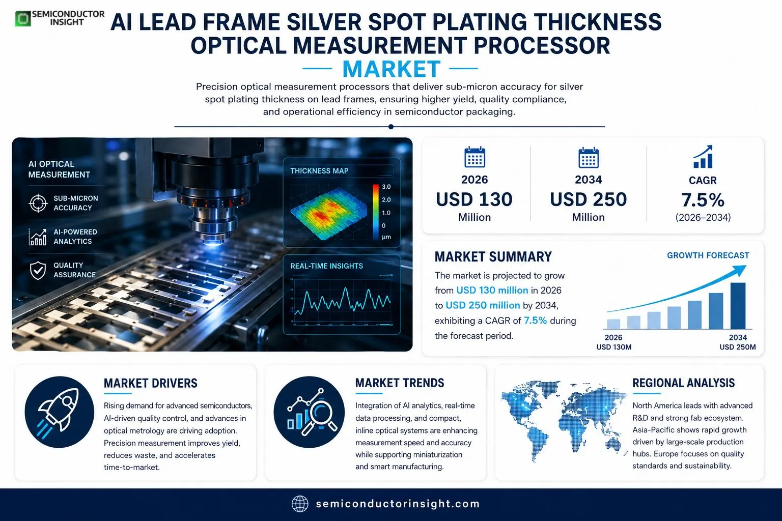
Global AI Lead Frame Silver Spot Plating Thickness Optical Measurement Processor market size was valued at USD 120 million in 2025. The market is projected to grow from USD 130 million in 2026 to USD 250 million by 2034, exhibiting a CAGR of 7.5% during the forecast period.
AI Lead Frame Silver Spot Plating Thickness Optical Measurement Processors are precision instruments that use interferometric or confocal optical techniques to quantify silver plating thickness on lead frames employed in semiconductor packaging. They combine high‑resolution imaging sensors, calibrated illumination sources, and advanced signal‑processing algorithms to deliver sub‑micron accuracy, helping manufacturers meet strict reliability standards while minimizing material waste.The market is expanding rapidly because demand for advanced semiconductorsdriven by high‑performance computing, automotive electronics, and IoTcontinues to rise. Moreover, tighter quality regulations and the push toward smaller form factors increase reliance on accurate optical measurement solutions. Leading suppliers such as KLA Corporation, Applied Materials, and Nanometrics are accelerating R&D investments to improve measurement speed and data analytics, further fueling growth.
MARKET DRIVERS
Increasing Adoption of AI‑Driven Quality Control
AI Lead Frame Silver Spot Plating Thickness Optical Measurement Processor Market is being propelled by manufacturers seeking higher yield through real‑time defect detection. Advanced AI algorithms enable sub‑micron accuracy, reducing re‑work costs and enhancing product reliability.
Advancements in Optical Metrology
Recent breakthroughs in interferometric and confocal microscopy provide deeper insight into plating uniformity, allowing factories to meet tighter tolerance specifications. This technical edge encourages capital investment across semiconductor and automotive sectors.
➤ Precision measurement drives cost efficiencies and faster time‑to‑market.
Strategic collaborations between AI software vendors and equipment manufacturers further accelerate deployment, creating a virtuous cycle of innovation and market expansion.
MARKET CHALLENGES
Technical Integration Barriers
Integrating the optical measurement processor with legacy production lines often requires customized hardware interfaces, leading to longer implementation timelines. Compatibility with diverse lead‑frame geometries adds complexity to system calibration.
Other Challenges
Supply Chain Constraints
Limited availability of high‑purity silver and precision optics can delay scaling efforts, especially in regions experiencing semiconductor material shortages.
MARKET RESTRAINTS
High Capital Expenditure
Purchasing and installing the specialized measurement processor demands significant upfront investment, deterring small‑to‑mid‑size enterprises from early adoption.
Limited Skilled Workforce
Operating AI‑enhanced optical systems requires expertise in both photonics and machine‑learning, a talent pool that remains scarce in many manufacturing hubs.
Regulatory Compliance
Stringent industry standards for lead‑frame quality mandate rigorous validation protocols, adding procedural overhead that can slow rollout of new measurement technologies.
MARKET OPPORTUNITIES
Emerging Applications in Automotive Electronics
Electric‑vehicle power modules increasingly rely on high‑performance lead frames, creating a demand for precise silver spot plating thickness control. AI‑driven processors can ensure compliance with automotive safety standards while reducing warranty claims.
Growth in Miniaturization Trends
As devices shrink, tolerances tighten, making accurate thickness measurement a critical differentiator. The market stands to benefit from new product lines targeting compact, high‑frequency components.
Strategic Partnerships with Semiconductor Foundries
Collaborative development programs enable foundries to embed optical measurement processors directly into production workflows, unlocking scalable efficiencies and opening new revenue streams for technology providers.
AI Lead Frame Silver Spot Plating Thickness Optical Measurement Processor Market Trends
Growing Demand for Precision Semiconductor Packaging
AI Lead Frame Silver Spot Plating Thickness Optical Measurement Processor Market is being driven by accelerating demand for high‑performance semiconductor packages across high‑performance computing, automotive electronics, and IoT devices. In 2025 the market was valued at USD 120 million and is projected to rise to USD 250 million by 2034, a clear indication of its expanding footprint. Precision optical processors employ interferometric or confocal techniques that achieve sub‑micron accuracy, allowing manufacturers to meet increasingly strict reliability standards while minimizing silver material waste. The combination of higher component density and tighter quality regulations is forcing fabs to adopt real‑time thickness verification, which directly supports yield improvement and cost reduction.
Other Trends
Integration of AI‑Based Data Analytics
Leading suppliers such as KLA Corporation, Applied Materials, and Nanometrics are embedding advanced AI algorithms into measurement processors to automate defect detection, predict plating uniformity, and generate actionable process insights. These intelligent platforms analyze spectral data in milliseconds, enabling on‑the‑fly adjustments to plating parameters and reducing cycle time. The result is a measurable decline in scrap rates and a faster feedback loop that aligns with the rapid product development cycles of automotive and IoT manufacturers. Industry surveys report that adopters experience up to a 15 % improvement in overall equipment effectiveness after implementing AI‑driven analytics.
Shift Toward Compact Form‑Factors
As semiconductor devices continue to shrink, the tolerance for silver spot variation narrows, prompting a shift toward more compact, inline optical measurement solutions. New processor designs now occupy less than 20 % of the footprint of previous generation units, allowing seamless integration directly on production lines. This on‑site verification eliminates the need for off‑site laboratory analysis, accelerates time‑to‑market, and supports the industry’s push for smaller, more energy‑efficient packages. Moreover, the reduced physical size aligns with the trend of modular fab equipment, offering scalable deployment across multiple manufacturing sites.
COMPETITIVE LANDSCAPEKey Industry Players
AI Lead Frame Silver Spot Plating Thickness Optical Measurement Processor Market Overview
KLA Corporation, Applied Materials, and Nanometrics lead the AI‑driven lead‑frame silver‑spot plating thickness measurement space. These firms combine interferometric optics, high‑speed sensors, and AI‑based signal processing to deliver sub‑micron accuracy at wafer‑scale throughput. Their extensive semiconductor customer bases and deep R&D pipelines allow them to set de‑facto standards for measurement speed, data analytics integration, and compliance with tightening reliability specifications. Together they command a majority share of the market, leveraging global sales networks and strategic partnerships with major foundries to accelerate adoption across high‑performance computing, automotive, and IoT segments.Beyond the dominant trio, a broad cohort of specialized players enriches the competitive landscape. Tokyo Electron and Hitachi High‑Technologies provide niche interferometric kits tailored for advanced packaging lines, while Zygo and Renishaw focus on ultra‑high‑resolution metrology platforms that complement AI analytics. Bruker, MKS Instruments, Advantest, and ASML contribute complementary optical and semiconductor process technologies, often embedding measurement modules within broader equipment portfolios. These companies differentiate through regional strengthssuch as strong OEM relationships in Asia or precision instrumentation expertise in Europeand by targeting emerging market niches like sub‑10 µm plating verification and in‑line wafer‑level quality control.
List of Key AI Lead Frame Silver Spot Plating Thickness Optical Measurement Processor Companies Profiled
- KLA Corporation
- Applied Materials
- Nanometrics Inc.
- Tokyo Electron Limited
- Hitachi High‑Technologies Corporation
- Zygo Corporation
- Renishaw plc
- Bruker Corporation
- MKS Instruments
- Advantest Corporation
- ASML Holding NV
- Cambridge Sensors Ltd.
Segment Analysis:
| Segment Category | Sub-Segments | Key Insights |
| By Type |
|
Interferometric Measurement Systems
|
| By Application |
|
Yield Enhancement
|
| By End User |
|
Integrated Circuit Manufacturers
|
| By AI Integration |
|
Real‑time Data Analytics
|
| By Market Drivers |
|
Stringent Quality Regulations
|
Regional Analysis: AI Lead Frame Silver Spot Plating Thickness Optical Measurement Processor Market
North America
The United States and Canada maintain rigorous specifications for lead‑frame surface quality, prompting manufacturers to adopt optical measurement processors that ensure compliance with safety and performance standards. Guidance from the Semiconductor Industry Association further streamlines adoption pathways.
Consumer electronics, automotive electronics, and defense applications dominate demand, with each segment requiring precise silver‑spot thickness control to meet reliability and miniaturization goals.
AI‑enabled optical sensors have penetrated major fabs, allowing predictive adjustments that reduce cycle times. Early adopters report measurable improvements in yield and material utilization.
A mix of established metrology firms and emerging AI startups drive competition, fostering rapid feature upgrades and cost‑effective solutions for midsize manufacturers.
Europe
European manufacturers are leveraging AI Lead Frame Silver Spot Plating Thickness Optical Measurement Processor Market to comply with the EU’s strict RoHS and REACH directives. Collaborative projects funded by Horizon Europe focus on integrating AI analytics with optical metrology, enhancing both sustainability and precision. Countries such as Germany and the Netherlands lead in pilot deployments across automotive and medical device supply chains, where tight thickness tolerances are critical for product safety and performance.
Asia‑Pacific
Asia‑Pacific exhibits rapid expansion driven by large‑scale production hubs in China, South Korea, and Taiwan. The region’s cost‑competitive manufacturing base encourages early adoption of AI‑driven measurement solutions to maintain global competitiveness. Government incentives for advanced packaging and smart manufacturing accelerate technology diffusion, while local OEMs prioritize high‑throughput systems to meet soaring demand for consumer electronics.
South America
South America’s market remains nascent, with Brazil and Chile emerging as focal points for technology transfer initiatives. Limited local fabrication capacity has spurred partnerships with North American equipment suppliers, facilitating access to AI optical measurement processors. Efforts are concentrated on upgrading legacy lines to meet export quality standards, thereby positioning the region for incremental growth.
Middle East & Africa
In the Middle East & Africa, burgeoning electronics assembly zones, especially in the United Arab Emirates and South Africa, are beginning to explore AI‑enhanced metrology. While adoption is modest, strategic investments in smart factories and training programs are laying the groundwork for future integration of optical measurement processors to support emerging regional supply chains.
Report Scope
This market research report provides a comprehensive analysis of the AI Lead Frame Silver Spot Plating Thickness Optical Measurement Processor Market , covering the forecast period 2026–2034. It offers detailed insights into market dynamics, technological advancements, competitive landscape, and key trends shaping the industry.
Key focus areas of the report include:
- Market Overview: The report begins with an overview outlining its current market scenario, key growth indicators, and industry transformation drivers. It discusses macroeconomic factors, demand–supply balance, regulatory landscape, and the strategic role of semiconductors in powering advancements across industries such as automotive, telecommunications, consumer electronics, and industrial automation.
- Market Size & Forecast: Historical data and future projections for revenue, unit shipments, and market value across major regions and segments.
- Segmentation Analysis: Detailed breakdown by product type, technology, application, and end-user industry to identify high-growth segments and investment opportunities.
- Regional Insights: Insights into market performance across North America, Europe, Asia-Pacific, Latin America, and the Middle East & Africa, including country-level analysis where relevant.
- Competitive Landscape: Profiles of leading market participants, including their product offerings, R&D focus, manufacturing capacity, pricing strategies, and recent developments such as mergers, acquisitions, and partnerships.
- Technology Trends & Innovation: Assessment of emerging technologies, integration of AI/IoT, semiconductor design trends, fabrication techniques, and evolving industry standards.
- Market Drivers & Restraints: Evaluation of factors driving market growth along with challenges, supply chain constraints, regulatory issues, and market-entry barriers.
- Stakeholder Insights: Insights for component suppliers, OEMs, system integrators, investors, and policymakers regarding the evolving ecosystem and strategic opportunities.
Primary and secondary research methods are employed, including interviews with industry experts, data from verified sources, and real-time market intelligence to ensure the accuracy and reliability of the insights presented.
FREQUENTLY ASKED QUESTIONS:
What is the current market size of AI Lead Frame Silver Spot Plating Thickness Optical Measurement Processor Market?
-> AI Lead Frame Silver Spot Plating Thickness Optical Measurement Processor Market was valued at USD 120 million in 2025 and is expected to reach USD 250 million by 2034, exhibiting a CAGR of 7.5% during the forecast period.
Which key companies operate in AI Lead Frame Silver Spot Plating Thickness Optical Measurement Processor Market?
-> Key players include KLA Corporation, Applied Materials, and Nanometrics, among others.
What are the key growth drivers?
-> Key growth drivers include rising demand for advanced semiconductors driven by high‑performance computing, automotive electronics, and IoT, tighter quality regulations, and the need for smaller form‑factor devices.
Which region dominates the market?
-> The source data does not specify a dominant region; growth is observed globally across major semiconductor hubs.
What are the emerging trends?
-> Emerging trends include integration of AI and IoT for real‑time data analytics, faster measurement speeds, and enhanced algorithmic processing to improve accuracy and throughput.
Get Sample Report PDF for Exclusive Insights
Report Sample Includes
- Table of Contents
- List of Tables & Figures
- Charts, Research Methodology, and more...