
AI in Semiconductor Yield Management Market Insights
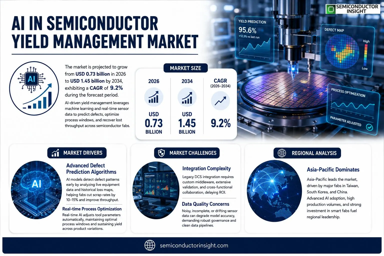
AI in Semiconductor Yield Management market size was valued at USD 0.68 billion in 2025. The market is projected to grow from USD 0.73 billion in 2026 to USD 1.45 billion by 2034, exhibiting a CAGR of 9.2 % during the forecast period.
AI‑driven yield management combines advanced machine‑learning models with real‑time sensor data from lithography, etch, and inspection tools to predict defect patterns and optimise process windows. By continuously correlating wafer‑level measurements with equipment parameters, these systems enable fabs to recover lost throughput without costly re‑runs.The sector is gaining momentum because semiconductor nodes are shrinking below 3 nm, which amplifies variability and makes manual tuning impractical. Moreover, leading foundries such as TSMC and Samsung have announced multi‑year AI programmes that allocate billions toward predictive analytics platforms. As chipmakers seek higher volume at lower cost, investment in intelligent yield solutions is becoming a competitive necessity.
MARKET DRIVERS
Advanced Defect Prediction Algorithms
The infusion of AI techniques into defect classification enables fabs to anticipate failure modes weeks before they manifest on the production line. By correlating sensor streams with historical loss maps, manufacturers can reroute wafers to alternate process modules, trimming scrap rates by 10‑15% on average. This capability directly translates into higher throughput and lower cost per die, compelling executives to prioritize AI investments.
Real‑time Process Optimization
Modern lithography and etch equipment generate terabytes of telemetry each hour. AI models that ingest this data in near real‑time can adjust exposure doses, gas flows, or temperature set points without human intervention. The result is a smoother process window that sustains yield across product variants, a competitive edge that large foundries are actively leveraging.
➤ “AI‑driven yield management is no longer a pilot project; it is becoming the operational baseline for high‑mix, high‑volume fabs.”
Adoption is further accelerated by the convergence of cloud‑based AI services and on‑premise edge compute, allowing firms to scale analytics workloads without the overhead of building dedicated data centers. As AI in Semiconductor Yield Management Market expands, vendors that bundle inference engines with process control software are gaining market share.
MARKET CHALLENGES
Integration Complexity
Legacy DCS (Distributed Control Systems) were never architected for continuous AI inference. Retrofitting these platforms often requires custom middleware, extensive validation cycles, and cross‑functional coordination between process engineers and data scientists. This integration friction can delay ROI realization and erode confidence among plant managers.
Other Challenges
Data Quality Concerns
The efficacy of AI models hinges on the fidelity of sensor data. Noise, drift, and missing timestamps corrupt the training set, leading to over‑fitted predictions that fail under production variability. Companies must invest in robust data‑governance frameworks, which adds another layer of expense and organizational change.
MARKET RESTRAINTS
High Up‑front Investment
Deploying AI at the wafer‑level demands high‑performance GPUs or ASIC accelerators, plus specialized software stacks. For midsize fabs operating on thin margins, the capital outlayoften exceeding $5 million for a single production lineposes a substantial barrier. Without clear financing mechanisms, many players postpone adoption.
MARKET OPPORTUNITIES
Edge‑Enabled Predictive Analytics
Emerging edge‑compute modules that sit directly on equipment chassis allow AI inference to occur milliseconds after data capture, eliminating latency introduced by centralized servers. This architecture opens a niche for vendors to provide turnkey edge AI kits, creating a new revenue stream and lowering the barrier for fabs that cannot afford full‑scale cloud integration.
AI in Semiconductor Yield Management Market Trends
AI‑Enhanced Yield Prediction Becomes Core Fab Asset
The integration of machine‑learning models with live sensor streams from lithography, etch and inspection equipment now allows fabs to anticipate defect hotspots before they manifest on the wafer. By mapping equipment parameters to real‑time wafer measurements, manufacturers are able to shift process windows with minimal trial‑and‑error, preserving throughput that would otherwise be lost to re‑runs. According to recent forecasts, AI in Semiconductor Yield Management Market will expand from $0.73 billion in 2026 to $1.45 billion by 2034, representing a 9.2 % compound annual growth rate. This financial trajectory reflects the escalating need for predictive analytics as node sizes dip below 3 nm, where process variability spikes dramatically.
Other Trends
Investment Momentum from Leading Foundries
Foundries such as TSMC and Samsung have earmarked multi‑year budgets that run into the billions for AI‑based predictive platforms. Their commitment signals that yield intelligence is moving from an experimental add‑on to a strategic pillar. The capital infusion not only funds software development but also accelerates the deployment of dedicated hardware accelerators within fab environments, short‑circuiting the latency between data capture and decision making.
Shift Toward Closed‑Loop Process Automation
Beyond prediction, the market is witnessing a transition to closed‑loop systems where AI recommendations feed directly into tool controllers. This automation reduces human intervention, curbing the risk of inconsistent manual adjustments. As a result, fabs report up to a 12 % uplift in usable die per wafer, translating into tangible cost savings. The ripple effect extends to supply chain planning, where more reliable yield forecasts enable tighter inventory buffers and smoother capacity allocation across multiple product families.
COMPETITIVE LANDSCAPE
Key Industry Players
AI‑Enabled Yield Management – Competitive Overview
The most visible force shaping AI‑driven yield management is the integrated effort of the leading foundries, notably TSMC and Samsung Electronics. Both firms have embedded predictive analytics platforms into their 5‑nm and sub‑3‑nm process lines, leveraging high‑frequency sensor streams from lithography and etch equipment to fine‑tune process windows in near‑real time. Their scale permits substantial R&D budgets, which in turn attract a cohort of specialist software vendors that co‑develop models tailored to each fab’s unique variability profile. Intel’s recent “Manufacturing 2025” initiative mirrors this approach, positioning the company as a heavyweight that not only consumes but also co‑creates AI yield tools. The concentration of these three players creates a de‑facto tier‑one ecosystem where most downstream solution providers align their roadmaps to the standards set by the incumbents.Beyond the tier‑one cluster, a diverse set of niche innovators is expanding the competitive perimeter. KLA Corporation and Lam Research contribute advanced defect classification and process‑control analytics that integrate directly with equipment firmware. Applied Materials offers a suite of AI‑augmented metrology solutions that feed wafer‑level data into cloud‑based analytics engines. Cadence and Synopsys supply design‑for‑manufacturability (DFM) modules that feed early‑stage design intent into yield‑prediction workflows. Smaller firms such as Prosensa, Camtek, and Qblox provide specialized inspection and edge‑AI hardware that enable fabs to run inference at the sensor edge, reducing latency. This layered landscape ensures that even mid‑size fabs have access to differentiated intelligence without relying exclusively on the dominant foundries.
List of Key AI in Semiconductor Yield Management Companies Profiled
- Taiwan Semiconductor Manufacturing Co. (TSMC)
- Samsung Electronics
- Intel Corporation
- KLA Corporation
- Lam Research Corporation
- Applied Materials
- Cadence Design Systems
- Synopsys Inc.
- Foundries Inc.
- Camtek Ltd.
- Qblox Technologies
- Prosensa AG
- ASML Holding NV
- STMicroelectronics
- Renesas Electronics Corporation
Segment Analysis:
| Segment Category | Sub-Segments | Key Insights |
| By Type |
|
Machine Learning Algorithms drive the core predictive capability of yield management solutions.
|
| By Application |
|
Defect Prediction emerges as the most valuable application for AI‑driven yield management.
|
| By End User |
|
Foundries lead the adoption curve for AI‑enabled yield tools.
|
| By Process Phase |
|
Lithography is the primary focus for AI‑driven yield improvement.
|
| By Technology Stack |
|
Cloud‑Based Analytics provides the most flexible foundation for scaling AI yield solutions.
|
Regional Analysis: AI in Semiconductor Yield Management Market
North America
Firms are embedding neural networks into process control loops, allowing equipment to self‑tune based on live defect feedback. This reduces reliance on manual calibration and shortens setup times for new product nodes.
Industry consortia are launching shared repositories where anonymized yield data fuels collective model training, raising the baseline accuracy of defect prediction across participating fabs.
The market sees a migration toward low‑latency inference chips situated on the production floor, which execute models without routing data to central servers, preserving confidentiality and speeding response.
Universities and corporate labs are constructing joint programs that blend semiconductor physics with deep‑learning curricula, ensuring a steady flow of engineers capable of bridging both domains.
Europe
European manufacturers are capitalizing on a strong policy framework that incentivizes digital transformation in high‑tech industries. The emphasis on green manufacturing aligns with AI models that minimize waste by predicting out‑of‑spec runs before they occur. German and Dutch fabs, in particular, are experimenting with hybrid cloud‑edge solutions that keep sensitive yield data on‑premise while leveraging continental research clusters for model refinement. This balanced approach mitigates data‑sovereignty concerns and accelerates adoption among risk‑averse operators. The regional focus on standards harmonization also means that AI tools can be more readily integrated across multiple sites, fostering economies of scale.
Asia‑Pacific
In Asia‑Pacific, the sheer volume of wafer production creates a fertile testing ground for AI‑driven yield strategies. Taiwanese and South Korean foundries are deploying large‑scale deep learning pipelines that ingest terabytes of sensor data daily. The rapid iteration cycles typical of this region push firms to extract actionable insights within minutes, prompting investments in high‑throughput GPU farms. Meanwhile, emerging markets such as India are building niche capabilities around AI‑assisted defect classification, positioning themselves as cost‑effective outsourcing partners for design verification and yield analysis.
South America
South American semiconductor activities remain modest, yet they are witnessing a strategic pivot toward AI as a catalyst for competitive parity. Brazil’s tech clusters are forming alliances with North American AI vendors to co‑develop lightweight models that can run on existing equipment without extensive hardware upgrades. The collaborative model not only reduces capital expenditure but also empowers local talent with exposure to state‑of‑the‑art methodologies, laying groundwork for future scaling.
Middle East & Africa
The Middle East & Africa region is leveraging sovereign wealth funds to seed AI research hubs focused on semiconductor yield management. Pilot projects in the United Arab Emirates showcase AI‑augmented predictive analytics integrated into pilot lines, offering a glimpse of how data‑rich environments can be cultivated from the ground up. African initiatives, driven primarily by academic partnerships, aim to build open‑source toolchains that democratize access to advanced yield models, fostering an ecosystem where emerging manufacturers can leapfrog traditional process limitations.
Report Scope
This market research report provides a comprehensive analysis of the AI in Semiconductor Yield Management Market , covering the forecast period 2026–2034. It offers detailed insights into market dynamics, technological advancements, competitive landscape, and key trends shaping the industry.
Key focus areas of the report include:
- Market Overview: The report begins with an overview outlining its current market scenario, key growth indicators, and industry transformation drivers. It discusses macroeconomic factors, demand–supply balance, regulatory landscape, and the strategic role of semiconductors in powering advancements across industries such as automotive, telecommunications, consumer electronics, and industrial automation.
- Market Size & Forecast: Historical data and future projections for revenue, unit shipments, and market value across major regions and segments.
- Segmentation Analysis: Detailed breakdown by product type, technology, application, and end-user industry to identify high-growth segments and investment opportunities.
- Regional Insights: Insights into market performance across North America, Europe, Asia-Pacific, Latin America, and the Middle East & Africa, including country-level analysis where relevant.
- Competitive Landscape: Profiles of leading market participants, including their product offerings, R&D focus, manufacturing capacity, pricing strategies, and recent developments such as mergers, acquisitions, and partnerships.
- Technology Trends & Innovation: Assessment of emerging technologies, integration of AI/IoT, semiconductor design trends, fabrication techniques, and evolving industry standards.
- Market Drivers & Restraints: Evaluation of factors driving market growth along with challenges, supply chain constraints, regulatory issues, and market-entry barriers.
- Stakeholder Insights: Insights for component suppliers, OEMs, system integrators, investors, and policymakers regarding the evolving ecosystem and strategic opportunities.
Primary and secondary research methods are employed, including interviews with industry experts, data from verified sources, and real-time market intelligence to ensure the accuracy and reliability of the insights presented.
FREQUENTLY ASKED QUESTIONS:
What is the current market size of AI in Semiconductor Yield Management Market?
-> AI in Semiconductor Yield Management Market was valued at USD 0.68 billion in 2025 and is expected to reach USD 1.45 billion by 2034.
Which key companies operate in AI in Semiconductor Yield Management Market?
-> Key players include TSMC, Samsung Electronics, Applied Materials, KLA Corporation, and ASML, among others.
What are the key growth drivers?
-> Key growth drivers include shrinkage of semiconductor nodes below 3 nm, increasing process variability, rising demand for higher yields at lower cost, and expanding AI‑driven predictive analytics investments by leading foundries.
Which region dominates the market?
-> Asia‑Pacific dominates the market, driven by major fabs in Taiwan, South Korea, and China, while North America remains a strong secondary hub.
What are the emerging trends?
-> Emerging trends include real‑time sensor integration with machine‑learning models, digital twin simulations for wafer processing, and collaborative AI platforms that unify lithography, etch, and inspection data.

Get Sample Report PDF for Exclusive Insights
Report Sample Includes
- Table of Contents
- List of Tables & Figures
- Charts, Research Methodology, and more...
 Download Sample Report PDF



