
AI for Semiconductor Design for Manufacturability Market Insights
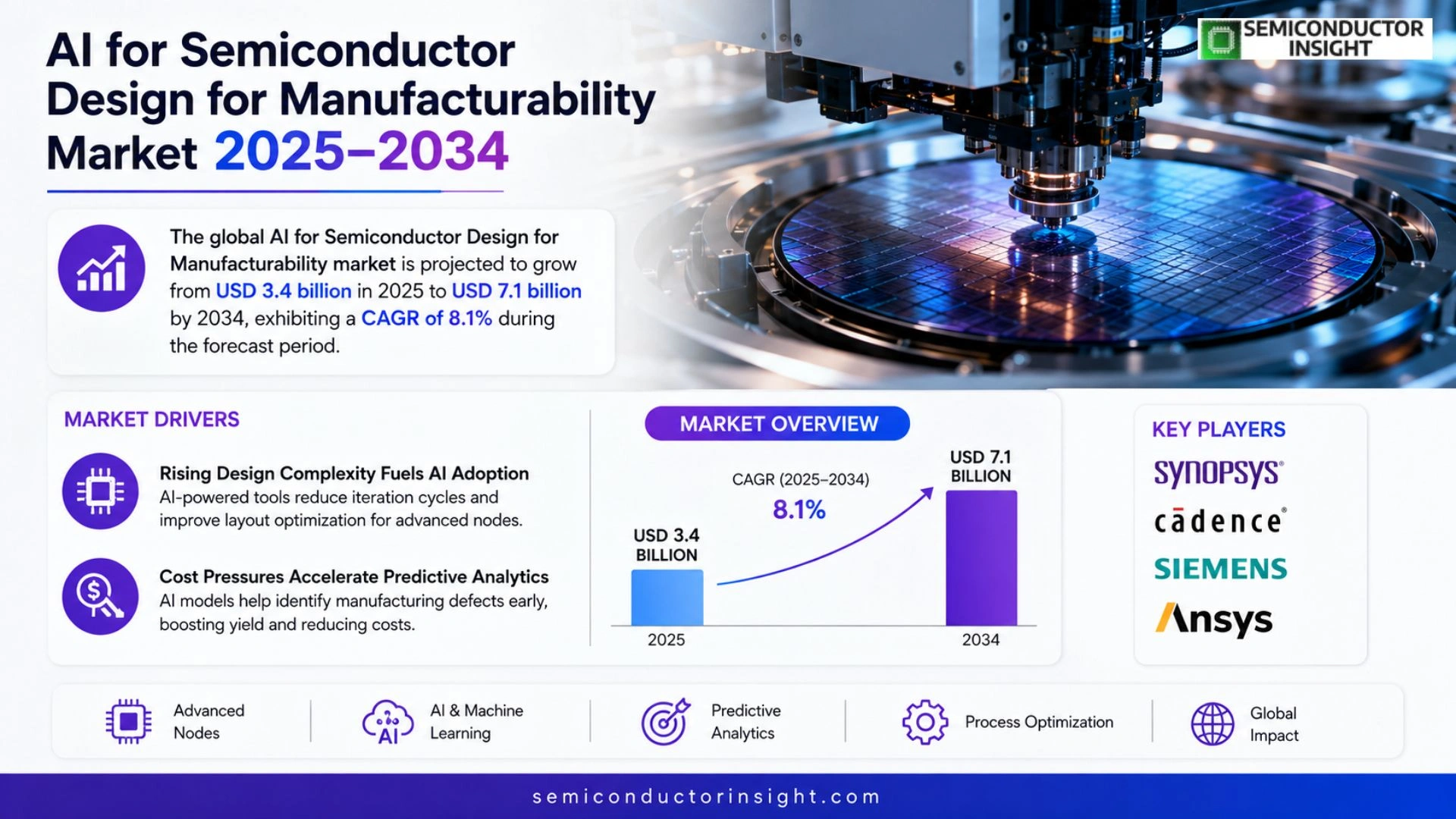
Global AI for Semiconductor Design for Manufacturability market size was valued at USD 3.2 billion in 2025. The market is projected to grow from USD 3.4 billion in 2025 to USD 7.1 billion by 2034, exhibiting a CAGR of 8.1% during the forecast period.
AI‑driven design tools enable semiconductor manufacturers to optimize layout, reduce mask iterations, and improve yield through predictive modeling and generative design techniques. These solutions integrate machine‑learning algorithms with electronic design automation (EDA) platforms, allowing designers to assess manufacturability constraints early in the chip development cycle.
The market is experiencing rapid growth due to heightened investment in advanced‑node development, escalating demand for high‑performance computing chips, and pressure to shorten time‑to‑market. Furthermore, collaborations between leading EDA vendors and AI specialists are accelerating adoption, while major foundries such as TSMC and Samsung are incorporating AI analytics into their process flows.
MARKET DRIVERS
Rising Design Complexity Fuels AI Adoption
The ongoing migration toward sub‑10 nm nodes introduces geometric constraints that traditional design tools struggle to resolve. AI for Semiconductor Design for Manufacturability Market participants report that machine‑learning‑enhanced layout engines can cut iteration cycles by nearly 40 %, allowing designers to explore a broader solution space without inflating schedule risk.
Cost Pressures Accelerate Predictive Analytics
Foundries are confronting wafer‑level yield volatility that directly impacts gross margins. Predictive defect‑detection models, a core offering within AI for Semiconductor Design for Manufacturability Market, have enabled early-stage identification of lithography hot spots, saving an estimated $200 million annually for a leading 300 mm fab.
➤ “Integrating AI into the design‑for‑manufacturability workflow has shifted our ROI horizon from years to months,” notes a senior VP of engineering at a top‑tier consumer‑electronics supplier.
Beyond immediate efficiencies, the strategic advantage of embedding manufacturability insight earlier in the RTL‑to‑GDSII flow is reshaping product roadmaps. Companies that lock in AI‑driven verification now position themselves to meet tighter time‑to‑market windows demanded by emerging IoT and automotive applications.
MARKET CHALLENGES
Data Scarcity Limits Model Generalization
Training robust AI models requires extensive defect and process data, yet many fabs restrict data sharing due to IP concerns. This limitation hampers the ability of vendors in AI for Semiconductor Design for Manufacturability Market to deliver universally applicable solutions, prompting customers to invest in bespoke data pipelines.
Other Challenges
Integration Overhead
Adapting legacy EDA environments to accommodate AI modules often incurs additional licensing fees and steep learning curves for design staff, slowing adoption rates despite clear performance benefits.
Furthermore, the lack of standardized metrics for AI‑enhanced manufacturability creates ambiguity when benchmarking vendor claims, compelling end‑users to conduct extensive pilot studies before scaling deployments.
MARKET RESTRAINTS
Regulatory and Security Concerns
Government‑mandated export controls on advanced semiconductor technologies extend to AI algorithms that influence yield. Companies operating across multiple jurisdictions must navigate a complex compliance matrix, which can delay product rollouts and increase legal overhead.
In parallel, cybersecurity threats targeting design data repositories raise doubts about the safety of cloud‑based AI services. Enterprises therefore favor on‑premise deployments, a choice that raises total cost of ownership and may deter smaller players from entering AI for Semiconductor Design for Manufacturability Market.
MARKET OPPORTUNITIES
Edge‑AI Integration for Real‑Time Yield Feedback
Embedding lightweight inference engines directly into fab equipment enables instantaneous defect classification, turning each wafer pass into a data point for continuous model refinement. This capability opens a revenue stream for AI vendors that can certify edge‑compatible runtimes.
Another avenue lies in cross‑domain collaborations between AI firms and material‑science startups. By fusing process‑level simulations with design‑centric AI, new predictive layers can anticipate variability before mask generation, effectively lowering the cost of redesign cycles.
Finally, the emergence of open‑source model repositories provides a foundation for smaller fabs to experiment with AI without incurring prohibitive licensing fees. Service providers that package these models with turnkey integration kits stand to capture a growing segment of AI for Semiconductor Design for Manufacturability Market.
AI for Semiconductor Design for Manufacturability Market Trends
AI‑Driven Yield Optimization
Design teams are leveraging AI‑enhanced tools to reconcile layout density with lithographic constraints far earlier than traditional workflows allow. By feeding historical defect maps into predictive models, engineers can forecast yield losses before a single mask is printed, cutting the number of re‑spins required for a new node. This capability translates into material savings and a tighter schedule, especially for chips targeting high‑performance computing workloads where each process step is cost‑intensive. The shift from reactive correction to proactive manufacturability assessment reflects a broader industry appetite for data‑rich decision making, positioning AI for Semiconductor Design for Manufacturability Market as a cornerstone of next‑generation product pipelines.
Other Trends
Integration of Machine Learning with EDA Platforms
Leading electronic design automation (EDA) vendors have embedded machine‑learning kernels directly into schematic capture and placement engines. The result is a feedback loop that continually refines routing heuristics based on real‑time wafer‑level outcomes. Such integration reduces the latency between design intent and manufacturability insight, enabling designers to iterate within a single workday rather than across multiple weeks. Companies that adopt this approach report a measurable uplift in design closure rates, a factor that becomes decisive when competing for access to limited advanced‑node capacity at major foundries.
Collaboration Between Foundries and AI Specialists
Major fabs such as TSMC and Samsung have formalized partnerships with AI start‑ups and academic groups to embed analytics into their process control systems. These collaborations go beyond tool licensing; they involve joint data‑sharing agreements that feed large volumes of production telemetry into training pipelines. The resulting models surface subtle pattern deviations that human operators might miss, allowing the fabs to tighten process windows without sacrificing throughput. For chipmakers, the downstream benefit is a smoother handoff from design to volume production, reducing the risk of costly redesigns and reinforcing the strategic importance of AI for Semiconductor Design for Manufacturability Market across the entire supply chain.
COMPETITIVE LANDSCAPE
Key Industry Players
AI‑Enhanced Design for Manufacturability – Competitive Overview
Synopsys dominates the AI‑enabled semiconductor design arena by weaving deep‑learning inference directly into its Design Compiler and ICC platforms. The firm’s acquisition of a leading AI start‑up accelerated the rollout of generative‑layout tools that trim mask cycles and lift yield predictability. Cadence follows a parallel path, leveraging its Cerebrus suite to embed reinforcement‑learning models within the Virtuoso and Innovus flows, a move that has tightened its grip on high‑performance computing chip projects. Siemens EDA (formerly Mentor) stakes a claim through its Calibre AI modules, which blend pattern‑recognition algorithms with traditional DRC checks, granting foundries such as TSMC and Samsung a unified view of manufacturability early in the design stage. The concentration of market power among these three giants creates a tiered ecosystem: OEMs gravitate toward the mature suites for volume production, while niche innovators seek partnership routes to access the embedded AI layers. This hierarchy forces smaller vendors to differentiate through specialized analytics or open‑source integrations, reshaping bargaining dynamics across the supply chain.
Beyond the tier‑one vendors, a constellation of specialized firms is gaining traction. Ansys contributes physics‑aware AI simulations that predict thermal‑stress impacts on layout decisions, complementing EDA tools with a reliability dimension. Altair’s HyperWorks AI extensions focus on topology optimization, enabling designers to explore unconventional interconnect geometries that standard flows overlook. KLA’s acquisition of a machine‑vision AI company introduced defect‑prediction engines that feed directly into design‑for‑manufacturability (DFM) rule sets. Start‑ups such as DeepChip, QuantAI, and ChipDesign.ai bring cloud‑native generative design services that appeal to fabless innovators looking for cost‑effective, on‑demand AI capabilities. IBM Research continues to patent AI‑assisted placement algorithms, while NVIDIA’s CUDA‑accelerated AI kernels provide the computational backbone for many of these solutions. Collectively, these players enrich the value chain, driving a competitive pressure that compels the major EDA houses to expand their API ecosystems and co‑development programmes.
List of Key Semiconductor Design for Manufacturability Companies Profiled
- Synopsys
- Cadence Design Systems
- Siemens EDA
- Ansys
- Altair Engineering
- KLA Corporation
- DeepChip
- QuantAI
- ChipDesign.ai
- IBM Research
- NVIDIA
- Applied Materials
- TSMC AI Analytics Division
- Samsung Foundry AI Unit
Segment Analysis:
| Segment Category | Sub-Segments | Key Insights |
| By Type |
|
Generative Design Engines
|
| By Application |
|
Yield Prediction
|
| By End User |
|
Foundries
|
| By Technology |
|
Deep‑Learning Models
|
| By Integration Stage |
|
Physical Verification
|
Regional Analysis: AI for Semiconductor Design for Manufacturability Market
Proprietary models that predict photoresist behavior are being co‑developed with leading foundries, enabling tighter process windows without costly trial runs. This reduces time‑to‑volume for sub‑5 nm nodes.
Data lakes built from wafer‑level defect logs feed deep‑learning engines that forecast yield loss before silicon leaves the fab, allowing pre‑emptive design tweaks.
Integrated AI platforms align design schedules with equipment maintenance windows, smoothing capacity constraints and avoiding costly bottlenecks.
Automated rule generation learns from past pattern‑density violations, reducing manual rule‑set updates and accelerating DfM compliance.
Europe
European nations are leveraging public‑private partnerships to embed AI into semiconductor design curricula, fostering a pipeline of engineers skilled in both physics‑based simulation and data‑driven optimization. Leading chip designers are collaborating with AI research institutes to create modular libraries that encode manufacturability heuristics, shortening the learning curve for midsize foundries. While investment levels trail North America, policy incentives aimed at “green” chip production are encouraging AI tools that minimize waste and energy consumption, positioning Europe as a niche leader in sustainable DfM practices.
Asia‑Pacific
The Asia‑Pacific region benefits from massive fab capacity and a cost‑focused manufacturing ethos. Recent AI pilots in Taiwan and South Korea focus on automating mask‑generation workflows, where marginal cost reductions translate into significant profit gains. However, the fragmented market of tool providers creates interoperability challenges, prompting regional consortia to develop open‑source AI interfaces that can bridge disparate EDA stacks. The overall effect is a steady, if uneven, acceleration of AI adoption across the value chain.
South America
South American semiconductor initiatives remain early‑stage, but several governments are earmarking funds for AI research that targets low‑volume, high‑value niche products such as automotive and aerospace sensors. Local design houses are experimenting with transfer‑learning techniques to adapt models trained on larger datasets, thereby sidestepping the need for extensive domestic data. The strategic focus on specialized applications may allow the region to carve out a distinct role without competing head‑on with larger markets.
Middle East & Africa
In the Middle East & Africa, emerging semiconductor parks are coupling AI talent attraction programs with incentives for design‑for‑manufacturability tooling. Pilot projects in the United Arab Emirates illustrate how AI can streamline the layout of power‑efficient chips for renewable‑energy systems. While the market remains modest, the emphasis on AI‑enabled design aligns with broader digital‑transformation agendas, suggesting a gradual buildup of capability that could support regional diversification into high‑tech manufacturing.
Report Scope
This market research report provides a comprehensive analysis of the AI for Semiconductor Design for Manufacturability Market , covering the forecast period 2026–2034. It offers detailed insights into market dynamics, technological advancements, competitive landscape, and key trends shaping the industry.
Key focus areas of the report include:
- Market Overview: The report begins with an overview outlining its current market scenario, key growth indicators, and industry transformation drivers. It discusses macroeconomic factors, demand–supply balance, regulatory landscape, and the strategic role of semiconductors in powering advancements across industries such as automotive, telecommunications, consumer electronics, and industrial automation.
- Market Size & Forecast: Historical data and future projections for revenue, unit shipments, and market value across major regions and segments.
- Segmentation Analysis: Detailed breakdown by product type, technology, application, and end-user industry to identify high-growth segments and investment opportunities.
- Regional Insights: Insights into market performance across North America, Europe, Asia-Pacific, Latin America, and the Middle East & Africa, including country-level analysis where relevant.
- Competitive Landscape: Profiles of leading market participants, including their product offerings, R&D focus, manufacturing capacity, pricing strategies, and recent developments such as mergers, acquisitions, and partnerships.
- Technology Trends & Innovation: Assessment of emerging technologies, integration of AI/IoT, semiconductor design trends, fabrication techniques, and evolving industry standards.
- Market Drivers & Restraints: Evaluation of factors driving market growth along with challenges, supply chain constraints, regulatory issues, and market-entry barriers.
- Stakeholder Insights: Insights for component suppliers, OEMs, system integrators, investors, and policymakers regarding the evolving ecosystem and strategic opportunities.
Primary and secondary research methods are employed, including interviews with industry experts, data from verified sources, and real-time market intelligence to ensure the accuracy and reliability of the insights presented.
FREQUENTLY ASKED QUESTIONS:
What is the current market size of AI for Semiconductor Design for Manufacturability Market?
-> AI for Semiconductor Design for Manufacturability Market was valued at USD 3.2 billion in 2025 and is expected to reach USD 7.1 billion by 2034, representing a CAGR of 8.1 % during the forecast period.
Which key companies operate in AI for Semiconductor Design for Manufacturability Market?
-> Key players include TSMC, Samsung Electronics, Cadence Design Systems, Synopsys, Mentor Graphics (Siemens), Ansys, and NVIDIA, among others.
What are the key growth drivers?
-> Key growth drivers include increased investment in advanced‑node development, rising demand for high‑performance computing chips, pressure to shorten time‑to‑market, and stronger collaborations between EDA vendors and AI specialists.
Which region dominates the market?
-> Asia‑Pacific remains the dominant market region, driven by leading foundries and a robust semiconductor ecosystem, while North America shows rapid adoption of AI‑enhanced design tools.
What are the emerging trends?
-> Emerging trends include generative design powered by deep learning, predictive yield modeling, AI‑driven layout optimization, and deeper integration of AI/ML capabilities within EDA platforms.

Get Sample Report PDF for Exclusive Insights
Report Sample Includes
- Table of Contents
- List of Tables & Figures
- Charts, Research Methodology, and more...
 Download Sample Report PDF





