AI Focused Ion Beam Endpoint Detection for Circuit Edit Processor Market Insights
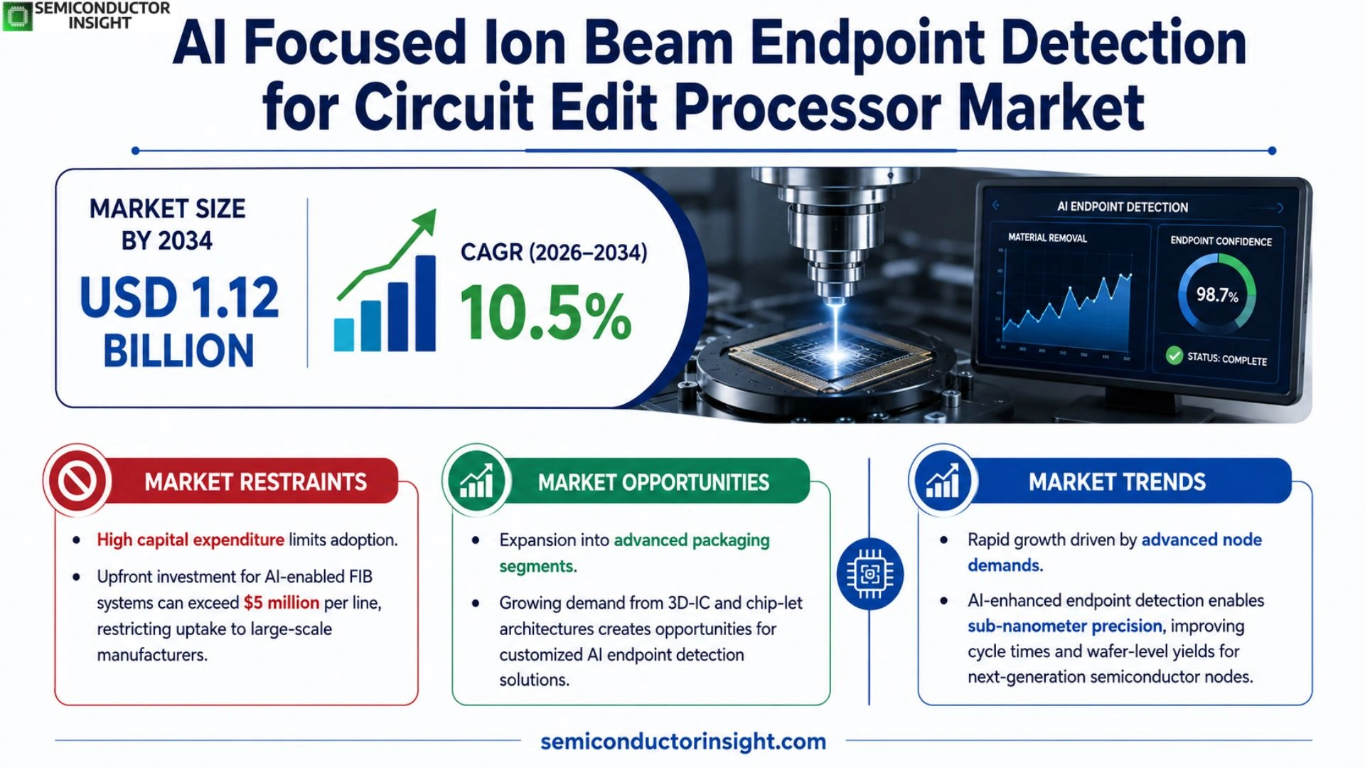
Global AI focused ion beam endpoint detection for circuit edit processor market size was valued at USD 0.42 billion in 2025. The market is projected to grow from USD 0.48 billion in 2026 to USD 1.12 billion by 2034, exhibiting a CAGR of 10.5% during the forecast period.
This technology integrates high‑precision ion beam milling with artificial‑intelligence‑driven image analysis to determine exact endpoint conditions during circuit edit operations on semiconductor wafers. By continuously monitoring material removal rates and defect formation, the system enables sub‑nanometer accuracy, reduces cycle time, and improves yield for advanced nodes such as 3 nm and below.
The market is accelerating because semiconductor manufacturers are investing heavily in next‑generation lithography and AI‑enabled process control to meet demand for high‑performance computing and mobile devices.
MARKET DRIVERS
Advanced AI Integration Enhances Process Accuracy
The infusion of deep‑learning algorithms into focused ion beam (FIB) endpoint detection has significantly reduced false‑positive rates, allowing manufacturers to achieve sub‑nanometer precision in circuit edit processes. This capability directly translates into higher yield and lower rework costs for AI Focused Ion Beam Endpoint Detection for Circuit Edit Processor Market.
Growing Demand for Miniaturized Electronics
As consumer devices shrink, the need for ultra‑fine patterning intensifies. The AI‑driven endpoint detection solution enables rapid validation of critical dimensions, supporting the accelerated timelines required by semiconductor fab lines.
➤ Industry analysts project a steady compound annual growth of 7% for AI‑enabled FIB systems through 2030, driven by the relentless push for smaller, faster chips.
Finally, the convergence of edge‑AI workloads with high‑performance computing has created a new class of processors that rely on precise circuit editing, further bolstering market momentum.
MARKET CHALLENGES
Algorithmic Complexity Increases Deployment Time
Developing robust AI models that can adapt to varying substrate materials and beam conditions remains a technical hurdle. Companies often require extensive training datasets, which prolongs time‑to‑market for new solutions.
Other Challenges
Integration with Legacy Equipment
Many fabs operate with legacy FIB hardware that lacks native support for modern AI pipelines, necessitating costly retrofits or parallel workflows.
MARKET RESTRAINTS
High Capital Expenditure Limits Adoption
The upfront investment for AI‑enabled FIB systems, including specialized GPUs and data storage infrastructure, can exceed $5 million per line. This financial barrier restricts uptake to large‑scale manufacturers, slowing broader market penetration.
MARKET OPPORTUNITIES
Expansion into Advanced Packaging Segments
Emerging 3D‑IC and chip‑let architectures require precise trenching and via formation. AI Focused Ion Beam Endpoint Detection for Circuit Edit Processor Market can capitalize on this trend by offering customized detection suites that address the unique challenges of advanced packaging.
AI Focused Ion Beam Endpoint Detection for Circuit Edit Processor Market Trends
Rapid Growth Driven by Advanced Node Demands
AI Focused Ion Beam Endpoint Detection for Circuit Edit Processor Market has demonstrated a clear upward trajectory in recent years. Valued at approximately USD 0.42 billion in 2025, the market is expected to reach USD 0.48 billion in 2026 and accelerate to USD 1.12 billion by 2034, reflecting a compound annual growth rate of roughly 10.5 percent. This expansion is anchored in the technology’s ability to deliver sub‑nanometer precision during circuit editing, a requirement that becomes increasingly critical as semiconductor manufacturers target 3 nm nodes and beyond. By continuously analyzing material removal rates and defect formation through AI‑enhanced image processing, the endpoint detection system shortens cycle times and boosts wafer‑level yields, positioning it as a strategic enabler for high‑performance computing and mobile device production.
Other Trends
Integration of AI with Ion Beam Technology
Manufacturers are embedding machine‑learning algorithms directly into ion‑beam platforms to automate endpoint determination. This integration reduces reliance on manual interpretation of microscopy data, thereby minimizing human error and increasing repeatability across production lines. Real‑time feedback loops enable dynamic adjustment of beam parameters, which translates into lower defect densities and enhanced throughput for heterogeneous integration projects. As a result, semiconductor fabs are allocating a larger share of R&D budgets to hybrid AI‑ion‑beam solutions, accelerating the diffusion of the technology throughout the supply chain.
Strategic Partnerships Accelerate Innovation
Key industry players, including Applied Materials, KLA Corporation, Hitachi High‑Technologies, and ASML, are forming strategic alliances to broaden their AI‑focused ion‑beam portfolios. Collaborative R&D initiatives focus on refining algorithmic models for endpoint prediction and expanding the compatibility of the technology with emerging lithography equipment. These partnerships not only shorten time‑to‑market for new functionalities but also create ecosystems where software and hardware vendors co‑develop standards that facilitate seamless integration into existing fab infrastructures. Consequently, the market benefits from a faster adoption cycle and a more robust pipeline of next‑generation editing tools.
COMPETITIVE LANDSCAPE
Key Industry Players
AI Focused Ion Beam Endpoint Detection – Competitive Landscape
The market is currently dominated by a handful of large semiconductor equipment manufacturers that have integrated artificial‑intelligence algorithms into their ion‑beam platforms. Applied Materials leads the segment with its AI‑enhanced circuit edit processors, leveraging extensive R&D resources to deliver sub‑nanometer endpoint accuracy for 3 nm and beyond nodes. KLA Corporation follows closely, offering high‑throughput inspection systems that combine AI‑driven image analysis with focused ion‑beam (FIB) milling, thereby shortening cycle time and improving yield. ASML has entered the space through strategic partnerships, embedding machine‑learning models into its lithography‑adjacent ion‑beam tools to provide predictive endpoint detection. These incumbents benefit from deep customer relationships, global service networks, and the ability to bundle the technology with broader process‑control suites, establishing a high barrier to entry for new entrants.
Beyond the marquee names, a range of niche and specialist firms are expanding the competitive frontier. Hitachi High‑Technologies contributes precision instrumentation and proprietary AI software that target niche high‑mix production lines. Tokyo Electron and Lam Research focus on hybrid solutions that integrate ion‑beam tools with their existing etch and deposition platforms. Smaller innovators such as Nova Measuring Instruments, Nanometrics, and Veeco Instruments provide high‑resolution metrology and feedback loops that enhance endpoint detection fidelity. Companies like Canon Tokki, Nikon, and SPTS Technologies are leveraging their expertise in equipment miniaturization to deliver cost‑effective FIB solutions for emerging heterogeneous integration applications, while Advantest and JEOL supply complementary testing and imaging hardware that completes the ecosystem.
List of Key Semiconductor Manufacturing Companies Profiled
- Applied Materials
- KLA Corporation
- ASML
- Hitachi High‑Technologies
- Tokyo Electron
- Lam Research
- Nova Measuring Instruments
- Nanometrics
- Veeco Instruments
- Canon Tokki
- Nikon
- SPTS Technologies
- Advantest
- JEOL
- Teradyne (Ultratech)
Segment Analysis:
| Segment Category | Sub-Segments | Key Insights |
| By Type |
|
Hardware‑Based AI Integration
|
| By Application |
|
Advanced Node Scaling
|
| By End User |
|
Semiconductor Fabricators
|
| By Technology Integration |
|
AI‑Enhanced Metrology Modules
|
| By Process Stage |
|
Mid‑Edit Monitoring
|
Regional Analysis: AI Focused Ion Beam Endpoint Detection for Circuit Edit Processor Market
The convergence of AI analytics with ion‑beam instrumentation drives demand, as manufacturers seek higher yields and faster time‑to‑market. Investment in AI talent and cloud‑enabled data platforms further propels adoption across leading fabs.
Stringent quality standards for advanced nodes encourage the use of AI‑enhanced detection to meet compliance thresholds, prompting fabs to upgrade inspection stacks in line with industry guidelines.
Early‑stage pilots have transitioned to production, with AI models now embedded in real‑time control loops, enabling dynamic adjustment of beam parameters based on defect predictions.
Venture capital and corporate venture arms increasingly fund startups that fuse deep‑learning frameworks with ion‑beam hardware, creating a fertile ecosystem for next‑generation solutions.
Europe
European semiconductor hubs, particularly in Germany and the Netherlands, are accelerating AI integration within ion‑beam inspection to maintain competitiveness against North American counterparts. Collaborative research programs funded by the EU foster cross‑border innovation, emphasizing sustainable manufacturing practices and reducing energy consumption through smarter defect detection. While market penetration is slower due to fragmented fab ownership, leading equipment vendors are establishing regional service centers to offer tailored AI solutions and training, strengthening Europe’s role in the global supply chain.
Asia‑Pacific
The Asia‑Pacific region, anchored by Taiwan, South Korea, and China, exhibits rapid scaling of AI Focused Ion Beam Endpoint Detection for Circuit Edit Processor technologies as demand for high‑density chips surges. Local fabs prioritize cost‑effective AI implementations, leveraging extensive data sets generated from massive production volumes. Government incentives in several countries promote R&D in AI‑enhanced lithography, driving home‑grown innovation. Nonetheless, varying regulatory environments and intellectual‑property considerations shape distinct adoption pathways across the sub‑regions.
South America
South American semiconductor activities remain nascent, but emerging investments in advanced packaging and niche fab services are creating opportunities for AI‑driven ion‑beam detection. Brazil’s technology parks host pilot projects that explore defect prediction models tailored to low‑volume, high‑value production runs. Partnerships with North American equipment suppliers provide access to cutting‑edge platforms, while local talent development programs aim to build expertise in AI for semiconductor manufacturing.
Middle East & Africa
In the Middle East and Africa, strategic initiatives focus on building foundational capabilities in semiconductor design and testing. While large‑scale fabrication is limited, regional research institutes are experimenting with AI‑assisted ion‑beam techniques to support prototype development and academic collaborations. Funding from sovereign wealth funds and technology accelerators encourages startups to explore niche applications, positioning the region as an incubation hub for future AI‑enabled inspection innovations.
Report Scope
This market research report provides a comprehensive analysis of the AI Focused Ion Beam Endpoint Detection for Circuit Edit Processor Market , covering the forecast period 2026–2034. It offers detailed insights into market dynamics, technological advancements, competitive landscape, and key trends shaping the industry.
Key focus areas of the report include:
- Market Overview: The report begins with an overview outlining its current market scenario, key growth indicators, and industry transformation drivers. It discusses macroeconomic factors, demand–supply balance, regulatory landscape, and the strategic role of semiconductors in powering advancements across industries such as automotive, telecommunications, consumer electronics, and industrial automation.
- Market Size & Forecast: Historical data and future projections for revenue, unit shipments, and market value across major regions and segments.
- Segmentation Analysis: Detailed breakdown by product type, technology, application, and end-user industry to identify high-growth segments and investment opportunities.
- Regional Insights: Insights into market performance across North America, Europe, Asia-Pacific, Latin America, and the Middle East & Africa, including country-level analysis where relevant.
- Competitive Landscape: Profiles of leading market participants, including their product offerings, R&D focus, manufacturing capacity, pricing strategies, and recent developments such as mergers, acquisitions, and partnerships.
- Technology Trends & Innovation: Assessment of emerging technologies, integration of AI/IoT, semiconductor design trends, fabrication techniques, and evolving industry standards.
- Market Drivers & Restraints: Evaluation of factors driving market growth along with challenges, supply chain constraints, regulatory issues, and market-entry barriers.
- Stakeholder Insights: Insights for component suppliers, OEMs, system integrators, investors, and policymakers regarding the evolving ecosystem and strategic opportunities.
Primary and secondary research methods are employed, including interviews with industry experts, data from verified sources, and real-time market intelligence to ensure the accuracy and reliability of the insights presented.
FREQUENTLY ASKED QUESTIONS:
What is the current market size of AI Focused Ion Beam Endpoint Detection for Circuit Edit Processor Market?
-> AI focused ion beam endpoint detection for circuit edit processor market size is projected to grow from USD 0.48 billion in 2026 to USD 1.12 billion by 2034.
Which key companies operate in AI Focused Ion Beam Endpoint Detection for Circuit Edit Processor Market?
-> Key players include Applied Materials, KLA Corporation, Hitachi High‑Technologies, and ASML, among others.
What are the key growth drivers?
-> Key growth drivers include heavy investment by semiconductor manufacturers in next‑generation lithography and AI‑enabled process control, and the rising adoption of heterogeneous integration that fuels demand for precise circuit editing tools.
Which region dominates the market?
-> Regional dominance details are not disclosed in the provided source.
What are the emerging trends?
-> Emerging trends include integration of machine‑learning algorithms into ion‑beam platforms, development of AI‑driven endpoint detection software, and alignment of ion‑beam processing with advanced nodes such as 3 nm and below.
Get Sample Report PDF for Exclusive Insights
Report Sample Includes
- Table of Contents
- List of Tables & Figures
- Charts, Research Methodology, and more...


