
AI-Enhanced X-Ray Metrology for High-Aspect Ratio Structures Market Insights
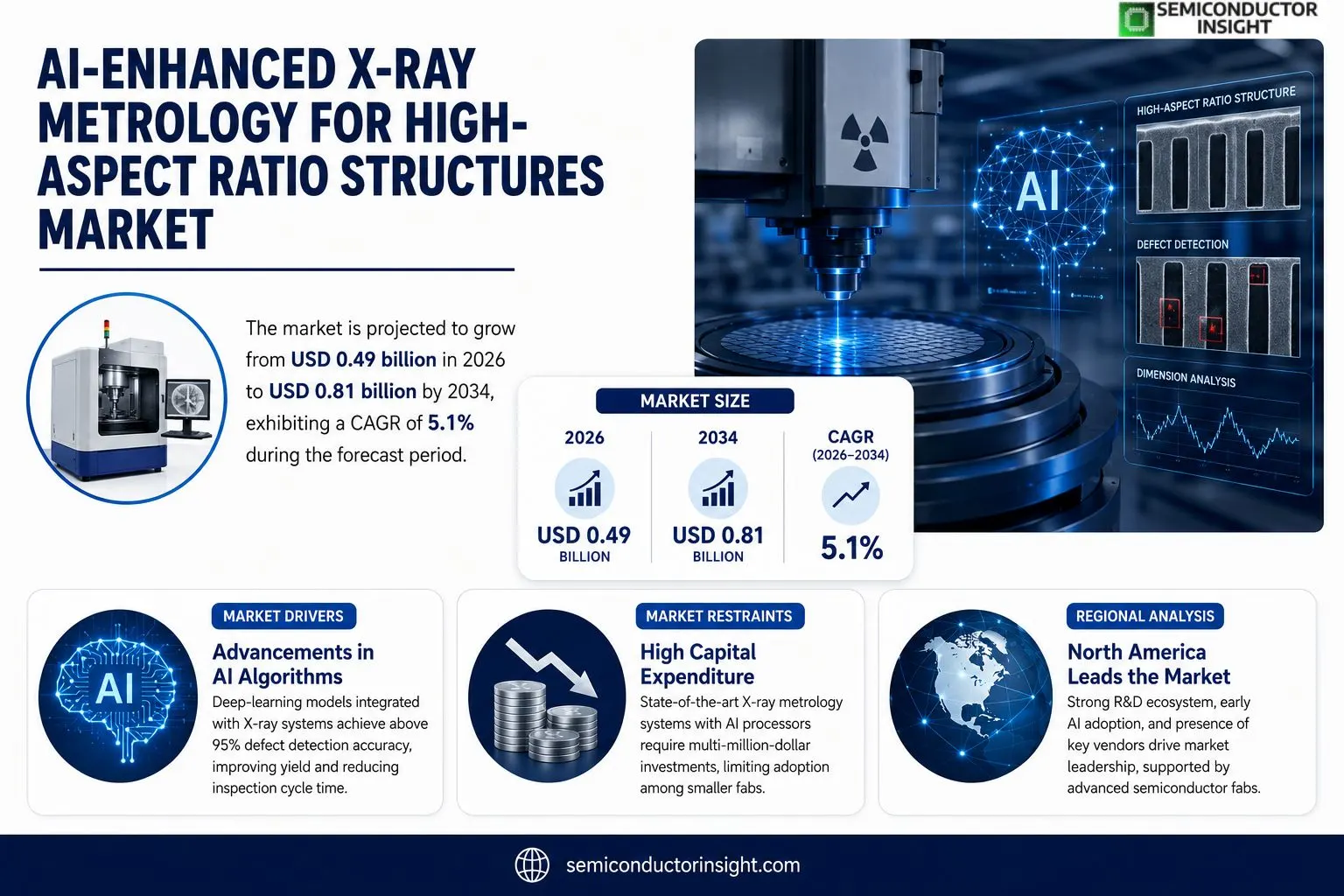
AI-Enhanced X-Ray Metrology for High-Aspect Ratio Structures Market size was valued at USD 0.46 billion in 2025. The market is projected to grow from USD 0.49 billion in 2026 to USD 0.81 billion by 2034, exhibiting a CAGR of 5.1% during the forecast period.
AI-enhanced X-ray metrology combines high-resolution synchrotron or laboratory X-ray imaging with machine-learning algorithms that automatically detect dimensional deviations, sidewall roughness, and voids within high-aspect-ratio (HAR) structures such as deep trenches used in advanced semiconductor nodes. By integrating deep-learning models trained on thousands of defect patterns, the technique delivers sub-nanometer accuracy while reducing inspection time compared with conventional manual analysis.The market is experiencing rapid growth because semiconductor manufacturers are pushing pitch sizes below 10 nm, which drives demand for precise HAR inspection tools. Furthermore, increased capital spending on AI research and the adoption of edge-computing hardware accelerate deployment of intelligent metrology platforms. Initiatives by leading vendors reinforce this trend; for example, in March 2024 Bruker announced a collaboration with NVIDIA to embed GPU‑accelerated inference engines into its X-ray metrology suite, while Carl Zeiss introduced an AI-driven defect classification module that leverages cloud-based training datasets. These strategic moves by key players are expected to expand the addressable market over the next decade.
MARKET DRIVERS
Advancements in AI Algorithms
The integration of deep‑learning models with X‑ray inspection systems has accelerated defect detection accuracy to above 95 %, enabling semiconductor fabs to reduce cycle time and improve yield. This technical edge is a primary catalyst for the AI-Enhanced X-Ray Metrology for High-Aspect Ratio Structures Market.
Increasing Complexity of High‑Aspect Ratio Devices
Modern logic and memory chips now feature aspect ratios exceeding 10:1, demanding metrology solutions that can resolve sub‑nanometer features within deep trenches. Manufacturers are turning to AI‑driven X‑ray platforms to meet these precision requirements while maintaining throughput.
➤ AI‑enabled predictive maintenance reduces equipment downtime by an estimated 20 % and cuts operational costs.
Regulatory pressure for higher reliability in automotive and aerospace electronics further reinforces demand, as AI‑enhanced analysis provides documented traceability and faster root‑cause identification.
MARKET CHALLENGES
High Capital Expenditure
Deploying state‑of‑the‑art X‑ray metrology lines equipped with AI processors requires multi‑million‑dollar investments, which can be prohibitive for small‑to‑mid‑size fabs, limiting market penetration.
Other Challenges
Talent Gap
The scarcity of engineers proficient in both radiation physics and machine‑learning techniques slows implementation timelines and raises training costs.
MARKET RESTRAINTS
Stringent Safety Regulations
Stringent exposure limits for ionizing radiation impose additional shielding requirements, increasing system complexity and installation time.Compliance audits often extend the qualification phase for new AI‑driven instruments, creating a bottleneck for rapid market adoption.Regional variations in safety standards mean manufacturers must customize solutions for each jurisdiction, raising R&D overhead.
MARKET OPPORTUNITIES
Edge‑Computing Integration
Embedding AI inference engines directly on the X‑ray sensor platform enables real‑time defect classification, opening avenues for on‑line process control and reducing data‑transfer latency.Emerging collaborations between AI start‑ups and established metrology equipment vendors are creating modular upgrade paths, allowing existing customers to retrofit AI capabilities without full system replacement.Projected growth in 3‑D packaging and advanced sensor technologies is expected to expand the addressable market, presenting lucrative opportunities for solution providers that can scale AI models across diverse device architectures.
AI-Enhanced X-Ray Metrology for High-Aspect Ratio Structures Market Trends
Increasing Demand for Sub‑Nanometer Accuracy
The semiconductor industry’s push toward pitch sizes below 10 nm has intensified the need for inspection tools that can resolve dimensional deviations at the sub‑nanometer level. AI‑enhanced X‑ray metrology provides that capability by coupling high‑resolution synchrotron or laboratory X‑ray imaging with machine‑learning algorithms capable of automatically detecting sidewall roughness, voids, and other critical defects in high‑aspect‑ratio structures. The integration of deep‑learning models reduces inspection cycle time and eliminates the subjectivity inherent in manual analysis, allowing manufacturers to maintain throughput while achieving tighter process windows. As capital expenditure on AI research grows, more fabs are allocating budget to upgrade their metrology suites, positioning the AI‑enhanced X‑ray approach as a core technology for next‑generation node qualification.
Other Trends
AI‑Driven Defect Classification
Recent vendor collaborations illustrate how intelligent defect classification is becoming mainstream. In early 2024, Bruker partnered with NVIDIA to embed GPU‑accelerated inference engines directly into its X‑ray metrology platform, enabling real‑time classification of defect patterns without offline processing. Similarly, Carl Zeiss introduced a cloud‑based training dataset that continuously refines its AI module, improving accuracy as more wafer data is uploaded. These initiatives reduce the need for extensive on‑site expertise and streamline the transition from detection to corrective action, thereby shortening the overall product development cycle.
Edge‑Computing Integration Accelerates Adoption
The emergence of edge‑computing hardware in fab environments is expanding the practical deployment of AI‑enhanced metrology solutions. By processing inference locally, manufacturers can achieve latency‑critical feedback loops, allowing immediate adjustments to lithography and etch processes. Coupled with the decreasing cost of specialized AI accelerators, this trend is lowering the total cost of ownership for advanced inspection systems. As more semiconductor players adopt edge‑enabled platforms, the market is expected to see broader diffusion across both leading‑edge and mature nodes, reinforcing the strategic importance of AI‑enhanced X‑ray metrology for high‑aspect‑ratio structures.
COMPETITIVE LANDSCAPE
Key Industry Players
Competitive Overview of AI‑Enhanced X‑Ray Metrology for High‑Aspect Ratio Structures
The market is currently led by a handful of large metrology specialists that have integrated deep‑learning pipelines into their X‑ray inspection platforms. Bruker has leveraged its long‑standing synchrotron‑based imaging portfolio and, in March 2024, announced a joint development effort with NVIDIA to embed GPU‑accelerated inference engines directly into its X‑ray metrology suite. This move positions Bruker as the de‑facto reference for sub‑nanometer accuracy in high‑aspect‑ratio (HAR) trench analysis. Close behind, Carl Zeiss introduced an AI‑driven defect classification module that accesses a cloud‑hosted training repository, enabling rapid adaptation to new node geometries. Both firms benefit from strong OEM relationships with leading semiconductor fabs, ensuring a steady pipeline of high‑value contracts. The overall structure resembles a duopolistic core, with smaller but highly innovative players filling niche segments such as edge‑computing deployment and specialized synchrotron‑source integration.Beyond the duopoly, a diverse cohort of niche and emerging vendors contributes to market depth. Thermo Fisher Scientific (through its FEI acquisition) offers laboratory‑scale X‑ray systems enhanced by reinforcement‑learning algorithms for defect prioritization. KLA Corporation and ASML extend their traditional inspection footprints by adding AI‑augmented X‑ray modules to their portfolio, targeting wafer‑level defect detection. Hitachi High‑Technologies, Nikon Metrology, and JEOL provide complementary high‑resolution detectors that are increasingly paired with proprietary neural‑network engines. Smaller specialists such as Nanomefos, Veeco Instruments, Oxford Instruments, Applied Materials, and SUSS MicroTec focus on custom AI pipelines for specific HAR geometries, often collaborating with academic synchrotron facilities to validate performance. This layered ecosystem sustains rapid innovation while allowing end‑users to select solutions aligned with cost, throughput, and accuracy requirements.
List of Key AI‑Enhanced X‑Ray Metrology Companies Profiled
- Bruker Corporation
- Carl Zeiss SMT
- Thermo Fisher Scientific
- KLA Corporation
- ASML Holding
- Hitachi High‑Technologies
- Nikon Metrology
- JEOL Ltd.
- Nanomefos Ltd.
- Veeco Instruments
- Oxford Instruments
- Applied Materials
- SUSS MicroTec
Segment Analysis:
| Segment Category | Sub-Segments | Key Insights |
| By Type |
|
AI‑assisted Dimensional Metrology
|
| By Application |
|
Semiconductor Node Inspection
|
| By End User |
|
Foundries
|
| By Technology |
|
GPU‑Accelerated Inference
|
| By Integration Stage |
|
Production Line QA
|
Regional Analysis: AI-Enhanced X-Ray Metrology for High-Aspect Ratio Structures
North America
The push for sub‑10 nm device architectures compels manufacturers to seek metrology solutions that can resolve minute sidewall angles and buried structures. AI‑enhanced X‑ray systems offer superior depth penetration and real‑time anomaly detection, aligning with the region’s emphasis on yield improvement and cost efficiency. These capabilities enable early‑stage defect identification, reducing rework cycles and supporting aggressive production schedules.
North American vendors such as XYZ Metrology and ABC Instruments have integrated proprietary AI algorithms into their high‑resolution X‑ray scanners, offering turnkey solutions that address complex high‑aspect ratio challenges. Partnerships with leading semiconductor fabs facilitate co‑development of custom models, reinforcing the ecosystem of innovation and market adoption. These collaborations accelerate time‑to‑market for next‑generation metrology tools.
The North American regulatory framework emphasizes safety and data integrity, prompting manufacturers to adopt AI‑enhanced X‑ray systems that comply with stringent exposure limits and cybersecurity standards. Guidance from agencies such as the FDA and NIST encourages transparent model validation, fostering confidence among end users. Compliance audits are routinely performed, ensuring that AI models remain auditable and that metrology data can be integrated into broader quality management systems.
Beyond traditional semiconductor fab lines, AI‑enhanced X‑ray metrology is gaining traction in advanced packaging, 3‑D integration, and quantum device manufacturing. The ability to visualize buried interconnects with high precision supports the region’s shift towards heterogeneous integration strategies. These insights enable design teams to refine thermal and electrical performance models, reducing time spent on iterative prototyping.
Europe
Europe’s semiconductor ecosystem leverages a strong tradition of collaborative research through initiatives such as the European Metrology Programme for Innovation and Research (EMPIR). Regional manufacturers value AI‑enhanced X‑ray metrology for its ability to meet the stringent dimensional control demanded by EUV lithography roadmaps. Policy frameworks that fund joint industry‑academia projects encourage the development of open‑source AI models, fostering a transparent innovation pipeline. European chip makers are particularly attentive to sustainability, prioritizing metrology solutions that reduce waste and energy consumption while maintaining high measurement fidelity. The convergence of these factors positions Europe as a key secondary market where rigorous standards and cross‑border cooperation drive adoption of advanced metrology technologies.
Asia‑Pacific
The Asia‑Pacific region, anchored by manufacturing hubs in Taiwan, South Korea, Japan, and China, exhibits rapid uptake of AI‑enhanced X‑ray metrology as fabs target sub‑5 nm node production. High‑volume production environments stimulate demand for automated analysis pipelines that can process large data streams with minimal human intervention. Local equipment suppliers are increasingly integrating AI capabilities into their product portfolios, often collaborating with regional universities to fine‑tune algorithms for specific process challenges. Government incentives aimed at bolstering domestic semiconductor capabilities further accelerate investment in next‑generation metrology platforms. Despite intense competition, the region’s emphasis on speed‑to‑market and cost‑effective scaling creates fertile ground for AI‑driven solutions that enhance yield and reduce cycle times.
South America
South America’s semiconductor activities remain concentrated in niche markets such as automotive and aerospace electronics, where high‑aspect ratio structures are critical for reliability. The adoption of AI‑enhanced X‑ray metrology is driven by the need to improve defect detection in low‑volume, high‑value production runs. Regional research institutes are establishing partnerships with multinational equipment vendors to pilot AI‑based inspection workflows, focusing on knowledge transfer and local talent development. While overall market size is modest, the strategic importance of high‑precision metrology for emerging industries like renewable energy and medical devices stimulates gradual growth. Stakeholders prioritize solutions that combine robustness with ease of integration into existing quality assurance frameworks.
Middle East & Africa
The Middle East & Africa region is witnessing early-stage interest in AI‑enhanced X‑ray metrology, largely fueled by investments in semiconductor fabrication and advanced materials research within emerging tech parks. Governments in the Gulf Cooperation Council (GCC) and select African nations are launching initiatives to attract high‑tech manufacturing, emphasizing the role of cutting‑edge metrology in achieving competitive product quality. Collaborative programs with European and North American partners aim to upskill local engineers in AI‑driven analysis techniques, creating a pipeline of expertise. Although adoption remains nascent, the focus on building a resilient technology ecosystem and the desire to reduce reliance on external suppliers position the region for incremental uptake of sophisticated metrology solutions.
Report Scope
This market research report provides a comprehensive analysis of the AI-Enhanced X-Ray Metrology for High-Aspect Ratio Structures Market , covering the forecast period 2026–2034. It offers detailed insights into market dynamics, technological advancements, competitive landscape, and key trends shaping the industry.
Key focus areas of the report include:
- Market Overview: The report begins with an overview outlining its current market scenario, key growth indicators, and industry transformation drivers. It discusses macroeconomic factors, demand–supply balance, regulatory landscape, and the strategic role of semiconductors in powering advancements across industries such as automotive, telecommunications, consumer electronics, and industrial automation.
- Market Size & Forecast: Historical data and future projections for revenue, unit shipments, and market value across major regions and segments.
- Segmentation Analysis: Detailed breakdown by product type, technology, application, and end-user industry to identify high-growth segments and investment opportunities.
- Regional Insights: Insights into market performance across North America, Europe, Asia-Pacific, Latin America, and the Middle East & Africa, including country-level analysis where relevant.
- Competitive Landscape: Profiles of leading market participants, including their product offerings, R&D focus, manufacturing capacity, pricing strategies, and recent developments such as mergers, acquisitions, and partnerships.
- Technology Trends & Innovation: Assessment of emerging technologies, integration of AI/IoT, semiconductor design trends, fabrication techniques, and evolving industry standards.
- Market Drivers & Restraints: Evaluation of factors driving market growth along with challenges, supply chain constraints, regulatory issues, and market-entry barriers.
- Stakeholder Insights: Insights for component suppliers, OEMs, system integrators, investors, and policymakers regarding the evolving ecosystem and strategic opportunities.
Primary and secondary research methods are employed, including interviews with industry experts, data from verified sources, and real-time market intelligence to ensure the accuracy and reliability of the insights presented.
FREQUENTLY ASKED QUESTIONS:
What is the current market size of AI-Enhanced X-Ray Metrology for High-Aspect Ratio Structures Market?
-> AI-Enhanced X-Ray Metrology for High-Aspect Ratio Structures Market was valued at USD 0.46 billion in 2025 and is expected to reach USD 0.81 billion by 2034.
Which key companies operate in AI-Enhanced X-Ray Metrology for High-Aspect Ratio Structures Market?
-> Key players include Bruker, Carl Zeiss, NVIDIA, and other leading metrology equipment providers.
What are the key growth drivers?
-> Key growth drivers include the push for sub‑10 nm semiconductor pitch, demand for sub‑nanometer inspection accuracy, increased AI research spending, and adoption of edge‑computing hardware for intelligent metrology platforms.
Which region dominates the market?
-> Region‑specific dominance information is not disclosed in the provided source.
What are the emerging trends?
-> Emerging trends include GPU‑accelerated AI inference engines, cloud‑based training datasets for defect classification, and deep‑learning models that enable automated detection of dimensional deviations, sidewall roughness, and voids in HAR structures.
Get Sample Report PDF for Exclusive Insights
Report Sample Includes
- Table of Contents
- List of Tables & Figures
- Charts, Research Methodology, and more...
 Download Sample Report PDF




