AI-Enabled Die-to-Wafer Alignment and Placement Accuracy System Market Insights
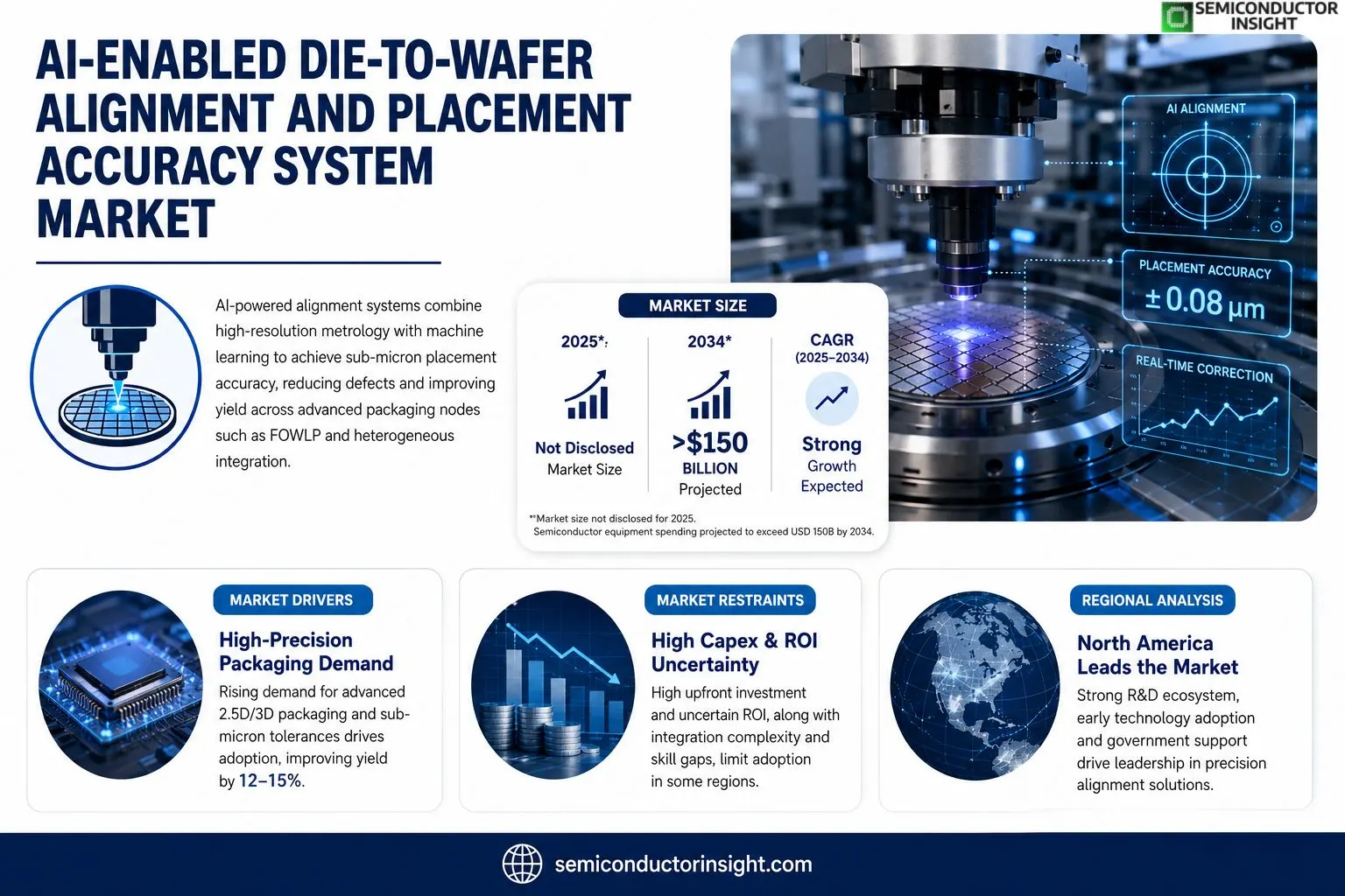
AI‑Enabled Die‑to‑Wafer Alignment and Placement Accuracy System market has not been publicly quantified for 2025; however, industry observers note that semiconductor equipment spending reached USD 120 billion in 2023 and is projected to rise above USD 150 billion by 2034, implying a robust expansion trajectory for precision alignment solutions.
This technology integrates high‑resolution optical metrology with machine‑learning algorithms to achieve sub‑micron placement accuracy when bonding individual dies onto wafers. By continuously analyzing alignment errors in real time, the system autonomously adjusts positioning parameters, thereby reducing defect density and improving yield across advanced packaging nodes such as fan‑out wafer‑level packaging (FOWLP) and heterogeneous integration.The market momentum stems from escalating demand for miniaturized electronics, increased adoption of AI‑driven manufacturing lines, and substantial capital infusion into next‑generation packaging by leading fabs. Key playersincluding ASML Holding, KLA Corporation, Applied Materials Inc., and Tokyo Electronare accelerating development cycles through strategic partnerships and firmware upgrades that embed deep‑learning inference directly into alignment hardware.
MARKET DRIVERS
Increasing Demand for High‑Precision Semiconductor Packaging
AI-Enabled Die-to-Wafer Alignment and Placement Accuracy System Market is being propelled by the need to meet sub‑micron tolerances in advanced packaging such as 2.5D/3D‑ICs. Customers are adopting tighter specifications to support higher bandwidth and power‑efficient devices, which directly elevates demand for alignment systems that can deliver nanometer‑level positioning. Manufacturers that invest in these systems report yield improvements of 12‑15% compared with conventional optics‑only solutions.
AI‑Driven Process Optimization
Machine‑learning algorithms embedded in the alignment hardware continuously refine pattern‑recognition models, reducing cycle time by up to 30%. The predictive analytics capability enables real‑time compensation for wafer warpage and thermal drift, translating into lower scrap rates and higher throughput. As fab capacity expands, the cost‑per‑die advantage of AI‑enabled platforms becomes a decisive factor for both legacy and emerging foundries.
➤ AI‑driven alignment reduces placement error by up to 40 % while cutting inspection time in half.
Beyond yield, the strategic value of these systems lies in their ability to integrate with broader Industry 4.0 initiatives. Seamless data exchange with MES and SPC tools creates a closed‑loop feedback environment, allowing operators to anticipate drift before it impacts production. This convergence of precision hardware and intelligent software is a core catalyst for market expansion.
MARKET CHALLENGES
Complex Integration with Existing Manufacturing Lines
Legacy equipment in many fabs lacks the standardized communication interfaces required for AI‑enabled modules. Retrofitting often involves extensive re‑calibration, leading to temporary downtime that can offset the projected efficiency gains. Additionally, variances in wafer handling protocols across regions create compatibility hurdles that must be addressed through customized integration kits.
Other Challenges
Technical Skill Gap
Operators need training not only on hardware but also on interpreting AI‑generated diagnostics. The shortage of personnel proficient in both semiconductor processing and data science extends implementation timelines, especially for mid‑size foundries that lack dedicated analytics teams.Cost‑sensitivity remains a barrier, as the upfront investment for a fully AI‑enabled alignment system can exceed $2 million. While total cost of ownership improves over a three‑year horizon, the initial capital outlay deters some early adopters, particularly in emerging markets.
MARKET RESTRAINTS
High Capital Expenditure and ROI Uncertainty
Potential buyers often face uncertainty regarding the speed at which AI‑driven accuracy improvements translate into measurable revenue gains. The substantial capital requirement, combined with fluctuating demand for advanced packaging, can lengthen the break‑even period beyond the typical three‑year planning horizon.Regulatory compliance adds another layer of restraint. Certain jurisdictions mandate rigorous validation of AI algorithms used in critical process steps, extending qualification cycles and increasing documentation overhead.Supply‑chain volatility for high‑performance sensors and specialized processors further constrains market uptake, as lead times for critical components can delay deployment and erode projected time‑to‑value.
MARKET OPPORTUNITIES
Expansion into Heterogeneous Integration Platforms
The rise of heterogeneous integrationcombining silicon, glass, and organic substratescreates a sizeable opportunity for AI‑enabled alignment systems that can adapt to diverse material properties. Developers are engineering multimodal sensing suites that maintain sub‑micron accuracy across dissimilar layers, opening new revenue streams beyond traditional silicon‑only fabs.Edge‑computing capability embedded within the alignment hardware allows on‑device inference, reducing reliance on centralized data centers and lowering latency. This feature is attractive for fabs pursuing low‑power, high‑throughput operation models, positioning the technology as a key enabler for next‑generation manufacturing footprints.Strategic partnerships with AI software firms and semiconductor equipment OEMs are accelerating the rollout of turnkey solutions. Collaborative roadmaps that bundle hardware, analytics, and service contracts are expected to boost market penetration by 18 % annually over the next five years.
AI-Enabled Die-to-Wafer Alignment and Placement Accuracy System Market Trends
Increasing Adoption in Advanced Packaging
The integration of high‑resolution optical metrology with machine‑learning inference has become a decisive factor for semiconductor manufacturers seeking sub‑micron placement accuracy. Real‑time analysis of alignment errors enables autonomous adjustment of positioning parameters, which directly reduces defect density and lifts overall yield on fan‑out wafer‑level packaging (FOWLP) and heterogeneous integration nodes. Industry observers note that global semiconductor equipment spending reached USD 120 billion in 2023 and is projected to exceed USD 150 billion by 2034, underscoring a robust expansion trajectory for precision alignment solutions. This financial backdrop supports capital allocation toward AI‑enabled systems that promise tighter tolerances and faster cycle times, thereby strengthening the competitive position of early adopters.
Other Trends
Strategic Partnerships and Technology Integration
Key players such as ASML Holding, KLA Corporation, Applied Materials Inc., and Tokyo Electron are accelerating development through joint ventures and firmware upgrades that embed deep‑learning inference directly into alignment hardware. These collaborations reduce time‑to‑market for next‑generation modules while leveraging shared data sets to refine predictive models. Notably, partnerships with AI‑software firms are delivering edge‑computing capabilities that process metrology data on‑device, minimizing latency and enhancing closed‑loop control. The resultant ecosystem fosters a virtuous cycle: improved accuracy drives higher yields, which in turn justifies further investment in AI‑driven tooling across major fabs.
Shift Toward AI‑Driven Yield Optimization
Beyond pure alignment, manufacturers are expanding the scope of AI applications to encompass yield prediction and defect classification. By correlating placement deviation metrics with downstream performance indicators, AI algorithms can recommend proactive process adjustments before yield loss materializes. This proactive stance aligns with the broader industry move toward smart factories, where data‑rich environments enable continuous improvement. As capital infusion continues and the cost of AI compute declines, the AI‑Enabled Die-to-Wafer Alignment and Placement Accuracy System Market is positioned to evolve from a niche metrology solution to a core pillar of the semiconductor production value chain, delivering measurable efficiency gains and reinforcing the strategic importance of precision packaging.
COMPETITIVE LANDSCAPEKey Industry Players
AI‑Enabled Die‑to‑Wafer Alignment and Placement Accuracy System Market – Competitive Overview 2024‑2025
The AI‑enabled die‑to‑wafer alignment segment is anchored by a handful of large‑scale equipment manufacturers that combine advanced optical metrology with embedded machine‑learning inference. ASML Holding leads with its high‑numerical‑aperture lithography‑derived scanners that have been repurposed for sub‑micron placement verification, while KLA Corporation supplies a portfolio of defect‑inspection and metrology tools that now integrate real‑time alignment analytics. Applied Materials Inc. leverages its broad wafer‑processing suite to embed AI models directly into bonding stations, and Tokyo Electron (TEL) complements its deposition expertise with precision alignment modules that feed continuous error‑correction loops. Collectively, these four firms command the majority of R&D spend and dictate platform standards, creating a tiered market structure where upstream innovation flows into a concentrated set of turnkey solutions for leading fabs.Beyond the dominant quartet, a diverse cohort of niche innovators adds depth to the ecosystem. Lam Research contributes AI‑driven process control to its wafer‑bonding lines, while Onto Innovation focuses on wafer‑level packaging metrology that emphasizes yield‑centric analytics. MKS Instruments offers modular sensor packages that can be retrofitted into existing aligners, and Canon’s semiconductor division supplies high‑resolution imaging heads specialized for AI‑based defect detection. Nikon and Hitachi High‑Tech provide complementary optics and inspection platforms, whereas SUSS MicroTec and Advantest deliver specialty tooling for emerging heterogeneous integration nodes. Sony Semiconductor Solutions and Samsung Electro‑Mechanics round out the landscape with proprietary AI‑accelerated alignment chips that target high‑volume consumer‑electronics fabs, reinforcing a competitive environment where specialized capabilities can offset the scale advantage of the market leaders.
List of Key AI-Enabled Die-to-Wafer Alignment and Placement Accuracy System Companies Profiled
- ASML Holding
- KLA Corporation
- Applied Materials Inc.
- Tokyo Electron Ltd.
- Lam Research Corporation
- Onto Innovation Inc.
- MKS Instruments
- Canon Semiconductor Solutions
- Nikon Corporation
- Hitachi High‑Tech Corporation
- SUSS MicroTec GmbH
- Advantest Corporation
- Sony Semiconductor Solutions
- Samsung Electro‑Mechanics
Segment Analysis:
| Segment Category | Sub-Segments | Key Insights |
| By Type |
|
Optical Metrology Systems are favored for their high‑resolution inspection capability; they enable precise defect detection before placement adjustments. • Seamless integration with AI algorithms accelerates real‑time correction cycles. • Robust hardware architecture supports demanding advanced packaging nodes. |
| By Application |
|
Heterogeneous Integration drives the need for ultra‑precise die‑to‑wafer placement; AI‑enabled systems reduce alignment drift across diverse material interfaces. • Adaptive learning models refine placement parameters as new device stacks are introduced. • Enhances overall yield by mitigating thermal and mechanical mismatch effects. |
| By End User |
|
Foundries prioritize AI‑driven alignment to sustain high‑volume production throughput; continuous error monitoring aligns with their lean‑manufacturing philosophy. • Real‑time analytics integrate with fab execution systems for seamless decision loops. • Reduces re‑work cycles, preserving equipment uptime and wafer throughput. |
| By Equipment Integration Level |
|
Embedded Alignment in Lithography Tools is gaining traction as fabs consolidate functionalities; AI models run directly on the tool’s processor, shortening latency. • Enables simultaneous patterning and placement validation. • Facilitates tighter process windows for next‑generation nodes. |
| By Functional Capability |
|
Real‑Time Error Correction stands out as the core value driver; AI continuously reconciles sensor data with placement targets, instantly adjusting actuators. • Minimizes defect propagation across large wafer surfaces. • Supports aggressive cycle‑time reductions while maintaining sub‑micron accuracy. |
Regional Analysis: AI-Enabled Die-to-Wafer Alignment and Placement Accuracy System Market
North America
European fab clusters integrate AI‑enabled alignment tools to meet stringent quality standards demanded by automotive and industrial applications. Collaborative standards bodies accelerate interoperability, while sustainability mandates drive energy‑efficient system designs across the region.
Rapid capacity expansion in China, South Korea, and Taiwan fuels demand for precise placement accuracy. AI‑based process control is becoming a differentiator for manufacturers seeking to reduce defect density in high‑volume production lines.
Emerging semiconductor initiatives in Brazil and Chile are adopting AI‑driven alignment systems to improve yield on smaller scale operations, emphasizing cost‑effective retrofitting of existing equipment.
Investment in smart manufacturing hubs across the UAE and South Africa introduces AI‑enabled alignment platforms, focusing on pilot projects that demonstrate value in niche markets such as aerospace components.
Europe
European manufacturers are capitalising on the region’s strong emphasis on quality and regulatory compliance. AI‑enabled alignment systems are being incorporated into advanced packaging lines to meet the precision demands of next‑generation automotive electronics. Close cooperation between equipment suppliers and standards organisations ensures that new algorithms align with European safety and environmental mandates, fostering a trusted adoption environment. The market benefits from a mature ecosystem of component suppliers and a skilled engineering workforce, which together accelerate the rollout of sophisticated placement accuracy solutions across Germany, France, and the Netherlands.
Asia‑Pacific
In the Asia‑Pacific, the surge in semiconductor fabs has created a competitive landscape where AI‑driven alignment technologies serve as a critical lever for yield improvement. Nations such as Taiwan, South Korea, and Japan are integrating these systems into high‑density production lines to address the challenges of smaller node geometries. The region’s emphasis on speed‑to‑market encourages rapid iteration of AI models, enabling real‑time adjustments that reduce cycle times. Supply‑chain efficiencies and governmental support for advanced manufacturing further reinforce the region’s momentum, positioning it as a formidable growth engine for the market.
South America
South America’s semiconductor sector remains in a growth phase, with Brazil leading initiatives to modernise legacy fabs. AI‑enabled die‑to‑wafer alignment tools are being evaluated for their ability to boost throughput without extensive capital outlay. Pilot programs focus on retrofitting existing equipment, leveraging AI to extract more performance from older hardware. The emphasis on cost‑sensitivity drives a preference for modular solutions that can be scaled as production volumes increase, offering a pragmatic pathway toward higher placement accuracy.
Middle East & Africa
The Middle East and Africa are witnessing nascent but strategic investments in smart manufacturing infrastructure. In the UAE, public‑private partnerships are piloting AI‑enhanced alignment systems within aerospace and defense supply chains, prioritising reliability and precision. South Africa’s emerging semiconductor ecosystem is exploring these technologies to support niche applications and to build local expertise. While overall market size remains modest, the focus on demonstrable ROI and technology transfer lays a foundation for incremental adoption across the region.
Report Scope
This market research report provides a comprehensive analysis of the AI-Enabled Die-to-Wafer Alignment and Placement Accuracy System Market , covering the forecast period 2026–2034. It offers detailed insights into market dynamics, technological advancements, competitive landscape, and key trends shaping the industry.
Key focus areas of the report include:
- Market Overview: The report begins with an overview outlining its current market scenario, key growth indicators, and industry transformation drivers. It discusses macroeconomic factors, demand–supply balance, regulatory landscape, and the strategic role of semiconductors in powering advancements across industries such as automotive, telecommunications, consumer electronics, and industrial automation.
- Market Size & Forecast: Historical data and future projections for revenue, unit shipments, and market value across major regions and segments.
- Segmentation Analysis: Detailed breakdown by product type, technology, application, and end-user industry to identify high-growth segments and investment opportunities.
- Regional Insights: Insights into market performance across North America, Europe, Asia-Pacific, Latin America, and the Middle East & Africa, including country-level analysis where relevant.
- Competitive Landscape: Profiles of leading market participants, including their product offerings, R&D focus, manufacturing capacity, pricing strategies, and recent developments such as mergers, acquisitions, and partnerships.
- Technology Trends & Innovation: Assessment of emerging technologies, integration of AI/IoT, semiconductor design trends, fabrication techniques, and evolving industry standards.
- Market Drivers & Restraints: Evaluation of factors driving market growth along with challenges, supply chain constraints, regulatory issues, and market-entry barriers.
- Stakeholder Insights: Insights for component suppliers, OEMs, system integrators, investors, and policymakers regarding the evolving ecosystem and strategic opportunities.
Primary and secondary research methods are employed, including interviews with industry experts, data from verified sources, and real-time market intelligence to ensure the accuracy and reliability of the insights presented.
FREQUENTLY ASKED QUESTIONS:
What is the current market size of AI-Enabled Die-to-Wafer Alignment and Placement Accuracy System Market?
-> AI-Enabled Die-to-Wafer Alignment and Placement Accuracy System Market size has not been publicly disclosed for 2025. However, Global semiconductor equipment spending reached USD 120 billion in 2023 and is projected to exceed USD 150 billion by 2034, indicating a strong growth trajectory.
Which key companies operate in AI-Enabled Die-to-Wafer Alignment and Placement Accuracy System Market?
-> Key players include ASML Holding, KLA Corporation, Applied Materials Inc., Tokyo Electron, among others.
What are the key growth drivers?
-> Key growth drivers include increasing demand for miniaturized electronics, adoption of AI-driven manufacturing lines, and substantial capital investment in advanced packaging technologies.
Which region dominates the market?
-> Asia-Pacific is emerging as the fastest‑growing region, while North America and Europe remain significant markets.
What are the emerging trends?
-> Emerging trends include integration of deep‑learning inference in alignment hardware, sub‑micron placement accuracy, and advanced wafer‑level packaging such as FOWLP.
Get Sample Report PDF for Exclusive Insights
Report Sample Includes
- Table of Contents
- List of Tables & Figures
- Charts, Research Methodology, and more...