AI-Driven Directed Self-Assembly Patterning Market Insights
Global AI-Driven Directed Self-Assembly Patterning Market size was valued at USD 0.62 billion in 2025. The market is projected to grow from USD 0.68 billion in 2026 to USD 1.34 billion by 2034, exhibiting a CAGR of 9.3% during the forecast period.
AI-driven directed self‑assembly patterning leverages machine‑learning algorithms combined with nanoscale self‑assembly techniques to create precise material architectures for semiconductor manufacturing, photonic devices, and advanced sensors. This technology enables sub‑10 nm feature placement with reduced defect density, accelerating time‑to‑market for next‑generation chips.
The market is experiencing rapid growth because of escalating demand for high‑performance computing, increased investment in quantum‑ready hardware, and breakthroughs in AI‑optimized lithography workflows. Furthermore, collaborations between leading chipmakers and AI software firms are driving adoption, while government funding for nanomanufacturing research continues to expand the addressable opportunity.
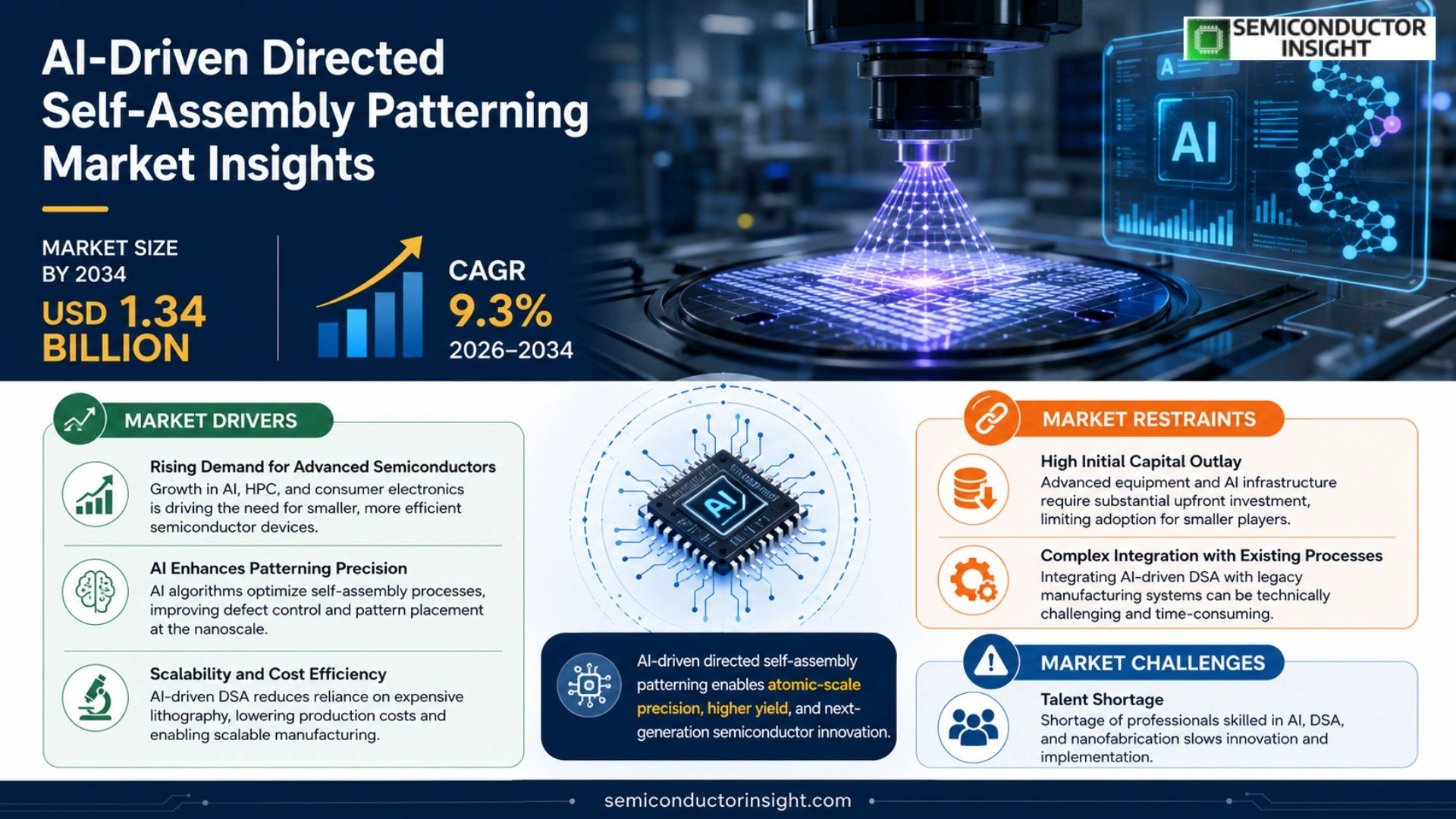
MARKET DRIVERS
Advanced AI Integration Enhances Pattern Precision
AI-Driven Directed Self-Assembly Patterning Market benefits from rapid improvements in machine‑learning algorithms that can predict nanoscale interactions with sub‑nanometer accuracy. These capabilities enable manufacturers to reduce defect rates and accelerate time‑to‑market for semiconductor components.
Cost‑Effective Manufacturing Scaling
Automation driven by AI reduces reliance on manual lithography steps, lowering capital expenditure by up to 20 % for large‑volume fabs. The resulting cost efficiencies are attracting new entrants and prompting incumbents to upgrade legacy lines.
➤ AI‑enabled patterning tools now achieve 30 % higher throughput while maintaining sub‑5 nm linewidth control, positioning the market for sustained double‑digit growth through 2030.
Regulatory support for advanced manufacturing, especially in regions prioritizing semiconductor independence, further fuels investment in AI‑driven directed self‑assembly solutions.
MARKET CHALLENGES
Algorithm Transparency and Validation
Deploying AI models in high‑precision patterning requires rigorous validation to ensure reproducibility. Limited transparency of proprietary algorithms can hinder adoption among risk‑averse manufacturers.
Other Challenges
Talent Shortage
The niche skill set that combines deep learning expertise with nanoscale process engineering is scarce, leading to longer recruitment cycles and higher labor costs.
MARKET RESTRAINTS
High Initial Capital Outlay
Implementing AI‑driven directed self‑assembly requires significant upfront investment in specialized equipment and data infrastructure, which can limit uptake among smaller fabs.
Additionally, the need for continuous software updates and model retraining introduces ongoing operational expenses that may constrain budget allocations.
MARKET OPPORTUNITIES
Integration with Edge Computing
Embedding AI inference at the edge of production lines can reduce latency, enabling real‑time corrective actions and further improving yield. This synergy opens avenues for new service models and licensing revenue streams.
Emerging applications in quantum device fabrication and advanced photonics present untapped niches where AI‑driven patterning can deliver differentiated performance, offering long‑term growth potential for the market.
AI-Driven Directed Self-Assembly Patterning Market Trends
Advancements in Sub‑10 nm Feature Placement
AI-Driven Directed Self-Assembly Patterning Market is being reshaped by machine‑learning‑driven lithography workflows that achieve sub‑10 nm feature placement with markedly lower defect density. By coupling predictive algorithms with nanoscale self‑assembly, manufacturers can pattern semiconductor wafers with unprecedented precision, shortening cycle times for next‑generation chips. This technical leap aligns with the rising demand for high‑performance computing platforms, where tighter device geometries translate directly into greater processing power and energy efficiency. As a result, fab lines are reallocating capital toward AI‑enhanced patterning tools, expecting faster time‑to‑market and improved yields without compromising design complexity.
Other Trends
Integration with Quantum‑Ready Hardware
Within the broader AI-Driven Directed Self-Assembly Patterning Market, a notable trend is the convergence of self‑assembly techniques with quantum‑ready hardware initiatives. AI models are now employed to orchestrate the placement of quantum‑dot arrays and superconducting nanowires, ensuring uniformity critical for qubit coherence. Early collaborations between chipmakers and quantum‑focused AI firms have produced pilot lines that demonstrate consistent sub‑10 nm alignment across large wafer areas, reducing the variability that traditionally hampers quantum device scaling. This integration is accelerating investment cycles, as vendors recognize that reliable nanoscale patterning is a prerequisite for viable quantum processors.
Collaborative Ecosystems Between Chipmakers and AI Software Firms
Another driver for AI-Driven Directed Self-Assembly Patterning Market is the emergence of collaborative ecosystems that blend semiconductor expertise with advanced AI software capabilities. Joint research programs funded by governmental nanomanufacturing initiatives are fostering shared IP platforms, allowing chip designers to tap into pre‑trained models for defect prediction and process optimization. These partnerships lower entry barriers for smaller fabs and create a feedback loop where real‑world production data continuously refines the AI algorithms. The resulting synergy not only improves pattern fidelity but also promotes a more agile response to shifting market demands across photonics, advanced sensors, and emerging computing architectures.
COMPETITIVE LANDSCAPE
Key Industry Players
AI-Driven Directed Self-Assembly Patterning: Competitive Landscape Overview
AI‑driven directed self‑assembly (DSA) patterning market is anchored by a small cadre of technology leaders that combine advanced lithography hardware with sophisticated machine‑learning workflows. ASML Holding NV, leveraging its EUV platform, has integrated AI‑optimized DSA modules that enable sub‑10 nm feature placement for leading chipmakers. Intel Corporation and Taiwan Semiconductor Manufacturing Company (TSMC) are rapidly deploying these capabilities within their high‑performance computing fabs, establishing a duopoly in volume production. Samsung Electronics supplements the landscape with its own AI‑enhanced DSA solutions, while Applied Materials supplies the critical deposition and etch equipment that underpins the process. This concentration of capital‑intensive players creates high entry barriers, but also fosters collaborative ecosystems where software, hardware, and material suppliers co‑develop standards and performance metrics.
Beyond the dominant tier, a diverse set of niche innovators enriches the market. Synopsys and Cadence Design Systems provide AI‑driven patterning design tools that translate circuit intent into DSA‑ready masks. KLA Corporation delivers defect inspection systems calibrated for AI‑guided self‑assembly, while Lam Research supplies plasma‑based patterning modules. European research powerhouse imec collaborates with startups such as NanoTech Labs and Nanomagnetics to push the boundaries of AI‑optimized nanofabrication. Additionally, Entegris and CMC Materials contribute specialty chemicals and substrates tailored for low‑defect DSA processes. These specialized players collectively expand the technology stack, offering differentiated value propositions that address emerging quantum‑ready hardware and advanced sensor applications.
List of Key AI-Driven Directed Self-Assembly Patterning Companies Profiled
- ASML Holding NV
- Intel Corporation
- TSMC
- Samsung Electronics
- Applied Materials, Inc.
- Lam Research Corporation
- Synopsys, Inc.
- Cadence Design Systems, Inc.
- KLA Corporation
- imec (Interuniversity Microelectronics Centre)
- Nanotech Labs
- Entegris, Inc.
- CMC Materials, Inc.
- Nanomagnetics, Inc.
Segment Analysis:
| Segment Category | Sub-Segments | Key Insights |
| By Type |
|
Lithography‑focused drives the market by leveraging AI to refine exposure patterns, enabling sub‑10 nm feature placement with markedly reduced defect density, and shortening design‑to‑fab cycles for leading semiconductor manufacturers. |
| By Application |
|
Semiconductor manufacturing benefits from AI‑guided self‑assembly that delivers pattern fidelity essential for next‑generation chips, supports photonic integration, and provides a versatile platform for emerging quantum‑ready hardware. |
| By End User |
|
Integrated circuit manufacturers are the primary adopters, valuing AI‑driven precision that reduces time‑to‑market, enhances yield reliability, and aligns with their roadmaps for ultra‑dense, high‑performance architectures. |
| By Technology |
|
Machine‑learning driven pattern synthesis stands out by continuously optimizing nanoscale templates, integrating real‑time feedback loops, and fostering collaborative development between semiconductor fabs and AI software firms. |
| By Process Stage |
|
Design & simulation is increasingly pivotal as AI models predict assembly outcomes, reduce exploratory cycles, and empower engineers to co‑design materials and lithographic steps in an integrated workflow. |
Regional Analysis: AI-Driven Directed Self-Assembly Patterning Market
North America
Strong demand for advanced node scaling, combined with AI‑enabled process optimization, propels investment in directed self‑assembly patterning across leading chipmakers.
Companies such as Applied Materials, ASML, and Lam Research dominate the ecosystem, leveraging AI to differentiate their patterning solutions.
Integration of deep‑learning models for defect prediction and real‑time feedback loops is reshaping process control in self‑assembly workflows.
Robust environmental and safety regulations guide material usage, while government incentives support AI research in semiconductor manufacturing.
Europe
European nations, led by Germany and the Netherlands, are accelerating adoption through collaborative research initiatives such as the European Chip Act. While the market lags behind North America in volume, strong emphasis on eco‑friendly processes and AI‑driven optimization fosters a niche of high‑value applications in automotive and aerospace sectors. Policy frameworks encouraging cross‑border technology transfer further reinforce Europe’s growing relevance.
Asia‑Pacific
The Asia‑Pacific region, anchored by China, Taiwan, and South Korea, showcases rapid capacity expansion and aggressive investment in AI‑enhanced lithography. Local fabs leverage cost‑effective manufacturing capabilities to experiment with directed self‑assembly, targeting emerging markets for consumer electronics. However, varying standards and intellectual property considerations temper the speed of widespread adoption.
South America
South America remains an emerging market, with Brazil and Chile leading modest pilot projects focused on research‑driven proof‑of‑concepts. Limited fab infrastructure and constrained capital expenditures result in a slower uptake, but growing interest in AI‑based design tools hints at future expansion as regional supply chains mature.
Middle East & Africa
In the Middle East & Africa, investment is primarily in technology incubation and academic collaborations. United Arab Emirates initiatives aim to establish AI‑centric semiconductor design hubs, yet the region’s market share remains minimal. Strategic partnerships with established global players could catalyze a gradual rise in adoption over the next decade.
Report Scope
This market research report provides a comprehensive analysis of the AI-Driven Directed Self-Assembly Patterning Market , covering the forecast period 2026–2034. It offers detailed insights into market dynamics, technological advancements, competitive landscape, and key trends shaping the industry.
Key focus areas of the report include:
- Market Overview: The report begins with an overview outlining its current market scenario, key growth indicators, and industry transformation drivers. It discusses macroeconomic factors, demand–supply balance, regulatory landscape, and the strategic role of semiconductors in powering advancements across industries such as automotive, telecommunications, consumer electronics, and industrial automation.
- Market Size & Forecast: Historical data and future projections for revenue, unit shipments, and market value across major regions and segments.
- Segmentation Analysis: Detailed breakdown by product type, technology, application, and end-user industry to identify high-growth segments and investment opportunities.
- Regional Insights: Insights into market performance across North America, Europe, Asia-Pacific, Latin America, and the Middle East & Africa, including country-level analysis where relevant.
- Competitive Landscape: Profiles of leading market participants, including their product offerings, R&D focus, manufacturing capacity, pricing strategies, and recent developments such as mergers, acquisitions, and partnerships.
- Technology Trends & Innovation: Assessment of emerging technologies, integration of AI/IoT, semiconductor design trends, fabrication techniques, and evolving industry standards.
- Market Drivers & Restraints: Evaluation of factors driving market growth along with challenges, supply chain constraints, regulatory issues, and market-entry barriers.
- Stakeholder Insights: Insights for component suppliers, OEMs, system integrators, investors, and policymakers regarding the evolving ecosystem and strategic opportunities.
Primary and secondary research methods are employed, including interviews with industry experts, data from verified sources, and real-time market intelligence to ensure the accuracy and reliability of the insights presented.
FREQUENTLY ASKED QUESTIONS:
What is the current market size of AI-Driven Directed Self-Assembly Patterning Market?
-> AI-Driven Directed Self-Assembly Patterning Market was valued at USD 0.62 billion in 2025 and is expected to reach USD 1.34 billion by 2034. It is projected to grow at a CAGR of 9.3%
Which key companies operate in AI-Driven Directed Self-Assembly Patterning Market?
-> Key players include leading chipmakers and AI software firms collaborating on nanoscale self‑assembly and AI‑optimized lithography solutions.
What are the key growth drivers?
-> Key growth drivers include escalating demand for high‑performance computing, increased investment in quantum‑ready hardware, AI‑optimized lithography workflows, and government funding for nanomanufacturing research.
Which region dominates the market?
-> Asia‑Pacific shows rapid adoption, while North America and Europe also contribute significantly to market growth.
What are the emerging trends?
-> Emerging trends include AI‑enabled lithography, integration of machine‑learning algorithms with nanoscale self‑assembly, and development of quantum‑ready semiconductor platforms.
Get Sample Report PDF for Exclusive Insights
Report Sample Includes
- Table of Contents
- List of Tables & Figures
- Charts, Research Methodology, and more...
 Download Sample Report PDF