
AI-Driven Copper Pillar Plating Uniformity Control Market Insights
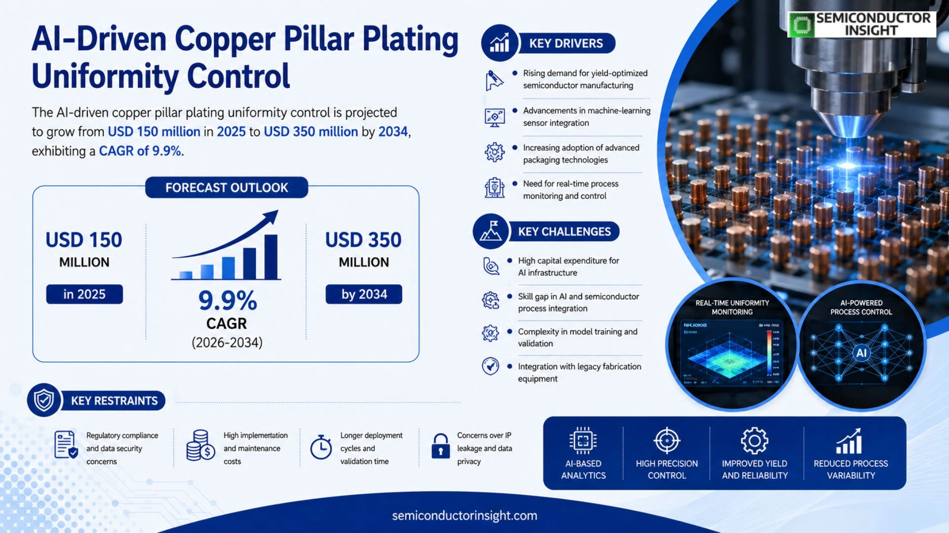
Global AI-Driven Copper Pillar Plating Uniformity Control Market size is projected to grow from USD 150 million in 2025 to USD 350 million by 2034, exhibiting a CAGR of 9.9% during the forecast period.
AI-driven copper pillar plating uniformity control refers to advanced process solutions that employ machine‑learning algorithms and real‑time sensor feedback to ensure consistent copper deposition thickness across high‑aspect‑ratio pillars used in modern semiconductor packaging. By integrating optical metrology, electrochemical modeling and predictive analytics, the technology minimizes variation, reduces defect density and enables tighter tolerances required for heterogeneous integration.
The market is experiencing rapid growth due to several factors, including heightened investment in advanced packaging, increasing demand for high‑performance computing chips and the push toward smaller node sizes where uniform copper pillars are critical. Furthermore, advancements in artificial intelligence for process optimization are lowering cycle times and improving yield, which attracts semiconductor fabs seeking cost efficiencies. Initiatives by key players such as Applied Materials, Lam Research, Tokyo Electron and KLA Corporation,who are expanding their AI‑enabled tooling portfolios,are expected to further accelerate market expansion.
MARKET DRIVERS
Rising Demand for Yield‑Optimized Semiconductor Manufacturing
AI-Driven Copper Pillar Plating Uniformity Control Market is being propelled by manufacturers’ relentless pursuit of higher yields and lower defect rates in advanced semiconductor nodes. AI‑enabled process monitoring allows real‑time adjustment of plating parameters, reducing variability by up to 30% and translating into measurable cost savings across fab lines.
Advancements in Machine‑Learning Sensor Integration
Recent breakthroughs in optical‑sensor resolution and edge‑computing platforms have lowered the latency of feedback loops, enabling precise control of copper pillar thickness across large wafers. Companies that integrate these technologies report a 15‑20% improvement in uniformity, which directly supports the market’s growth trajectory.
➤ The adoption rate of AI‑based uniformity solutions is projected to exceed 55% by 2028, driven by the need for sub‑10‑nm interconnect reliability.
Overall, the convergence of cost‑pressured production targets and maturing AI algorithms creates a compelling environment for investment, positioning AI-Driven Copper Pillar Plating Uniformity Control Market as a critical enabler of next‑generation chip performance.
MARKET CHALLENGES
High Capital Expenditure for AI Infrastructure
Deploying AI‑driven control systems requires significant upfront spending on high‑performance compute nodes, data acquisition hardware, and specialized software licenses. Smaller fabs often struggle to justify the expense against short‑term ROI, slowing broader market penetration.
Other Challenges
Skill Gap
The rapid evolution of machine‑learning models outpaces the availability of engineers proficient in both semiconductor process physics and AI development, creating a talent bottleneck that hampers seamless implementation.
MARKET RESTRAINTS
Regulatory Compliance and Data Security
Stringent industry standards for data handling and electromagnetic compatibility restrict the deployment of connected AI modules on production lines. Compliance audits add layers of procedural overhead, increasing time‑to‑market for new solutions.
Furthermore, concerns over intellectual‑property leakage when transmitting process data to cloud‑based analytics platforms deter some manufacturers from fully leveraging AI capabilities.
These regulatory and security considerations act as practical restraints, requiring vendors to invest in robust, transparent compliance frameworks before scaling offerings.
MARKET OPPORTUNITIES
Emerging Applications in Advanced Packaging
Advanced packaging formats such as fan‑out wafer‑level packaging (FOWLP) and heterogeneous integration demand ultra‑precise copper pillar placement to maintain electrical performance. AI‑driven uniformity control provides the granularity needed for these high‑density architectures, opening new revenue streams.
Additionally, the growing emphasis on sustainability in semiconductor fabs creates opportunities for AI systems that optimize material usage, reduce chemical waste, and lower energy consumption, aligning with corporate ESG goals.
Strategic partnerships between AI specialists and equipment OEMs are expected to accelerate product rollouts, positioning early adopters to capture a sizable share of the expanding market landscape.
AI-Driven Copper Pillar Plating Uniformity Control Market Trends
Increasing Adoption of AI for Process Uniformity
AI-Driven Copper Pillar Plating Uniformity Control Market is witnessing a decisive shift as semiconductor fabs prioritize process reliability and yield maximization. By embedding machine‑learning algorithms within deposition equipment, manufacturers achieve continuous monitoring of copper thickness and automatically adjust electrochemical parameters to counteract drift. This closed‑loop capability reduces the incidence of out‑of‑spec pillars and supports tighter design tolerances required for next‑generation heterogeneous integration. In addition, the ability to predict and correct deposition deviations in real time shortens overall cycle time, allowing production schedules to become more predictable while maintaining the stringent quality standards demanded by high‑performance computing applications.
Other Trends
Integration of Optical Metrology with Predictive Analytics
Optical metrology systems are now being coupled with AI‑driven predictive models to create a proactive quality assurance layer. High‑resolution inspection data feeds directly into neural networks that forecast potential non‑uniformities before they impact the wafer. This approach is especially valuable as node dimensions continue to shrink, making each copper pillar more critical to the overall electrical performance of the package. Early‑stage deployments have shown that the combined insight from optical sensing and analytics enables process engineers to tighten control limits without sacrificing throughput, thereby delivering incremental yield improvements while preserving equipment utilization.
Expansion of AI‑Enabled Tool Portfolios by Key Vendors
Major equipment suppliers,including Applied Materials, Lam Research, Tokyo Electron, and KLA Corporation,are rapidly expanding their AI‑enabled tooling offerings. Their newest platforms integrate edge‑compute processors that execute neural‑network inference on the shop floor, allowing instantaneous adjustments to plating chemistry based on live sensor feedback. This level of automation not only aligns with cost‑reduction initiatives but also simplifies the adoption curve for fabs that lack extensive data‑science resources. As these vendors continue to refine model accuracy and broaden the range of controllable parameters, the overall market momentum is reinforced, positioning AI‑driven copper pillar plating as a foundational technology for the upcoming wave of advanced semiconductor packaging.
COMPETITIVE LANDSCAPE
Key Industry Players
AI‑Driven Copper Pillar Plating Uniformity Control – Competitive Overview
Applied Materials remains the clear market leader, leveraging its deep portfolio of AI‑enabled deposition equipment to secure a dominant share of the copper‑pillar plating uniformity segment. Its integrated sensors, optical metrology and machine‑learning analytics allow fab operators to close the loop on process variation in real time, delivering yield improvements that are increasingly demanded by advanced‑node packaging lines. The market structure reflects a classic oligopoly: a handful of global equipment manufacturers own the majority of intellectual property, while smaller specialist firms focus on niche sensor or software modules that complement the larger toolsets. This concentration enables coordinated R&D investments that sustain the projected 9.9 % CAGR through 2034, yet it also creates high entry barriers for newcomers lacking comparable AI infrastructure.
Beyond the flagship players, a robust set of niche innovators is shaping the competitive dynamics. Lam Research and Tokyo Electron have accelerated their AI roadmaps, embedding predictive analytics into next‑generation electro‑plating platforms. KLA Corporation provides complementary defect‑inspection solutions that feed data back into plating control loops. ASM International, Hitachi High‑Tech and SCREEN Holdings supply precision‑tuned hardware and surface‑treatment chemistries that differentiate regional fab offerings. Companies such as Besi, Nanomaterial Technologies, Entegris and Advantest contribute specialized sensor arrays, ultra‑pure chemicals, and high‑speed data acquisition modules that are increasingly integrated as plug‑in components for the larger OEM ecosystems. Collectively, these players expand the value chain, foster technology diversification, and intensify competitive pressure on pricing and innovation cycles.
List of Key AI‑Driven Copper Pillar Plating Uniformity Control Companies Profiled
- Applied Materials
- Lam Research
- Tokyo Electron
- KLA Corporation
- ASM International
- Hitachi High‑Tech
- SCREEN Holdings
- Besi
- Nanomaterial Technologies
- Entegris
- Advantest
- Nanofilm Technologies
- MeasureX
- Camtek
- Teradyne
Segment Analysis:
| Segment Category | Sub-Segments | Key Insights |
| By Type |
|
Machine‑Learning Algorithmic Control
|
| By Application |
|
High‑Aspect‑Ratio Pillar Deposition
|
| By End User |
|
Semiconductor Fabrication Fabs
|
| By Technology |
|
Predictive Analytics Platforms
|
| By Process Stage |
|
In‑Process Monitoring
|
Regional Analysis: AI-Driven Copper Pillar Plating Uniformity Control Market
AI platforms are entrenched in the fab’s control hierarchy, enabling predictive adjustments during deposition. Edge computing reduces latency, while cloud‑based model training incorporates data from multiple fabs, fostering cross‑plant learning and accelerating innovation cycles.
Environmental compliance standards encourage precise metal usage, prompting fabs to adopt AI‑driven uniformity controls. Agencies endorse data‑driven process documentation, reinforcing the business case for algorithmic monitoring and reporting.
Major equipment vendors partner with AI specialists to embed analytics in plating tools. Start‑ups focusing on defect detection secure strategic alliances, expanding the solution stack beyond mere uniformity measurement to predictive maintenance.
The demand for high‑purity copper and calibrated deposition chemicals is steadied by AI‑guided inventory forecasting, reducing lead times and mitigating material shortages across the value chain.
Europe
European semiconductor hubs are transitioning from pilot projects to full‑scale deployment of AI‑driven uniformity controls. The region benefits from strong public‑private research initiatives that blend academic expertise with industry needs, fostering a collaborative ecosystem. While adoption rates lag behind North America, stringent EU environmental directives create a compelling incentive for precise copper usage, driving incremental uptake across flagship fabs in Germany and the Netherlands.
Asia‑Pacific
Asia‑Pacific presents a rapidly expanding landscape, with China, Taiwan, and South Korea accelerating investments in AI‑enhanced plating processes to support burgeoning 3‑nm and beyond production. The market is characterized by a high degree of cost sensitivity, prompting manufacturers to focus on AI solutions that deliver clear yield improvements. Local vendors increasingly offer bundled hardware‑software packages tailored to regional fab architectures, fostering a competitive environment that spurs innovation.
South America
South American semiconductor activities remain modest, yet emerging research centers are experimenting with AI‑based process control to attract downstream manufacturing. Brazil’s technology parks are piloting collaborative projects that integrate AI analytics with existing plating equipment, aiming to reduce material waste and improve product consistency. These initiatives lay groundwork for future market entry as the region seeks to diversify its high‑tech portfolio.
Middle East & Africa
The Middle East & Africa region is in the early awareness stage, with a handful of strategic partnerships forming between multinational equipment suppliers and local research institutes. Initiatives focus on knowledge transfer and capacity building, emphasizing the long‑term benefits of AI‑driven copper pillar plating uniformity. While commercial deployment is limited, the region’s investment in smart manufacturing infrastructure positions it to adopt the technology as its semiconductor ecosystem matures.
Report Scope
This market research report provides a comprehensive analysis of the AI-Driven Copper Pillar Plating Uniformity Control Market , covering the forecast period 2026–2034. It offers detailed insights into market dynamics, technological advancements, competitive landscape, and key trends shaping the industry.
Key focus areas of the report include:
- Market Overview: The report begins with an overview outlining its current market scenario, key growth indicators, and industry transformation drivers. It discusses macroeconomic factors, demand–supply balance, regulatory landscape, and the strategic role of semiconductors in powering advancements across industries such as automotive, telecommunications, consumer electronics, and industrial automation.
- Market Size & Forecast: Historical data and future projections for revenue, unit shipments, and market value across major regions and segments.
- Segmentation Analysis: Detailed breakdown by product type, technology, application, and end-user industry to identify high-growth segments and investment opportunities.
- Regional Insights: Insights into market performance across North America, Europe, Asia-Pacific, Latin America, and the Middle East & Africa, including country-level analysis where relevant.
- Competitive Landscape: Profiles of leading market participants, including their product offerings, R&D focus, manufacturing capacity, pricing strategies, and recent developments such as mergers, acquisitions, and partnerships.
- Technology Trends & Innovation: Assessment of emerging technologies, integration of AI/IoT, semiconductor design trends, fabrication techniques, and evolving industry standards.
- Market Drivers & Restraints: Evaluation of factors driving market growth along with challenges, supply chain constraints, regulatory issues, and market-entry barriers.
- Stakeholder Insights: Insights for component suppliers, OEMs, system integrators, investors, and policymakers regarding the evolving ecosystem and strategic opportunities.
Primary and secondary research methods are employed, including interviews with industry experts, data from verified sources, and real-time market intelligence to ensure the accuracy and reliability of the insights presented.
FREQUENTLY ASKED QUESTIONS:
What is the current market size of AI-Driven Copper Pillar Plating Uniformity Control Market?
-> AI-Driven Copper Pillar Plating Uniformity Control Market was valued at USD 150 million in 2025 and is expected to reach USD 350 million by 2034.
Which key companies operate in AI-Driven Copper Pillar Plating Uniformity Control Market?
-> Key players include Applied Materials, Lam Research, Tokyo Electron, and KLA Corporation, among others.
What are the key growth drivers?
-> Key growth drivers include increased investment in advanced semiconductor packaging, rising demand for high‑performance computing chips, and the push toward smaller process nodes requiring uniform copper pillars.
Which region dominates the market?
-> The reference does not specify a single dominant region; market expansion is observed globally with strong activity in major semiconductor hubs.
What are the emerging trends?
-> Emerging trends include AI‑enabled process optimization, real‑time sensor feedback for thickness control, and integration of predictive analytics in copper pillar deposition.

Get Sample Report PDF for Exclusive Insights
Report Sample Includes
- Table of Contents
- List of Tables & Figures
- Charts, Research Methodology, and more...
 Download Sample Report PDF





