
AI-Driven Carrier Lifetime Measurement and Mapping Tool Market Insights
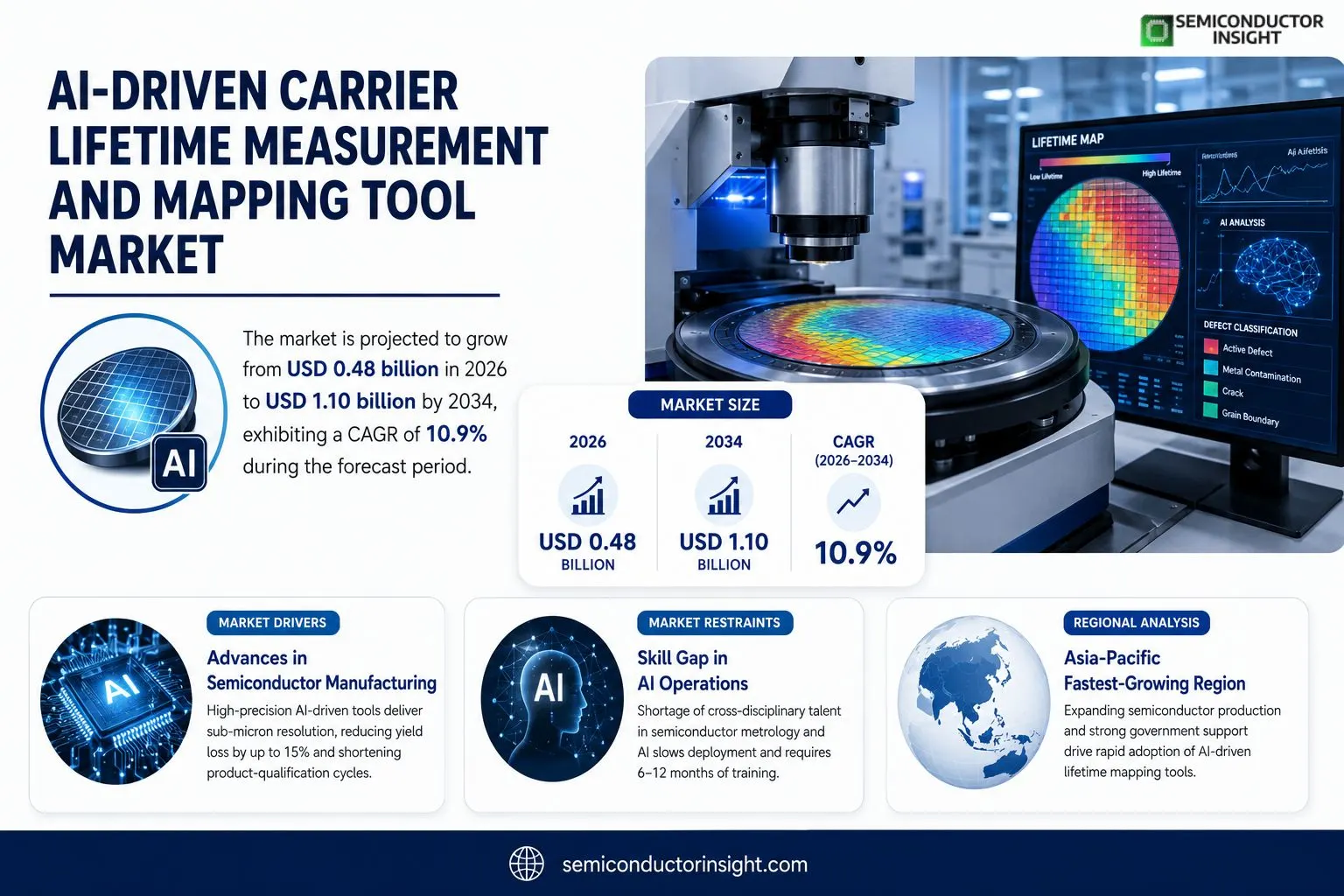
AI-Driven Carrier Lifetime Measurement and Mapping Tool market size was valued at USD 0.45 billion in 2025. The market is projected to grow from USD 0.48 billion in 2026 to USD 1.10 billion by 2034, exhibiting a CAGR of 10.9% during the forecast period.
AI-driven carrier lifetime measurement and mapping tools are advanced instrumentation that combine photoluminescence imaging, microwave‑detected photoconductance, and machine‑learning analytics to quantify minority‑carrier recombination lifetimes across semiconductor wafers. These systems enable high‑resolution spatial mapping, rapid data processing, and predictive defect classification, supporting process optimization in photovoltaic manufacturing and research.The market is experiencing rapid growth because semiconductor manufacturers are scaling up production of high‑efficiency solar cells while research institutions demand precise lifetime diagnostics for emerging materials such as perovskites. Furthermore, rising capital expenditure on smart‑factory automation and the integration of AI algorithms for defect prediction are accelerating adoption; key players including Hamamatsu Photonics, MKS Instruments, and LightTech Instruments have announced new product launches and strategic partnerships in recent years.
MARKET DRIVERS
Advances in Semiconductor Manufacturing
The rapid scaling of silicon photovoltaics and power‑electronics devices demands higher precision in defect detection, and AI‑driven carrier lifetime measurement and mapping tools provide sub‑micron resolution that traditional metrology cannot achieve. Manufacturers are adopting these solutions to reduce yield loss by up to 15 % while shortening product‑qualification cycles.
Integration of Artificial Intelligence
Machine‑learning algorithms now enable real‑time analysis of lifetime maps, automatically flagging anomalous regions and recommending process adjustments. This predictive capability accelerates root‑cause analysis and supports continuous‑improvement initiatives across fabs.
➤ “AI‑powered lifetime mapping has cut defect‑identification time from days to hours, directly boosting throughput.”
Governments worldwide are increasing funding for renewable‑energy research, which translates into higher capital expenditure for PV production lines. The AI‑Driven Carrier Lifetime Measurement and Mapping Tool Market benefits from this fiscal momentum, as end‑users prioritize tools that can validate material quality under tighter efficiency targets.
MARKET CHALLENGES
High Initial Capital Outlay
Although the long‑term ROI is attractive, the upfront cost of a fully integrated AI‑driven system often exceeds $500 k, creating budgetary barriers for small‑ and medium‑sized enterprises seeking to modernize their test lines.
Other Challenges
Data Security Concerns
The reliance on cloud‑based analytics raises questions about proprietary process data protection, prompting some manufacturers to delay adoption until robust encryption standards are demonstrated.
MARKET RESTRAINTS
Skill Gap in AI Operations
Effective use of these tools requires personnel skilled in both semiconductor metrology and machine‑learning techniques. The shortage of such cross‑disciplinary talent slows deployment, as firms must invest in training programs that can take 6‑12 months to mature.
MARKET OPPORTUNITIES
Emerging Applications in Wide‑Bandgap Materials
Silicon‑carbide (SiC) and gallium‑nitride (GaN) devices are gaining traction in electric‑vehicle powertrains. AI‑driven lifetime mapping can uniquely characterize defect dynamics in these wide‑bandgap substrates, opening a lucrative niche for tool vendors who tailor algorithms to the distinct carrier‑recombination mechanisms of SiC and GaN.
AI-Driven Carrier Lifetime Measurement and Mapping Tool Market Trends
Integration of AI for High‑Resolution Lifetime Mapping
Artificial‑intelligence algorithms are increasingly embedded within carrier‑lifetime measurement platforms to convert raw photoluminescence and microwave‑detected photoconductance data into actionable defect maps. The synergy of machine‑learning analytics with high‑resolution imaging enables real‑time identification of minority‑carrier recombination sites across entire semiconductor wafers. This capability shortens feedback loops in process development, allowing manufacturers to adjust deposition or annealing parameters within a single production shift. Furthermore, standardized data formats facilitate integration with manufacturing execution systems, supporting cross‑factory analytics and benchmarking. As a result, yield improvements and cost reductions are becoming measurable outcomes for early adopters.
Other Trends
Adoption in Photovoltaic Manufacturing
Solar‑cell producers are deploying AI‑driven lifetime tools to monitor the quality of emerging high‑efficiency architectures, including heterojunction and perovskite layers. The instruments provide spatially resolved lifetime values that correlate directly with cell performance, supporting defect classification that was previously reliant on time‑consuming manual microscopy. By integrating these measurements into automated test lines, factories achieve a higher degree of process uniformity, which translates into consistent power output across large‑area modules. The rapid data processing also enables inline decision‑making, reducing the time required to move from wafer inspection to equipment adjustment.
Strategic Partnerships and Product Innovation
Key suppliers such as Hamamatsu Photonics, MKS Instruments, and LightTech Instruments have announced collaborative projects with semiconductor research institutes to co‑develop next‑generation mapping solutions. These partnerships focus on extending wavelength coverage, improving signal‑to‑noise ratios, and embedding predictive maintenance modules that alert operators to equipment drift before it impacts data quality. The combined effect of joint R&D and expanded product portfolios is accelerating market penetration beyond the traditional research segment into full‑scale manufacturing environments. Customers report a reduction of die‑to‑die variability by up to 15 %, which improves overall module efficiency and strengthens the business case for capital investment.
COMPETITIVE LANDSCAPE
Key Industry Players
AI‑Driven Carrier Lifetime Measurement and Mapping Tool Market Competitive Overview
The market is currently led by a handful of well‑capitalized instrument manufacturers that have integrated AI modules into legacy photoluminescence and microwave‑detected photoconductance platforms. Hamamatsu Photonics holds a clear leadership position thanks to its high‑sensitivity PL imaging systems, robust AI‑based defect classification software, and strategic alliances with major solar‑cell fabs in Asia and Europe. Its recent launch of the “QuantumScope AI” suite has expanded the addressable market, reinforcing a concentration of market share among three to five large players that command the majority of OEM contracts and large‑scale research grants.Beyond the dominant incumbents, a vibrant set of niche innovators is shaping specialized segments of the ecosystem. MKS Instruments leverages its expertise in microwave‑based carrier‑lifetime diagnostics, while LightTech Instruments focuses on ultra‑high‑resolution mapping for perovskite research. NovaSci Instruments, CSEM, and Advantest contribute differentiated sensor architectures and AI‑driven analytics for thin‑film and tandem‑cell applications. Smaller firms such as Anritsu, Thorlabs, Nikon, Olympus, Oxford Instruments, Solmetrics, STI Instruments, Viavi Solutions, and Spectra‑Physics round out the competitive landscape, offering complementary hardware, custom software stacks, or region‑specific services that increase choice for end users and foster continuous innovation.
List of Key AI‑Driven Carrier Lifetime Measurement and Mapping Tool Companies Profiled
- Hamamatsu Photonics
- MKS Instruments
- LightTech Instruments
- CSEM
- NovaSci Instruments
- Advantest
- Anritsu
- Thorlabs
- Nikon
- Olympus
- Oxford Instruments
- Solmetrics
- STI Instruments
- Viavi Solutions
- Spectra‑Physics
Segment Analysis:
| Segment Category | Sub-Segments | Key Insights |
| By Type |
|
Photoluminescence Lifetime Tools
|
| By Application |
|
Photovoltaic Cell Manufacturing
|
| By End User |
|
Solar Panel Manufacturers
|
| By Technology |
|
Integrated AI‑Embedded Instruments
|
| By Market Driver |
|
AI‑Enabled Defect Prediction
|
Regional Analysis: AI-Driven Carrier Lifetime Measurement and Mapping Tool Market
North America
Leading equipment manufacturers are forging strategic partnerships with AI software providers to embed predictive analytics directly into carrier lifetime measurement instruments. These collaborations accelerate product rollout cycles and create joint go‑to‑market strategies that address specific wafer‑level reliability challenges, reinforcing North America’s market momentum. Such alliances also facilitate co‑development of customized data pipelines, enhancing real‑time decision support for fab engineers.
Significant capital is being allocated to R&D initiatives focused on deep‑learning algorithms that interpret lifetime maps with higher spatial resolution. Universities and corporate labs partner to explore novel photon‑counting detectors, aiming to boost measurement sensitivity while reducing acquisition time. These investments cement the region’s technological edge.
Regulatory bodies in the United States and Canada encourage adoption of AI‑driven metrology through incentives tied to energy efficiency and yield improvement. Standards organizations are updating test protocols to incorporate AI‑derived lifetime metrics, ensuring consistency across fabs and facilitating cross‑border collaborations.
Fab operators across the region are increasingly integrating AI‑driven lifetime measurement tools into their production lines to enable predictive maintenance and defect isolation. Early adopters report faster root‑cause analysis, leading to decreased downtime and higher overall equipment effectiveness.
Europe
Europe remains a dynamic hub for AI-Driven Carrier Lifetime Measurement and Mapping Tool Market, with Germany, France, and the Netherlands spearheading innovation through strong industrial consortia. European manufacturers benefit from the EU’s Horizon Europe funding, which underwrites collaborative projects that blend AI techniques with advanced photonics. The emphasis on sustainability drives the deployment of lifetime mapping to reduce material waste and improve energy efficiency in semiconductor fabs. While regulatory frameworks are rigorous, they provide a clear pathway for validation of AI‑enhanced measurement solutions, fostering confidence among end‑users.
Asia‑Pacific
The Asia‑Pacific region, led by China, Taiwan, South Korea, and Japan, demonstrates rapid growth in AI-Driven Carrier Lifetime Measurement and Mapping Tool Market, propelled by expanding fabrication capacities and aggressive technology roadmaps. Strong governmental support for semiconductor self‑sufficiency fuels investment in AI‑based metrology platforms that can handle high‑volume production. Local equipment vendors are integrating AI modules into legacy measurement tools, offering cost‑effective upgrades for mid‑size fabs. Competitive pressure encourages continuous improvement in data analytics, positioning the region as a formidable contender in the landscape.
South America
In South America, Brazil and Mexico are emerging as key contributors to AI-Driven Carrier Lifetime Measurement and Mapping Tool Market, driven by increasing domestic semiconductor initiatives and foreign investment. Although the market size remains modest, the adoption of AI‑enhanced lifetime tools is accelerating as manufacturers seek to improve yield and reduce reliance on imported metrology equipment. Collaborative programs with North American partners provide technology transfer and training, enabling local fabs to implement advanced analytics within their process flows.
Middle East & Africa
The Middle East & Africa region shows nascent yet promising activity within AI-Driven Carrier Lifetime Measurement and Mapping Tool Market. United Arab Emirates and Saudi Arabia are investing in research parks and partnering with technology firms to establish localized capabilities. While the semiconductor manufacturing base is limited, the focus on renewable energy and advanced materials creates opportunities for applying carrier lifetime mapping in photovoltaic and power device testing. Early pilot projects aim to build expertise and lay the groundwork for future expansion as regional demand for high‑performance electronics grows.
Report Scope
This market research report provides a comprehensive analysis of the AI-Driven Carrier Lifetime Measurement and Mapping Tool Market , covering the forecast period 2026–2034. It offers detailed insights into market dynamics, technological advancements, competitive landscape, and key trends shaping the industry.
Key focus areas of the report include:
- Market Overview: The report begins with an overview outlining its current market scenario, key growth indicators, and industry transformation drivers. It discusses macroeconomic factors, demand–supply balance, regulatory landscape, and the strategic role of semiconductors in powering advancements across industries such as automotive, telecommunications, consumer electronics, and industrial automation.
- Market Size & Forecast: Historical data and future projections for revenue, unit shipments, and market value across major regions and segments.
- Segmentation Analysis: Detailed breakdown by product type, technology, application, and end-user industry to identify high-growth segments and investment opportunities.
- Regional Insights: Insights into market performance across North America, Europe, Asia-Pacific, Latin America, and the Middle East & Africa, including country-level analysis where relevant.
- Competitive Landscape: Profiles of leading market participants, including their product offerings, R&D focus, manufacturing capacity, pricing strategies, and recent developments such as mergers, acquisitions, and partnerships.
- Technology Trends & Innovation: Assessment of emerging technologies, integration of AI/IoT, semiconductor design trends, fabrication techniques, and evolving industry standards.
- Market Drivers & Restraints: Evaluation of factors driving market growth along with challenges, supply chain constraints, regulatory issues, and market-entry barriers.
- Stakeholder Insights: Insights for component suppliers, OEMs, system integrators, investors, and policymakers regarding the evolving ecosystem and strategic opportunities.
Primary and secondary research methods are employed, including interviews with industry experts, data from verified sources, and real-time market intelligence to ensure the accuracy and reliability of the insights presented.
FREQUENTLY ASKED QUESTIONS:
What is the current market size of AI-Driven Carrier Lifetime Measurement and Mapping Tool Market?
-> AI-Driven Carrier Lifetime Measurement and Mapping Tool Market was valued at USD 0.45 billion in 2025 and is expected to reach USD 1.10 billion by 2034, representing a CAGR of 10.9% during the forecast period.
Which key companies operate in AI-Driven Carrier Lifetime Measurement and Mapping Tool Market?
-> Key players include Hamamatsu Photonics, MKS Instruments, LightTech Instruments, among others.
What are the key growth drivers?
-> Key growth drivers include scaling of high‑efficiency solar cell production, demand for precise lifetime diagnostics in emerging materials such as perovskites, and increased capital expenditure on smart‑factory automation with AI‑driven defect prediction.
Which region dominates the market?
-> Asia-Pacific is the fastest‑growing region, while Europe remains a dominant market.
What are the emerging trends?
-> Emerging trends include integration of machine‑learning analytics for predictive defect classification, hybrid photoluminescence‑microwave measurement platforms, and AI‑enabled real‑time wafer mapping solutions.

Get Sample Report PDF for Exclusive Insights
Report Sample Includes
- Table of Contents
- List of Tables & Figures
- Charts, Research Methodology, and more...
 Download Sample Report PDF




