
AI Defect Inspection System for Wafers Market Insights
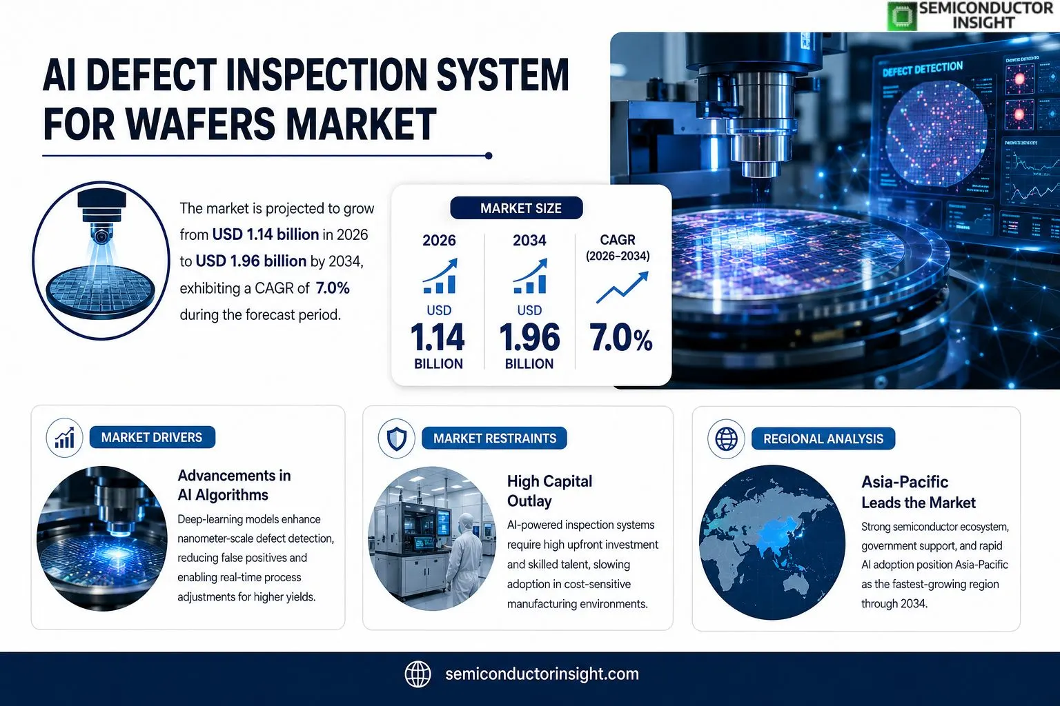
AI defect inspection system for wafers market size was valued at USD 1.08 billion in 2025. The market is projected to grow from USD 1.14 billion in 2026 to USD 1.96 billion by 2034, exhibiting a CAGR of 7.0% during the forecast period.
AI defect inspection systems employ machine‑learning algorithms and high‑resolution imaging to identify pattern anomalies on semiconductor wafers faster than conventional rule‑based tools. By correlating optical or electron‑beam data with historical failure modes, these platforms reduce false‑positive rates and enable real‑time process adjustments across front‑end manufacturing lines.The market is gaining momentum because semiconductor fabs are under pressure to improve yield while scaling node sizes below 10 nm. Investments in advanced lithography and the shift toward heterogeneous integration increase the volume of critical layers that require precise defect detection. Consequently, leading vendors such as KLA Corp., Applied Materials, Hitachi High‑Tech and Nikon Metrology are expanding their AI‑enabled portfolios and forming partnerships with cloud‑AI providers to accelerate deployment.
MARKET DRIVERS
Advancements in AI Algorithms
The integration of deep‑learning models into wafer inspection equipment has sharpened defect detection at the nanometer scale. These algorithms learn from thousands of labeled patterns, allowing the system to differentiate true anomalies from process noise with unprecedented precision.
Escalating Yield Pressures
Foundries are operating at sub‑20 nm nodes where a single undetected flaw can jeopardize an entire batch. The financial incentive to shave even a fraction of a percent off defect rates translates into sizable cost avoidance, prompting manufacturers to adopt AI‑enabled inspection tools.
➤ AI‑based inspection can cut false‑reject rates by roughly a third compared with conventional rule‑based systems.
Beyond defect reduction, the technology streamlines data collection, feeding real‑time analytics into process control loops. This closed‑feedback capability shortens cycle times and positions AI Defect Inspection System for Wafers Market as a strategic lever for productivity gains.
MARKET CHALLENGES
High Capital Outlay
Deploying an AI‑powered inspection line often requires retrofitting existing fab infrastructure, a move that can strain capital budgets already allocated for lithography upgrades. Decision‑makers must weigh the upfront expense against downstream yield improvements, a calculation that slows adoption in cost‑sensitive plants.
Other Challenges
Talent Gap
Qualified data scientists and optical engineers who can calibrate and maintain sophisticated AI models are scarce. The shortage forces many manufacturers to rely on external consultants, adding operational complexity and increasing long‑term support costs.
MARKET RESTRAINTS
Regulatory Scrutiny
Quality standards such as ISO 26262 for automotive semiconductors impose strict validation protocols on inspection software. Any AI model must undergo exhaustive verification, a process that can delay product launches and elevate compliance costs.Additionally, data privacy regulations in key regions limit the cross‑border transfer of wafer imagery, complicating collaborative model training initiatives that rely on shared datasets.These regulatory and legal constraints temper the speed at which new AI inspection solutions can be rolled out across fabs.
MARKET OPPORTUNITIES
Edge‑Computing Integration
Embedding inference engines directly onto inspection hardware reduces latency, enabling real‑time defect correction without interrupting wafer flow. Early adopters that master edge deployment can claim superior throughput and lower operational expense.The growing adoption of 300 mm wafer platforms opens a niche for AI modules that can scale with larger substrates while maintaining pixel‑level accuracy. Vendors that tailor algorithms for this format are positioned to capture a share of the expanding high‑volume market.
Finally, partnerships with semiconductor equipment OEMs create bundled offerings where AI inspection is sold as a standard feature rather than an optional add‑on, accelerating market penetration across mid‑range fabs.
AI Defect Inspection System for Wafers Market Trends
Yield Enhancement Through AI‑Enabled Defect Detection
Semiconductor manufacturers are confronting tighter tolerances as node dimensions dip below 10 nm. Traditional rule‑based inspection tools struggle to differentiate between benign pattern variations and true process failures, leading to unnecessary rework and lost throughput. AI Defect Inspection System for Wafers Market addresses this friction by layering machine‑learning classifiers on top of high‑resolution imaging, allowing the system to learn from historic defect libraries and to prioritize anomalies that are statistically linked to yield loss. This capability improves the signal‑to‑noise ratio of defect reports, shortens the feedback loop to equipment engineers, and ultimately supports higher wafer throughput without sacrificing quality.
Other Trends
AI Integration with Cloud‑Based Analytics
Vendors such as KLA Corp. and Applied Materials have begun bundling their inspection platforms with public‑cloud AI services, creating a hybrid deployment model that leverages on‑site data acquisition and remote compute power. This approach reduces the upfront investment in on‑premise GPU clusters while granting fabs access to continuously updated model weights and shared defect knowledge bases. Partnerships with cloud providers also enable scalable storage of terabytes of wafer imagery, facilitating cross‑fab benchmarking and faster identification of emerging failure modes across the supply chain.
Strategic Shift Toward Heterogeneous Integration Inspection
The move toward heterogeneous integrationstacking logic, memory, and photonic layers on a single dieexpands the number of interfaces that must be inspected for micro‑defects. Within this evolving landscape, AI Defect Inspection System for Wafers Market is seeing a rise in solutions that combine optical and electron‑beam data streams, delivering a more holistic view of layer‑to‑layer interactions. Customers are demanding tools that can flag defects in real time so that process adjustments can be enacted before the wafer proceeds to the next fabrication stage. Companies that can embed AI inference directly into the metrology hardware are positioned to capture premium contracts from fabs eager to mitigate costly yield penalties associated with increasingly complex device architectures.
COMPETITIVE LANDSCAPE
Key Industry Players
AI‑driven wafer defect inspection is reshaping yield management across advanced fabs
The market’s architecture is dominated by a handful of incumbents that have leveraged deep‑learning pipelines to upgrade legacy optical‑review tools. KLA Corp. commands a sizable share by integrating high‑throughput cameras with proprietary neural‑net classifiers, allowing fabs to flag sub‑10 nm anomalies in real time. Applied Materials complements this position through its modular inspection suites that fuse spectroscopic data with AI, offering a flexible upgrade path for older lines. Hitachi High‑Tech and Nikon Metrology provide competing high‑resolution platforms, each emphasizing tight defect localization and cross‑tool data harmonization. The concentration of these four firms creates a tiered ecosystem: the leaders supply turnkey, end‑to‑end solutions, while their private‑label versions enable semiconductor OEMs to embed inspection capability within broader process‑control portfolios.Beyond the headline names, several niche specialists have carved out relevance by addressing specific process windows or by supplying complementary analytics. ASML’s recent foray into AI‑enhanced lithography metrology adds a layer of defect prediction that dovetails with inspection outputs. Advantest and Tokyo Electron focus on inline test‑head modules that target high‑volume manufacturing of memory chips. Companies such as Camtek, Nanometrics, and QuantumSilicon supply ultra‑high‑magnification imaging engines optimized for emerging 3‑D integration stacks. Smaller innovatorsR-Visio, Lumerical (Ansys), and Inspeqoffer cloud‑native defect‑analysis platforms that appeal to fabless designers seeking cost‑effective, on‑demand inspections. Their collective presence broadens the competitive set, forcing the major players to accelerate feature releases and to forge collaboration agreements with AI‑cloud providers.
List of Key AI Defect Inspection System for Wafers Companies Profiled
- KLA Corp.
- Applied Materials
- Hitachi High‑Tech
- Nikon Metrology
- ASML
- Advantest
- Tokyo Electron
- Camtek
- Nanometrics
- QuantumSilicon
- R‑Visio
- Lumerical (Ansys)
- Inspeq
- Cambridge Nanotech
- Princeton Instruments
Segment Analysis:
| Segment Category | Sub-Segments | Key Insights |
| By Type |
|
Optical AI Inspection
|
| By Application |
|
Real‑Time Process Control
|
| By End User |
|
Semiconductor Fabrication Plants
|
| By Process Stage |
|
Lithography
|
| By Integration Mode |
|
Cloud‑Integrated AI Platforms
|
Regional Analysis: AI Defect Inspection System for Wafers Market
Asia‑Pacific
Major chipmakers are allocating capital toward joint ventures with AI startups, targeting algorithms that can identify sub‑micron anomalies in real time. These partnerships accelerate the translation of research breakthroughs into production‑ready tools, shortening the time‑to‑value for wafer manufacturers seeking to stay ahead of yield erosion.
The regional supply chain is reconfiguring around modular hardware platforms that support plug‑and‑play AI models. This architecture reduces dependence on single‑vendor solutions, giving fabs the flexibility to swap in newer detection engines without overhauling the underlying optics or metrology hardware.
Policy frameworks in Japan and South Korea now incorporate data‑privacy standards specific to manufacturing telemetry, encouraging broader collection of defect datasets. Compliance-friendly environments help vendors harvest richer training data while reassuring end‑users about proprietary process information.
Universities across the region are embedding AI‑focused curricula within semiconductor engineering programs, producing graduates fluent in both process physics and machine‑learning pipelines. This talent pipeline fuels home‑grown R&D labs that can iterate faster than overseas competitors.
North America
North America remains a hotbed for proprietary AI inspection platforms, driven by the concentration of legacy equipment manufacturers and deep pockets for venture funding. The United States, in particular, leverages its strong intellectual‑property regime to protect novel defect‑classification models, granting early adopters a defensible edge. However, the market faces a paradox: while capital availability accelerates development, the fragmented nature of foundry operations hampers standardized adoption, leading firms to tailor solutions for individual client requirements. Companies that can reconcile scale economies with bespoke integration are poised to capture premium pricing in a market where yield improvement directly influences profitability.
Europe
European wafer producers are emphasizing compliance with stringent environmental and data‑security regulations, shaping the design of AI inspection systems that must operate within closed‑loop ecosystems. The region’s emphasis on collaborative research through initiatives such as the EU’s Horizon programs encourages cross‑border sharing of defect libraries, fostering a collective knowledge base. Yet, slower capital cycles relative to Asia‑Pacific mean European fabs often adopt proven technologies rather than pioneering experimental models, positioning them as late‑stage validators that can still influence market standards through adherence to rigorous quality benchmarks.
South America
South American semiconductor activities are concentrated in niche segments, such as memory‑cell prototyping and specialty analog devices. The localized demand for AI inspection tools is modest but growing, as manufacturers seek to offset higher labor costs with automation. Partnerships with Asian OEMs are emerging, allowing South American fabs to import mature AI inspection solutions while customizing workflows for regional production constraints. The gradual build‑up of technical expertise creates a market ripe for incremental upgrades rather than wholesale platform overhauls.
Middle East & Africa
The Middle East & Africa region is in the early stages of building a semiconductor value chain, with governments investing in technology parks and incentives to attract fab operations. AI defect inspection is viewed as a catalyst for elevating local manufacturing capabilities to standards. Early adopters are primarily joint ventures that blend imported AI platforms with locally trained models, aiming to reduce reliance on external service providers. While the talent pool remains limited, scholarship programs and knowledge‑transfer agreements are laying the groundwork for a sustainable ecosystem that could see the region transition from pilot projects to full‑scale deployment within the next decade.
Report Scope
This market research report provides a comprehensive analysis of the AI Defect Inspection System for Wafers Market , covering the forecast period 2026–2034. It offers detailed insights into market dynamics, technological advancements, competitive landscape, and key trends shaping the industry.
Key focus areas of the report include:
- Market Overview: The report begins with an overview outlining its current market scenario, key growth indicators, and industry transformation drivers. It discusses macroeconomic factors, demand–supply balance, regulatory landscape, and the strategic role of semiconductors in powering advancements across industries such as automotive, telecommunications, consumer electronics, and industrial automation.
- Market Size & Forecast: Historical data and future projections for revenue, unit shipments, and market value across major regions and segments.
- Segmentation Analysis: Detailed breakdown by product type, technology, application, and end-user industry to identify high-growth segments and investment opportunities.
- Regional Insights: Insights into market performance across North America, Europe, Asia-Pacific, Latin America, and the Middle East & Africa, including country-level analysis where relevant.
- Competitive Landscape: Profiles of leading market participants, including their product offerings, R&D focus, manufacturing capacity, pricing strategies, and recent developments such as mergers, acquisitions, and partnerships.
- Technology Trends & Innovation: Assessment of emerging technologies, integration of AI/IoT, semiconductor design trends, fabrication techniques, and evolving industry standards.
- Market Drivers & Restraints: Evaluation of factors driving market growth along with challenges, supply chain constraints, regulatory issues, and market-entry barriers.
- Stakeholder Insights: Insights for component suppliers, OEMs, system integrators, investors, and policymakers regarding the evolving ecosystem and strategic opportunities.
Primary and secondary research methods are employed, including interviews with industry experts, data from verified sources, and real-time market intelligence to ensure the accuracy and reliability of the insights presented.
FREQUENTLY ASKED QUESTIONS:
What is the current market size of AI Defect Inspection System for Wafers Market?
-> AI Defect Inspection System for Wafers Market was valued at USD 1.08 billion in 2025 and is expected to reach USD 1.96 billion by 2034.
Which key companies operate in AI Defect Inspection System for Wafers Market?
-> Key players include KLA Corp., Applied Materials, Hitachi High‑Tech and Nikon Metrology, among others.
What are the key growth drivers?
-> Key growth drivers include pressure to improve wafer yield, scaling node sizes below 10 nm, advanced lithography investments, heterogeneous integration and the need for precise defect detection.
Which region dominates the market?
-> Asia-Pacific is the fastest‑growing region, while Europe remains a dominant market.
What are the emerging trends?
-> Emerging trends include integration of AI with cloud platforms, AI‑enabled defect detection, strategic partnerships with cloud‑AI providers, and expansion of AI‑enhanced product portfolios.

Get Sample Report PDF for Exclusive Insights
Report Sample Includes
- Table of Contents
- List of Tables & Figures
- Charts, Research Methodology, and more...
 Download Sample Report PDF




