
AI Chip Wafer-Level Burn-In and Test Market Insights
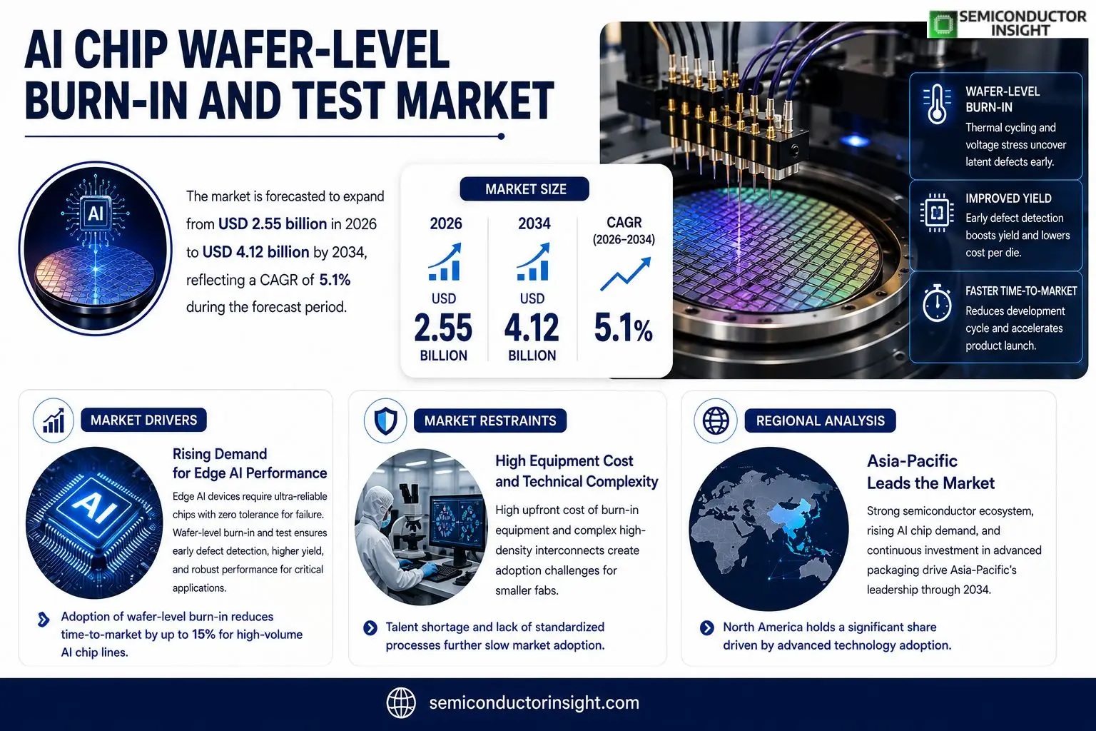
AI Chip Wafer-Level Burn-In and Test market size was valued at USD 2.48 billion in 2025. The market is forecasted to expand from USD 2.55 billion in 2026 to USD 4.12 billion by 2034, reflecting a CAGR of 5.1 % during the forecast period.
Wafer‑level burn‑in and test refers to the systematic stress‑testing of AI semiconductor wafers before dicing, using temperature cycling, voltage stressing, and functional verification directly on the wafer surface. This approach uncovers latent defects early, improves yield, and shortens time‑to‑market for high‑performance AI processors that operate at extreme frequencies.The upward trajectory stems from exploding demand for edge‑AI accelerators and data‑center GPUs, which require stringent reliability guarantees because downtime translates into substantial revenue loss. At the same time, rising capital expenditure on advanced packaging encourages manufacturers such as ASE Technology Holding, TSMC, and Foundries to integrate wafer‑level testing into their production lines. However, the steep upfront cost of specialized burn‑in equipment tempers adoption speed among smaller fabs.
MARKET DRIVERS
Rising Demand for Edge AI Performance
Manufacturers of autonomous vehicles, smart cameras, and robotics are demanding chips that can process data at the edge with minimal latency. Wafer‑level burn‑in and test provides the reliability needed to meet those performance thresholds, prompting OEMs to tighten qualification cycles. The shift away from cloud‑centric models amplifies the necessity for robust on‑chip validation early in production.
Cost Pressures Favor Integrated Test Solutions
Traditional probe‑based testing imposes high handling costs and introduces yield‑loss risk. By embedding burn‑in and test steps at the wafer stage, fabs can consolidate equipment footprints and lower per‑die expense. Cost efficiencies realized through this integration are compelling for both legacy semiconductor players and emerging AI‑chip startups.
➤ Adoption of wafer‑level burn‑in reduces time‑to‑market by up to 15 % for high‑volume AI chip lines, delivering a measurable competitive edge.
Regulatory scrutiny over safety‑critical AI applications is tightening. Certification bodies increasingly require documented stress‑testing data before granting approval. The compliance advantage offered by wafer‑level procedures aligns with this evolving oversight, further stimulating market uptake.
MARKET CHALLENGES
Technical Complexity of High‑Density Interconnects
Modern AI chips feature dense micro‑bump arrays and heterogeneous integration, complicating uniform thermal cycling during burn‑in. Engineering reliable test patterns that avoid false failures demands sophisticated simulation tools, raising the entry barrier for smaller fabs.
Other Challenges
Equipment Capital Intensity
Acquiring wafer‑level burn‑in platforms entails multi‑million‑dollar investments. Companies with limited capex flexibility may defer adoption, opting for outsourced solutions that add lead time.
Process Standardization Gaps
Industry‑wide standards for burn‑in parameters are still maturing. Divergent practices across regions can cause inconsistencies in yield reporting, hampering cross‑border collaborations.
MARKET RESTRAINTS
Limited Availability of Skilled Personnel
The specialized knowledge required to design, operate, and interpret wafer‑level burn‑in data is scarce. Training cycles extend beyond the typical product development timeline, and the shortage of qualified engineers can slow implementation rates.
Thermal Budget Constraints for Advanced Nodes
As AI chips transition to sub‑3 nm processes, the allowable temperature exposure shrinks dramatically. Balancing sufficient stress to uncover latent defects without exceeding thermal budgets creates a narrow operational window, limiting the applicability of conventional burn‑in profiles.
MARKET OPPORTUNITIES
AI Chip Wafer-Level Burn-In and Test Market
Emerging AI accelerator architectures that integrate photonic and neuromorphic elements present a fresh frontier for wafer‑level validation. Early adopters who tailor burn‑in cycles to these novel materials can differentiate their solutions and capture premium market share.Strategic partnerships between equipment manufacturers and AI‑chip designers are forming to co‑develop programmable burn‑in modules. Such collaborations promise faster cycle times and enable real‑time defect analytics, opening avenues for subscription‑based testing services.Geographically, regions investing in sovereign AI semiconductor capabilitiesparticularly in Southeast Asiaare earmarking public funds for advanced testing infrastructure. This fiscal support creates a fertile environment for vendors to expand footprint and secure long‑term contracts.
AI Chip Wafer-Level Burn-In and Test Market Trends
Rising Reliability Demands for Edge and Data‑Center AI Processors
The proliferation of AI workloads at the edge and within hyperscale data centers has amplified the tolerance for failure to near‑zero levels. Customers now require processors that can sustain extreme frequency spikes without intermittent faults, because a single outage can jeopardize mission‑critical services and erode brand credibility. Wafer‑level burn‑in and test offers a pre‑emptive safeguard, exposing latent defects before the dice stage and thereby preserving yield while shortening the validation cycle. This capability aligns tightly with the strategic objectives of OEMs seeking to differentiate on uptime, prompting a noticeable shift toward incorporating wafer‑level reliability checks as a standard step in the production flow of AI chips.
Other Trends
Capital Investment in Advanced Packaging Fuels Test Integration
Advanced packaging techniques such as chip‑on‑wafer and heterogeneous integration demand tighter process control, which in turn raises the stakes for early‑stage defect detection. Leading foundriesincluding ASE Technology Holding, TSMC, and Foundriesare allocating budget toward dedicated burn‑in chambers that can operate under the thermal‑mechanical profiles required by 3D‑stacked AI modules. By embedding wafer‑level testing directly into the packaging line, these fabs reduce hand‑off delays and improve overall throughput. The move reflects a broader industry calculus: the incremental spend on testing equipment is offset by higher first‑pass yields and a smoother ramp‑up of new AI processor families.
Equipment Cost Barriers and Consolidation of Testing Services
Despite the clear upside, the initial capital outlay for specialized burn‑in rigs remains a deterrent for smaller fabs and emerging design houses. High‑temperature cycling units and precision voltage‑stress apparatus carry price tags that can strain modest capex plans, leading many to outsource the wafer‑level test function to third‑party service providers. This outsourcing trend is encouraging the emergence of niche testing firms that operate at scale, offering shared‑use facilities that spread cost across multiple clients. For the broader AI Chip Wafer-Level Burn-In and Test Market, the implication is a gradual consolidation of testing services, where a handful of capable players become pivotal enablers for the ecosystem while smaller manufacturers focus on design innovation.
COMPETITIVE LANDSCAPE
Key Industry Players
AI Chip Wafer‑Level Burn‑In and Test Market – Competitive Overview
The segment is dominated by a handful of integrated circuit foundries that have woven wafer‑level burn‑in into their standard process flow. ASE Technology Holding, TSMC and Foundries each run dedicated burn‑in lines that couple thermal cycling with voltage stress, enabling them to catch latent defects before dicing. Their scale permits amortisation of the high capital outlay, while close ties to AI‑chip designers give them visibility into reliability specifications that matter for edge accelerators and data‑center GPUs. This concentration creates a two‑tier structure: a core of vertically‑integrated fabs that control both silicon and test, and a peripheral of specialised equipment suppliers that support the core’s testing needs. The arrangement encourages rapid feedback loops, improves first‑pass yield and shortens the time required to bring AI processors to market, a decisive advantage as customers demand ever‑higher clock rates.Beyond the primary fabs, a constellation of niche players contributes essential capabilities. Applied Materials and Qorvo supply boutique burn‑in chambers and RF‑level stress modules that address niche frequency bands and power‑density envelopes. Intel and NVIDIA have opened dedicated test bays to validate their own AI silicon, while Samsung Electronics leverages its advanced packaging portfolio to embed wafer‑level verification into 3D‑stacked devices. European firms such as STMicroelectronics, Infineon Technologies and NXP Semiconductors offer modular test solutions that appeal to smaller fab operators facing steep equipment costs. The breadth of these contributors widens the competitive field, drives incremental innovation in stress‑profile algorithms, and creates opportunities for partnerships that can lower entry barriers for emerging AI‑chip makers.
List of Key AI Chip Wafer-Level Burn-In and Test Companies Profiled
- ASE Technology Holding
- TSMC
- Foundries
- Applied Materials
- Intel
- NVIDIA
- Samsung Electronics
- Qorvo
- STMicroelectronics
- Infineon Technologies
- NXP Semiconductors
- Renesas Electronics
- Analog Devices
- Micron Technology
- Texas Instruments
Segment Analysis:
| Segment Category | Sub-Segments | Key Insights |
| By Type |
|
Mixed-signal AI processors
|
| By Application |
|
Edge AI devices
|
| By End User |
|
Semiconductor fabs
|
| By Technology |
|
Thermal stress burn‑in
|
| By Test Methodology |
|
Automated wafer probing
|
Regional Analysis: AI Chip Wafer-Level Burn-In and Test Market
North America
Leading fabs have integrated AI‑enhanced diagnostic kernels into the burn‑in stage, allowing real‑time pattern recognition of emerging failure modes. This capability shortens the feedback loop between wafer production and design iteration, reinforcing the region’s reputation for rapid technology turnover.
Recent disruptions highlighted the importance of dual‑sourcing critical test equipment. North American firms have responded by establishing localized component inventories and forging strategic alliances with domestic equipment makers, mitigating exposure to overseas logistics volatility.
Federal initiatives incentivize on‑site testing to reduce waste and improve energy efficiency. Grant programs specifically target upgrades to wafer‑level burn‑in platforms, accelerating the migration toward greener manufacturing practices.
Cloud service providers and autonomous‑vehicle developers are pushing for tighter defect tolerances. Their procurement criteria now explicitly require documented wafer‑level validation, influencing fab scheduling priorities and driving higher utilization of burn‑in capacity.
Europe
European players are leveraging the region’s strong standards framework to differentiate their AI Chip Wafer-Level Burn-In and Test Market offerings. The emphasis on interoperability across EU‑wide research consortia encourages the sharing of test data sets, which in turn supports more robust predictive models. While capacity lags behind North America, targeted public‑private partnerships are channeling funds into next‑generation test equipment, aiming to close the gap. OEMs in Europe are also prioritizing sustainability, prompting vendors to embed energy‑monitoring features into burn‑in stations, a move that aligns with broader EU environmental directives.
Asia‑Pacific
Asia‑Pacific’s rapid expansion of fab real estate translates into a growing appetite for wafer‑level verification. Countries such as Taiwan and South Korea have begun to embed AI‑driven burn‑in modules directly into line‑side tooling, a practice that shortens cycle time for high‑volume AI chips. However, the region’s fragmented supply base sometimes hampers uniform adoption of best‑in‑class test protocols. Collaborative initiatives led by regional chip alliances are attempting to standardize methodologies, which could unlock efficiencies for both domestic and export‑oriented manufacturers.
South America
South American semiconductor activities remain nascent, yet the region is cultivating a niche in low‑cost, high‑volume AI chip production. Emerging foundries are adopting wafer‑level burn‑in as a cost‑effective means to achieve acceptable yields without extensive post‑fab rework. Government incentives aimed at building a local semiconductor ecosystem have spurred investment in modest‑scale test equipment, positioning the market to capture growing demand from regional automotive and IoT sectors.
Middle East & Africa
In the Middle East & Africa, AI Chip Wafer-Level Burn-In and Test Market is largely driven by government‑sponsored technology parks that seek to attract foreign fab operators. Early‑stage projects focus on integrating smart‑test solutions that can be monitored remotely, a feature that appeals to operators dealing with limited on‑site expertise. Although overall volume is limited, the region’s strategic location offers a logistical advantage for serving both European and Asian customers, encouraging a gradual buildup of specialized testing capabilities.
Report Scope
This market research report provides a comprehensive analysis of the AI Chip Wafer-Level Burn-In and Test Market , covering the forecast period 2026–2034. It offers detailed insights into market dynamics, technological advancements, competitive landscape, and key trends shaping the industry.
Key focus areas of the report include:
- Market Overview: The report begins with an overview outlining its current market scenario, key growth indicators, and industry transformation drivers. It discusses macroeconomic factors, demand–supply balance, regulatory landscape, and the strategic role of semiconductors in powering advancements across industries such as automotive, telecommunications, consumer electronics, and industrial automation.
- Market Size & Forecast: Historical data and future projections for revenue, unit shipments, and market value across major regions and segments.
- Segmentation Analysis: Detailed breakdown by product type, technology, application, and end-user industry to identify high-growth segments and investment opportunities.
- Regional Insights: Insights into market performance across North America, Europe, Asia-Pacific, Latin America, and the Middle East & Africa, including country-level analysis where relevant.
- Competitive Landscape: Profiles of leading market participants, including their product offerings, R&D focus, manufacturing capacity, pricing strategies, and recent developments such as mergers, acquisitions, and partnerships.
- Technology Trends & Innovation: Assessment of emerging technologies, integration of AI/IoT, semiconductor design trends, fabrication techniques, and evolving industry standards.
- Market Drivers & Restraints: Evaluation of factors driving market growth along with challenges, supply chain constraints, regulatory issues, and market-entry barriers.
- Stakeholder Insights: Insights for component suppliers, OEMs, system integrators, investors, and policymakers regarding the evolving ecosystem and strategic opportunities.
Primary and secondary research methods are employed, including interviews with industry experts, data from verified sources, and real-time market intelligence to ensure the accuracy and reliability of the insights presented.
FREQUENTLY ASKED QUESTIONS:
What is the current market size of AI Chip Wafer-Level Burn-In and Test Market?
-> AI Chip Wafer-Level Burn-In and Test Market was valued at USD 2.48 billion in 2025 and is expected to reach USD 4.12 billion by 2034.
Which key companies operate in AI Chip Wafer-Level Burn-In and Test Market?
-> Key players include Axalta Coating Systems, AkzoNobel, BASF SE, PPG, Sherwin-Williams, and 3M, among others.
What are the key growth drivers?
-> Key growth drivers include railway infrastructure investments, urbanization, and demand for durable coatings.
Which region dominates the market?
-> Asia-Pacific is the fastest-growing region, while Europe remains a dominant market.
What are the emerging trends?
-> Emerging trends include bio-based coatings, smart coatings, and sustainable rail solutions.
Get Sample Report PDF for Exclusive Insights
Report Sample Includes
- Table of Contents
- List of Tables & Figures
- Charts, Research Methodology, and more...
 Download Sample Report PDF



