
AI Chip Process Monitor IP Market Insights
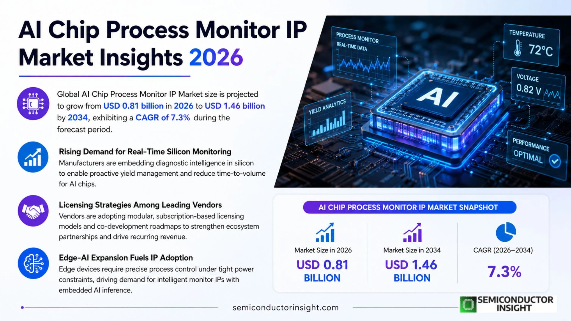
Global AI Chip Process Monitor IP Market size was valued at USD 0.78 billion in 2025. The market is projected to grow from USD 0.81 billion in 2026 to USD 1.46 billion by 2034, exhibiting a CAGR of 7.3% during the forecast period.
AI Chip Process Monitor IP comprises intellectual property cores that enable real‑time monitoring of semiconductor manufacturing steps such as lithography exposure, etch depth control, and thermal profiling within AI accelerator chips. These cores integrate sensor data fusion, on‑chip analytics, and feedback loops to maintain yield and performance while reducing defect rates.
The market is gaining momentum because AI workloads are pushing chip complexity, prompting manufacturers to adopt advanced monitoring solutions that safeguard silicon reliability. Moreover, heightened capital spending on AI data‑center infrastructure and emerging edge‑AI deployments are encouraging foundries to license sophisticated monitor IPs. Companies like Arm Ltd., Synopsys Inc., Cadence Design Systems, and Imec are actively expanding their portfolios through strategic collaborations and technology refreshes.
MARKET DRIVERS
Rising Demand for Edge AI Inference
Enterprises are deploying AI models at the edge to reduce latency and protect data sovereignty. This shift forces silicon vendors to embed sophisticated process‑monitoring IP directly into AI chips, ensuring that performance targets are met without resorting to costly post‑silicon debugging. The necessity to maintain consistent power‑efficiency ratios while scaling compute density makes advanced monitoring indispensable, and firms that provide integrated IP are gaining preferential treatment in design contracts.
Increasing Complexity of Chip Design Verification
Modern AI accelerators incorporate heterogeneous cores, high‑bandwidth memory stacks, and specialized interconnects. Verifying this ecosystem within acceptable timeframes requires continuous in‑silicon visibility. Vendors that supply real‑time process‑monitor IP enable design teams to detect thermal hotspots, voltage irregularities, and timing violations early, thereby trimming development cycles and preserving margins. The competitive edge comes from converting these insights into automatic runtime adjustments.
➤ Integration of real‑time monitoring accelerates time‑to‑market while safeguarding yield targets.
Collectively, these forces encourage semiconductor companies to embed AI Chip Process Monitor IP as a standard design block. Strategic adoption not only curtails rework costs but also builds credibility with OEMs seeking predictable performance across diverse operating environments.
MARKET CHALLENGES
IP Licensing Cost Pressures
Licensing fees for high‑fidelity monitoring IP have risen in tandem with feature richness. Start‑ups and midsize fabless firms often confront budget constraints that force them to prioritize core compute IP over auxiliary monitoring blocks. This trade‑off can expose projects to latent reliability risks, especially when design timelines are compressed.
Other Challenges
Supply Chain Volatility
Component shortages and logistics bottlenecks complicate the acquisition of compatible test equipment needed to validate process‑monitor solutions. Without a stable supply chain, the rollout of new IP versions may stall, delaying product introductions and eroding confidence among design partners.
MARKET RESTRAINTS
Standardization Gaps
Industry‑wide standards for AI chip monitoring interfaces remain fragmented. Design teams must navigate multiple proprietary APIs, which inflates integration effort and raises the risk of incompatibility across successive silicon generations. Until a consensus emerges, the market will see uneven adoption rates and slower diffusion of advanced monitoring capabilities.
MARKET OPPORTUNITIES
Emerging Applications in Autonomous Systems
Autonomous vehicles, drones, and robotics demand continuous health‑checking of AI processors to guarantee safe operation under variable environmental conditions. Embedding AI Chip Process Monitor IP offers real‑time diagnostics that can trigger fail‑safe mechanisms, creating a compelling value proposition for OEMs seeking regulatory compliance and brand trust. Companies that tailor their IP for these safety‑critical scenarios stand to capture a rapidly expanding revenue stream.
AI Chip Process Monitor IP Market Trends
Rising Demand for Real‑Time Silicon Monitoring
The acceleration of AI workloads is compelling semiconductor manufacturers to embed diagnostic intelligence directly into silicon. By continuously sampling lithography exposure, etch depth and thermal conditions, monitor IPs create a closed‑loop that corrects variations before they translate into yield loss. This shift from post‑fab inspection to proactive, on‑chip governance reduces defect propagation and shortens time‑to‑volume for new AI accelerators, a benefit that resonates across data‑center and edge deployments.
Other Trends
Licensing Strategies Among Leading Vendors
Suppliers such as Arm Ltd., Synopsys Inc., Cadence Design Systems and Imec are moving beyond one‑off licensing toward modular, subscription‑based models. These arrangements allow foundries to scale monitor capabilities in step with design complexity, while preserving cash flow flexibility. Collaborative road‑maps between IP owners and silicon players also surface, whereby co‑development clauses lock in early‑access to next‑generation analytics blocks, reinforcing ecosystem lock‑in and driving incremental revenue streams.
Edge‑AI Expansion Fuels IP Adoption
Edge deployments introduce stringent power envelopes and limited cooling budgets, raising the stakes for precise process control. Monitor IPs that fuse sensor inputs with lightweight AI inference enable autonomous adjustment of voltage and frequency, preserving performance under variable thermal loads. As manufacturers target aggressive form‑factor milestones, the ability to guarantee silicon reliability without extensive external test equipment becomes a decisive competitive advantage, prompting a noticeable uptick in licensing activity for edge‑focused monitoring cores.
COMPETITIVE LANDSCAPE
Key Industry Players
Competitive Landscape of AI Chip Process Monitor IP Market
AI Chip Process Monitor IP market is dominated by a handful of large semiconductor IP vendors that leverage extensive design‑automation ecosystems and deep foundry relationships. Arm Ltd. leads the space with its comprehensive suite of safety‑critical and performance‑monitoring IP that is pre‑qualified across major AI accelerator designs, while Synopsys Inc. and Cadence Design Systems provide competing monitor cores integrated into their broader verification and physical‑design platforms. Imec contributes advanced sensor‑fusion IP that is increasingly adopted by European fabless players seeking to improve yield on emerging 3‑nm AI chips. These incumbents benefit from strong licensing revenues, strategic collaborations with foundries such as TSMC and Samsung, and the ability to bundle monitor IP with broader design‑to‑silicon services, creating a market structure that favors integrated, end‑to‑end solutions.
Beyond the dominant tier, a diverse set of niche specialists and emerging innovators enrich the competitive landscape. Companies like SiFive and Rambus focus on open‑source and security‑oriented monitoring blocks that appeal to customized AI edge silicon. GlobalFoundries and Intel’s Custom Foundry division offer proprietary monitor IP tuned for their internal process stacks, while Qualcomm and NXP embed lightweight monitoring cores into AI‑enabled SoCs for mobile and automotive markets. Start‑ups such as Everspin Technologies and Efabless are experimenting with on‑chip magnetic sensor integration and rapid prototyping services, respectively, creating additional pressure on incumbents to accelerate feature updates and price competitiveness.
List of Key AI Chip Process Monitor IP Companies Profiled
- Arm Ltd.
- Synopsys Inc.
- Cadence Design Systems
- Imec
- TSMC
- Samsung Electronics
- Intel Corp.
- GlobalFoundries
- Qualcomm
- NXP Semiconductors
- Texas Instruments
- AMD
- SiFive
- Rambus
- Everspin Technologies
Segment Analysis:
| Segment Category | Sub-Segments | Key Insights |
| By Type |
|
Digital Monitor IP is gaining traction because it aligns closely with the high‑speed data pathways inside AI accelerators.
|
| By Application |
|
Data‑Center AI Accelerators dominate due to the critical need for sustained silicon reliability at scale.
|
| By End User |
|
Chip Foundries prioritize process‑monitor IP to ensure that each wafer meets stringent yield expectations.
|
| By Technology Node |
|
Sub‑10nm Nodes emerge as the focal point because monitoring complexity intensifies as dimensions shrink.
|
| By Development Stage |
|
Mature Deployment dominates the landscape as organizations seek proven IP blocks with established support ecosystems.
|
Regional Analysis: AI Chip Process Monitor IP Market
Universities and research consortia in the region supply a steady flow of patents covering nanoscale temperature sensing and on‑chip error correction. Licensing agreements often bundle these advances with existing IP portfolios, allowing chip designers to adopt monitoring capabilities without incurring extensive development cycles.
Federal agencies encourage transparent manufacturing practices through compliance programs that reference on‑die monitoring. While the regulations are not prescriptive, they create a business environment where robust process‑monitoring IP is viewed as a risk‑mitigation asset.
Major foundries incorporate IP verification steps into their production queues, meaning that customers receive silicon that has already been vetted for process stability. This reduces downstream debugging costs and accelerates time‑to‑market for AI‑focused products.
Enterprises deploying large‑scale AI clusters prioritize chips that can self‑diagnose and report anomalies, preserving service‑level agreements. The promise of lower warranty claims motivates procurement teams to favor designs that embed comprehensive monitoring IP.
Europe
European fabless firms and foundries are increasingly collaborating through cross‑border consortia that share IP roadmaps. The region’s emphasis on energy‑efficient design pushes manufacturers to embed monitoring that can dynamically throttle power consumption without sacrificing AI performance. Local standards bodies are drafting reference guidelines that could streamline interoperability across EU member states, offering a potential edge for vendors that align early with these specifications. Customer sentiment leans toward modular IP solutions that can be swapped as process technologies evolve, a trend that encourages a vibrant secondary market for licensed monitor blocks.
Asia‑Pacific
China, Taiwan, South Korea and Japan form a dense manufacturing corridor where volume drives economies of scale. Governments in these economies subsidize advanced packaging, creating incentive structures for integrating AI‑specific monitoring IP into system‑in‑package solutions. While the region excels at cost‑effective production, it grapples with intellectual‑property enforcement, prompting multinational licensors to adopt hybrid models that blend direct licensing with joint‑development agreements. The rise of edge computing in mobile and automotive sectors fuels demand for compact monitor IP that can operate under constrained power budgets.
South America
Investment in semiconductor infrastructure remains modest, yet Brazil and Mexico are nurturing niche design houses that target specific AI applications such as agritech analytics and renewable‑energy management. These firms view process‑monitoring IP as a differentiator that can assure reliability in harsh environmental conditions. Partnerships with North American licensors supply the technical know‑how, while regional trade agreements facilitate cross‑border technology transfer, gradually expanding the market footprint.
Middle East & Africa
The market in this geography is embryonic, with a handful of startups exploring AI inference at the edge for oil‑field monitoring and telecom infrastructure. Reliance on imported fabs makes process‑monitoring IP essential for meeting stringent uptime requirements. Recent sovereign wealth fund allocations toward tech parks hint at a longer‑term strategy to cultivate local IP creation capabilities, potentially turning the region into a niche supplier of customized monitoring blocks for desert‑grade hardware.
Report Scope
This market research report provides a comprehensive analysis of the AI Chip Process Monitor IP Market , covering the forecast period 2026–2034. It offers detailed insights into market dynamics, technological advancements, competitive landscape, and key trends shaping the industry.
Key focus areas of the report include:
- Market Overview: The report begins with an overview outlining its current market scenario, key growth indicators, and industry transformation drivers. It discusses macroeconomic factors, demand–supply balance, regulatory landscape, and the strategic role of semiconductors in powering advancements across industries such as automotive, telecommunications, consumer electronics, and industrial automation.
- Market Size & Forecast: Historical data and future projections for revenue, unit shipments, and market value across major regions and segments.
- Segmentation Analysis: Detailed breakdown by product type, technology, application, and end-user industry to identify high-growth segments and investment opportunities.
- Regional Insights: Insights into market performance across North America, Europe, Asia-Pacific, Latin America, and the Middle East & Africa, including country-level analysis where relevant.
- Competitive Landscape: Profiles of leading market participants, including their product offerings, R&D focus, manufacturing capacity, pricing strategies, and recent developments such as mergers, acquisitions, and partnerships.
- Technology Trends & Innovation: Assessment of emerging technologies, integration of AI/IoT, semiconductor design trends, fabrication techniques, and evolving industry standards.
- Market Drivers & Restraints: Evaluation of factors driving market growth along with challenges, supply chain constraints, regulatory issues, and market-entry barriers.
- Stakeholder Insights: Insights for component suppliers, OEMs, system integrators, investors, and policymakers regarding the evolving ecosystem and strategic opportunities.
Primary and secondary research methods are employed, including interviews with industry experts, data from verified sources, and real-time market intelligence to ensure the accuracy and reliability of the insights presented.
FREQUENTLY ASKED QUESTIONS:
What is the current market size of AI Chip Process Monitor IP Market?
-> AI Chip Process Monitor IP Market size is projected to grow from USD 0.81 billion in 2026 to USD 1.46 billion by 2034, exhibiting a CAGR of 7.3%
Which key companies operate in AI Chip Process Monitor IP Market?
-> Key players include Arm Ltd., Synopsys Inc., Cadence Design Systems, and Imec, among others.
What are the key growth drivers?
-> Key growth drivers include increasing AI workload complexity driving chip design sophistication, rising capital spending on AI data‑center infrastructure, and expanding edge‑AI deployments.
Which region dominates the market?
-> The provided reference does not specify a dominant region for AI Chip Process Monitor IP Market.
What are the emerging trends?
-> Emerging trends include strategic collaborations among IP vendors, technology refresh cycles, and the integration of advanced sensor fusion with on‑chip analytics.

Get Sample Report PDF for Exclusive Insights
Report Sample Includes
- Table of Contents
- List of Tables & Figures
- Charts, Research Methodology, and more...
 Download Sample Report PDF


